Full-Wave Comparison of Z-cut and X-cut Lithium
Niobate (LiNbO
3
) Electrooptic Modulators Using
Finite Element Method
T. Gorman and S. Haxha
Abstract:In this study we compare the relative merits of Z-cut and X-cut lithium niobate (LN) electrooptic modulators. The finite element method (FEM) has been used to implement a full wave analysis of the two structures and determine the microwave effective index Nm, the characteristic impedance Zc,
the microwave losses αc and the half wave voltage VπL,
operating at frequency range from 0.1 to 100GHz. Modelling of the diffusion profile of the optical waveguides has also been presented. The aim of the comparison of the two devices was to determine which device exhibit lower drive voltage at a high frequency operation.
Index Terms—Electrooptic modulators, communication systems,
drive voltage, conductor loss.
I. INTRODUCTION
Imperative for the communication industry to continue its transition into the next generation of ultra-high-speed communications is the development of low chirp, low drive power and high bandwidth external modulators. Mach-Zehnder (MZ) devices designed from either Z-cut or X-cut LN are the most common external modulators in operation today, operating at frequencies between 10 and 40GHz. Modulators based on Z-cut configuration have often been favoured as it is a relatively simple task to simultaneously match the microwave and optical signals and the characteristic impedance by increasing the buffer layer thickness between electrode and LN substrate. However this comes at the cost of increased drive voltage. Modulators based on the X-cut configuration do not necessarily require a buffer layer since the optical waveguides are placed between the electrodes rather than directly under them. Thus, optical absorption losses are not an issue here. Removal of the buffer layer allows for more of the modulating electric field to penetrate into the waveguide thereby increasing the electrooptic effect and consequently reducing the drive voltage. However the removal of the buffer layer means that velocity and impedance matching is made much more difficult and usually results in narrow electrode gaps and narrow bandwidths. A further advantage of X-cut LiNbO3 modulators is that due to their symmetry the chirp is very low.
Manuscript received March 27, 2007.
The authors are with the Broadband and wireless communication group, Department of Electronics
University of Kent, Canterbury CT2 7 NT, UK Tel: +44 (0) 1273 827257 Fax: +44 (0) 1227 456084 Email: S.Haxha@kent.ac.uk
In this study, the finite element method (FEM) has been chosen as the simulation tool for the modulators since it is a well proven technology in this field and is capable of solving for the eigenvalues of complex topologies with features such as angled waveguides and electrodes and anisotropic structure of materials. A full wave-analysis is undertaken in order to determine the effects of frequency on the modulators microwave effective index, Nm characteristic impedance, Zc conductor loss, αc and half-voltage length-product, VπL which is not possible using the typical quasi-TEM analysis. The full-wave analysis is used to solve for the propagation constant rather than the structures capacitance as is the case with the quasi-TEM approximation.
[image:1.595.340.513.379.664.2]The X-cut and Z-cut electrooptic modulators considered in this study are illustrated in Fig.1 and 2, respectively.
[image:1.595.346.512.534.649.2]Fig. 1. X-Cut LiNbO3 Modulator
Fig. 2. Z-Cut LiNbO3 Modulator
For the purpose of this simulation, the topology of both devices is identical with the exception of the positioning of the waveguides and the orientation of the crystal cut. The buffer layer B is 0.6µm, the electrode gap G is 25µm, the central ‘hot’ electrode width S is 8 µm and the electrode height T is varied between 10 and 29µm.
G Gold Electrodes
Optical Waveguides SiO2 Buffer (B)
LN Substrate
S
Gold Electrodes
T
S G
T
SiO2 Buffer (B)
II. THEORY
A. Microwave Analysis
The FEM is used in order to undertake a full-wave analysis of the two devices, it is capable of dealing with complex structures with anisotropic characteristics such as found with LN. Maxwell’s wave equation when considering the anisotropy of materials becomes:
t H E ∂ ∂ − = ×
∇ µ (1)
t E E H ∂ ∂ + = ×
∇ σ ε (2)
where
⎥ ⎥ ⎥ ⎦ ⎤ ⎢ ⎢ ⎢ ⎣ ⎡ = z y x ε ε ε ε 0 0 0 0 0 0 (3)ε
is the diagonal relative permittivity tensors and E and H are the electric and magnetic fields.In order to determine the microwave effective index Nm it is necessary to solve the above equations for the eigenvalues of the fundamental mode using the FEM. The microwave effective index can be calculated from:
0
k
Nm= β (4)
where
β
is the microwave propagation constant and k0 is the free-space wave number which can be expressed as:λ π 2
0=
k (5)
In order to determine the characteristic impedance of the devices we use the power-current definition:
2
2
I P
Zc= (6)
where P is the modal power and I is the current in the z-direction. The modal power P can be determined by solving the Poynting vector:
P=
∫∫
(E×H∗)⋅iz⋅dxdy2
1
(7)
Where * denotes the complex conjugate and
iz is the unit vector in the z-direction. The integration is carried out over the entire waveguide cross section. The current in the z-direction can be determined by:
dxdy E
I=
∫∫
σ z⋅ (8)Where
σ
is the electrode conductivity which for gold is equal to 4.1×10⁷ S/m and the integration is carried out only over the central ‘hot’ electrode.B. Optical Analysis
In order to determine the half wave voltage length product VπL it is necessary to solve for the fundamental optical mode of the device under the influence of an applied microwave electric field. The value of VπL can then be determined by [1, 2]:
β π
π
∆ = V0
L
V (9)
where
∆
β
= β1 - β0 and β1 and β0 are the propagation constants of the fundamental mode of the Mach-Zehnder arms with and without the applied voltage respectively and V0 is the applied voltage.When considering the push-pull effect of the coplanar waveguide we need to consider the change in the propagation constant with respect to both waveguides, since for both X and Z-cut devices the propagation constant is increased in one arm of the guide whilst it is decreased in the other due to the polarity of the applied microwave electric field and the electrooptic effect of the LN waveguide.
In order to determine the frequency dependent drive voltage as a function of frequency Vπ(f) the following expression is used: 10 / ) ( 10 ) ( )
(f V dc m f
Vπ = π − (10)
where the optical response m(f) is measured in dB optical and the value of Vπ(dc) is determined by the value of Vπ calculated from equation (9).
The optical response is calculated by the following [3]:
[
]
⎥⎦ ⎤ ⎢⎣ ⎡ − − − − + + + + × − − − + + − u u ju S u u ju u j S S u j S S S sin ) exp( sin ) exp( ) 2 exp( ) 2 exp( ) 1 ( 1 2 2 1 2 2 1 (11) Where Z Z Z Z S + − = 1 11 S ZZ +ZZ
− =
2 2
2
(12)
and l j Neff Nm fl c
u π αc
2 1 ) ( 1 − = +
III. RESULTS and DISCUSSIONS
C. Microwave analysis
[image:3.595.334.525.209.366.2]We first consider the microwave characteristics of the two modulators, Z-cut and X-cut. In the microwave region the relative permittivity tensor is as discussed in (3) with the permittivity of the LN substrate being 28 in extraordinary axes and 43 in the two ordinary axes. The permittivity of the silicon dioxide (SiO2) buffer layer is 3.9 and the conductivity of the gold electrodes is 4.1×10⁷ S/m. When calculating the optical response we assume that Z1 = Z2 = 50Ω and that Neff of the unmodulated LN waveguide is 2.142. We also set the electrode interaction length to 1cm. First we have investigated the microwave index Nm and microwave loss as a function of frequency for the two devices with the electrode height T = 29µm:
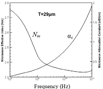
Fig. 3. Variation of microwave effective Index Nm and attenuation constant αc as a function of frequency for Z-cut configuration, when T = 29µm.
[image:3.595.69.264.271.426.2]Clearly both parameters vary significantly with frequency. In particular a significant increase in the attenuation constant can be observed at high frequency operation. The value of Nm decreases rapidly over the first decade up to around 1GHz and then converges to a value of around 2.34 at 100GHz.
Fig. 4. Variation of microwave effective Index Nm and attenuation constant αc as a function of frequency for X-cut configuration, when T = 29µm.
Next we have investigated the same parameters for the X-cut configuration. A similar behaviour of the X-cut is observed and is shown in Fig. 4. This confirms that at a high operating frequency, both the Z-cut and X-cut modulators exhibit similar performance.
[image:3.595.78.259.544.701.2]The frequency dispersion of Nm and αc are almost identical for both Z-cut and X-cut devices, with a slightly lower value of Nm and αc for the X-cut device across the frequency range. Next investigation of the characteristic impedance of the two modulators is carried out.
Fig. 5. Variation of characteristic impedanceas a function of frequency for Z-cut and X-cut configuration, when T = 29µm.
Clearly the X-cut device has a lower Zc at frequencies below 1GHz; however at frequencies above 1GHz the values of Zc are similar, converging to a value of around 39Ω. The characteristic impedance of the two devices is clearly frequency dependent especially at frequencies below 1GHz. This effect can be attributed to the finite value of the electrode conductivity. At low frequencies the increase in Zc can be attributed to the increase in L and R/(ωL)[4] where R and L are the equivalent line resistance and inductance respectively.
By inspection of the graphs above it is clear that neither device is matched to the desired value of Zc=50Ω and the desired value of Nm=2.142 required in order to maximise bandwidth. From previous work [3] it is known that reducing the height of the electrode increases the value of Zc whilst at the same time increasing the value of Nm. It is also known that increasing the buffer layer thickness increases the value of Zc whilst at the same time reducing the value of Nm. The following figures show the effects of reducing the height of the electrodes to 10µm.
T=29µm
Nm
Nm
α
c T=29µmFrequency (Hz) Frequency (Hz)
Frequency (Hz) T=29µm
α
cZ-Cut
Fig. 6.Variation of Nm and αc as a function of frequency for Z-cut configuration when T = 10µm.
[image:4.595.306.554.326.560.2]For the Z-cut configuration, when the electrode height is reduced to 10µm, the value of Nm is increased by around 27% from 2.75 when the electrode height was 29µm, to around 3.5. Again the rate of change in Nm is greatest below around 1GHz. Nm then converges to a value of around 2.8 at 100GHz. The microwave attenuation constant increases by around 3.5dB across the frequency range.
Fig. 7.Variation of Nm and αc as a function of frequency for X-cut configuration when T = 10µm.
For the X-cut device we observe a similar trend, when the electrode height is reduced the value of Nm increases and so does the attenuation constant. Clearly for a low microwave loss device a thicker electrode is desirable though this inevitably results in an increase in Nm.
[image:4.595.83.254.327.474.2]Fig. 8. Variation of characteristic impedanceas a function of
Fig. 8 presents the characteristic impedance Zc for both configurations when T = 10µm.
With respect to both devices the value of Zc has increased significantly, however at higher frequencies the value of Zc is much closer to the desired value of 50Ω.
Clearly in order to produce an optimised device whereby the value of Nm and Zc are simultaneously matched to that of the optical effective index and the impedance of the microwave generator requires that we consider the effects of frequency dispersion on the modulators performance.
D. Optical analysis
Next investigation of the optical properties of the two modulators is carried out. At optical wavelength 1.55µm the refractive index of the LN substrate is around 2.214 with respect to the ordinary optical axes and around 2.138 for the extraordinary. The waveguides are generally formed by titanium indiffusion which increases the refractive index slightly in the waveguide region. The increased refractive index contour is modelled using the following well documented equations [5]:
[
f(x)g(y)]
0.55n n
no= os+∆ o (14)
[
f(x)g(y)]
n n
ne= es+∆ e (15)
Where
⎟ ⎠ ⎞ ⎜ ⎝ ⎛
⎟ ⎠ ⎞ ⎜ ⎝ ⎛ − −
⎟ ⎠ ⎞ ⎜ ⎝ ⎛ + =
dx W erf
dx W x erf dx
W x erf x f
2 2
2 2 2
2 )
( (16)
and
⎥ ⎥ ⎦ ⎤ ⎢
⎢ ⎣ ⎡
⎟⎟ ⎠ ⎞ ⎜⎜ ⎝ ⎛ − =
2
exp ) (
dy y y
g (17)
where nos and nes are the ordinary and extraordinary refractive indexes of LN and ∆no and ∆ne are the maximum ordinary and extraordinary refractive index changes. W is the width of the titanium strip before indiffusion, dx and dy are the diffusion lengths in the x and y directions, respectively. The values for ∆no and ∆ne were taken as 0.0062 and 0.0146 respectively and W=0.6µm. The value of dx = 4.85µm and dy = 4.105µm.
The refractive index of the SiO2 buffer layer was taken as 1.45 and the complex refractive index of the gold electrodes was taken to be 0.379-j10.75. Fig. 9 shows a typical contour plot of the fundamental H11 mode.
T = 10µm T = 10µm
Nm
T=10µm
α
cNm
Frequency (Hz)
Frequency (Hz) Frequency (Hz)
α
cZ-Cut
[image:4.595.74.259.582.738.2]Fig. 9. Contour plot of fundamental H11 mode. Z-cut configuration.
Fig 9 shows that the mode is more tightly confined where the induced change in refractive index is the strongest, evident by the tighter contours nearest to the electrode and less so where the microwave electric field is at its weakest at the extremities of the mode contour. The compressed, spherical shape of the mode is also evidence that the diffusion model is also operating correctly since the highest change in refractive index, caused by the indiffusion process, is directly beneath the centre of the electrode, reducing as the distance increases from this point in the x and y directions.
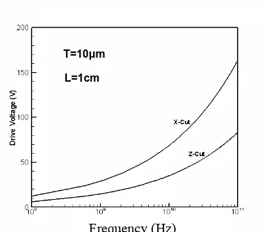
[image:5.595.75.257.53.211.2]In order to calculate the frequency dependence of the drive voltage we determine Vπ(dc) by using (9) then use (10) to determine the frequency response of the drive voltage. The results are presented in Fig. 10 and 11.
Fig. 10. Variation of drive voltage as a function of frequency for Z-cut and X-cut configuration when T = 29µm.
For the Z-cut modulator with T = 29µm the drive voltage is around 9V at the low end of the frequency scale, rising to around 23V at the high end, a significant increase of around 150%. For the X-cut device the drive voltage is significantly higher at around 16V at the low end to around 38V at the higher, an increase of around 138% across the frequency range.
Fig. 11. Variation of drive voltage as a function of frequency for Z-cut and X-cut configuration when T = 10µm.
When the electrode height is reduced to 10µm there is a significant rise in the drive voltage. For the Z-cut device, at the low end of the frequency range, the drive voltage is again around 9V. However, at the upper end of the frequency range it has increased to around 80V, an increase of around 780% over the frequency range. For the X-cut device, again at the low end of the frequency range, the drive voltage is around 12V; however at the high end the drive voltage has increased to around 160V. As can be seen there is a significant increase over the frequency range.
The X-cut device has the higher value of drive voltage and this is no surprise since the electric field strength is reduced firstly by the buffer layer and secondly by the distance that the electrodes are from the active waveguide region (see Fig 1). In order to reduce the drive voltage of the X-cut device total or partial removal of the buffer layer would be required. Or alternatively the electrodes could be positioned closer together to increase the electric field strength around the waveguide. Both of these solutions have issues: firstly by removing the buffer layer the value of Nm is significantly reduced and secondly reducing the electrode gap is known to reduce the bandwidth. A further option is to use thin strip technology whereby a thin strip of LN is bound to a substrate of lower permittivity. Using this technique it is possible to remove the buffer layer completely and at the same time simultaneously match the microwave effective index to the optical effective index and the characteristic impedance of the device to the signal source generator.
T=29µm
L=1cm
T=10µm
L=1cm
Frequency (Hz)
[image:5.595.68.268.440.602.2]IV. CONCLUSION
A full-wave analysis was applied to Z-cut and X-cut electrooptic modulators and the effects of frequency on the microwave effective index, characteristic impedance, attenuation constant and power consumption have been demonstrated. The diffusion profile of the modulator waveguides have also been modelled and presented. It has been demonstrated that the Z-cut device has the lowest value of VπL over the frequency range, however the X-cut devices performance may be significantly improved by the removal of the buffer layer and further investigation (currently underway) into thin film technology in order to improve simultaneous matching of Nm and Zc.
R
EFERENCES[1]. S. Haxha, B. M. A Rahman, R. J. Langley, “Broadband and Low-Driving power LiNbO3 electrooptic modulators”,
Optical and Quantum Electronics, vol. 36, pp. 1205-1220,
2004
[2] B. M. A. Rahman and S.Haxha, “Optimisation of Microwave Properties for Ultrahigh-speed Etched and Unetched Lithium Niobate Electrooptic Modulators”, IEEE,
J. Lightwave Technology, vol. 20, No. 10, pp. 1856-1863,
2002.
[3]. S. Haxha, B. M. A. Rahman, and K.T.V.Grattan, “Bandwidth estimation for ultra-high-speed lithium niobate modulators”, Applied Optics, Vol. 42, No. 15, pp. 2674-2682, 2003.
[4]. W. K Wang, R. W. Smith, P. J Anthony, “Full wave analysis of coplanar waveguides for LiNbO3 optical modulators by the mode matching method considering nonideal conductors on etched buffer layers”, IEEE, J.
Lightwave Technology, vol. 13, pp. 2250-2257, 1995.
[5] E. Strake, G. P. Bava, I. Montrosset,”Guided modes of Ti:LiNbO3 channel waveguides: A novel quasi-analytical technique in comparison with the scalar finite-element method” IEEE, J. Lightwave Technology, vol. 6, pp. 1126-1135, 1998.