Vol. 45, No. 2, Fall 2013, pp. 19- 28 )AIJ-EEE)
٭
Corresponding Author, Email: [email protected]
Capacity Enhancement of Ad Hoc Networks using a New
Beamforming Scheme Based on ESPAR
A. Anbaran
1, A. Mohammadi
2*and A. Abdipour
31- PhD. Student, Microwave/mm-wave and Wireless Communications Research Lab, Amirkabir University of Tehran, Tehran, Iran 2- Professor, Microwave/mm-wave and Wireless Communications Research Lab, Amirkabir University of Tehran, Tehran, Iran
3- Professor Microwave/mm-wave and Wireless Communications Research Lab, Amirkabir University of Tehran, Tehran, Iran
ABSTRACT
This paper proposes a new smart antenna beamforming scheme based on electronically steerable parasitic
array radiator (ESPAR). The proposed method is capable of providing better capacity compared to the
conventional ESPAR. The termination of each antenna element in this structure comprises a PIN diode in
addition to a varactor. Using PIN diode besides the varactor provides more degrees of freedom which lead to
better interference suppression. Moreover, in the proposed method the required tunable impedance range of
the varactors is dramatically reduced. The optimal values of the tunable loads in each simulation scenario
repetition are attained iteratively using steepest descent method with a maximum cross correlation
coefficient criterion. Simulation results show that the proposed scheme outperforms the conventional
ESPAR technique with respect to interference suppression and capacity enhancement. To further validate the
beamforming ability of the proposed method, a testbed was fabricated. Measurement results confirm that the
proposed method can provide an acceptable beamforming capability close to the simulated beam.
KEYWORDS
1-INTRODUCTION
The beamforming systems offer a unique method to enhance the capacity of ad hoc networks [1], [2]. Furthermore, the adaptive beamformers significantly enhance the capacity through interference suppression [3], [4]. Although phased array smart antenna is an efficient technique for maximizing the output signal-to-interference-and-noise power ratio (SINR), this method has limitations in some applications such as ad hoc sensor networks. Using several radio frequency (RF) front-ends and analog-to-digital converters (ADC) increases the manufacturing cost and the power consumption. Moreover, the antenna spacing in phased array systems are in the order of half-wavelength. In [5] we proposed a single-RF beamforming scheme that can achieve an interference suppression capability close to that of a phased array smart antenna while working well at any antenna spacing. However, the complexity of the method proposed in [5] may be unacceptable in some applications.
A reactively controlled dipole antenna in a circular array was introduced in [6] to reduce the size of the circuit and antenna set. Later, this technique was evolved as the electronically steerable parasitic array radiator (ESPAR) [7]-[10]. ESPAR antenna based beamforming provides a very simple architecture for beamforming that has a significantly lower fabrication cost and power [11], which makes it attractive in many applications such as multiple-input multiple-output (MIMO) systems [12], [13], vehicular networks [14], [15] and ad hoc networks [16]. The ESPAR antenna can steer its radiation pattern main lobe toward the desired transmitter and its nulls to the interferer transmitters [17]. Hereby, signal-to-interference ratio (SIR) can be greatly improved, which enhances the capacity in ad hoc networks. However, the ESPAR antenna beamforming performance is far away from the phased array smart antennas performance.
In order to further enhance the performance beyond the ESPAR, a new beamforming scheme is presented in this paper in which beam direction varies by tuning some resistive loads in addition to reactors. PIN diodes are used to realize the resistive tunable loads of each antenna element. Conventional ESPAR systems only use varactors as tunable reactors, although PIN diodes have been used as switches in ESPAR systems [18], [19]. However, to the extent of our knowledge, they have never been used as resistive loads. The proposed configuration enables better control of the radiation pattern.
The values of all tuneable loads are computed iteratively to find the optimal beam. Computer simulations are used to compare the capacity of the conventional ESPAR beamforming system and the new proposed method, in several ad hoc scenarios.
The remainder of this paper is organized as follows: in section 2, the system model is presented and then conventional ESPAR beamforming scheme is introduced. Afterwards, the configuration of the proposed scheme to obtain better performance is described in section 3. In section 4, testbed fabrication and measurement setup are described. Section 5 presents the measurement and simulation results. In section 6, all discussed schemes are
compared from different points of view and finally, a brief conclusion is given in section 7.
2-SYSTEMMODELANDCONVENTIONAL
ESPAR
2-1- SCENARIO MODEL
Consider an ad hoc scenario, where N interferer nodes are located around the desired receiver, interfering with the desired transmitter. The angle of arrival (AOA) of the desired signal is considered at θd degrees. The AOA of the
interferers changes randomly in the range of [+θNI, +180]
and [-180, -θNI] degrees in each iteration, whereas they are
assumed known at the receiver. θNI is defined as the “no
interference angle”, around the desired signal.
An example of such a scenario is shown in Fig. 1. Both systems are supposed to steer their main beam towards the desired signal and null the interferences.
Desired Tx I1
I2
I3
IN θd
No Interference Angle (±θNI)
Fig. 1. An example of the placement of the nodes in our ad hoc scenario
2-2- SYSTEM MODEL
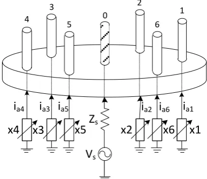
A uniform circular array with center element (UCA-CE) with a radius of R=λ/4 and seven elements is assumed. All of the center and the six surrounding passive elements are considered monopole antennas as shown in Fig. 2.
x3
3 4
5
2
1 6
i
a4i
a3i
a5i
a2i
a6i
a1x5
Z
sx2
x6
x1
0
V
sx4
Fig. 2. A typical ESPAR configuration with six passive elements used as system model
denoting the mutual impedance, zij, between the ith and jth
antenna elements as
66 65 64 63 62 61 60 56 55 54 53 52 51 50 46 45 44 43 42 41 40 36 35 34 33 32 31 30 26 25 24 23 22 21 20 16 15 14 13 12 11 10 06 05 04 03 02 01 00z
z
z
z
z
z
z
z
z
z
z
z
z
z
z
z
z
z
z
z
z
z
z
z
z
z
z
z
z
z
z
z
z
z
z
z
z
z
z
z
z
z
z
z
z
z
z
z
z
Z
a (1)and the symmetry of antenna geometry results in
ji ij
z
z
z
z
z
z
z
z
z
z
z
z
z
z
z
z
z
z
z
z
z
z
z
z
z
z
z
z
z
36 25 14 62 51 46 35 24 13 61 56 45 34 23 12 60 50 40 30 20 10 66 55 44 33 22 11 (2)Therefore, the impedance matrix Za can be described
with only six independent parameters of z00, z10, z11, z12, z13
and z14.
The far-field radiation pattern of this array is the superposition of all antennas‟ radiation patterns [20]. Therefore, the far-field current signal in the azimuthal direction, θ, is represented with its amplitude and phase as
) ( )
(
Ι a
y far T (3)
where I is the current vector of antenna set and a(θ) is the steering vector, which for a UCA-CE can be expressed as T M
R
j
R
j
R
j
a
))
cos(
2
exp(
...
))
cos(
2
exp(
))
cos(
2
exp(
1
)
(
2 1
(4)where R is the radius of the array geometry, λ is the wave length and M is the number of array elements excluding the central one. By substituting R=λ/4 and
M=6, steering vector can be written as
T j j j a )) 3 5 cos( 2 exp( ... )) 3 cos( 2 exp( )) cos( 2 exp( 1 ) ( (5)
Defining the equivalent weight vector, W, as the relation between the antenna current vector, I, and the source voltage, vs, we have
s
Wv
I (6)
Combining (6) and (3), it is clear that the far field radiation pattern of the array can be controlled by the equivalent weight vector.
2-3- CONVENTIONAL ESPAR
The working principle of the conventional ESPAR is described in the literature [17], [21]. The equal weight vector is
1 1
)
(
Z
U
W
a
X
(7)where Za is defined in (1) and U1 is defined as
TU
1
1
0
0
0
0
0
0
(8)and
z jx1 jx2 jx3 jx4 jx5 jx6
diag s
X (9)
where zs and xm are the characteristic impedance of
source and impedance of mth parasitic element, respectively.
3- COMPLEX ESPAR
It can be seen from the former equations that the far field pattern of the conventional ESPAR system is controlled by six independent parameters. We propose a new method to enhance the beamforming ability using twelve independent parameters. In this method, complex impedances are used instead of reactive impedances to load the passive antenna elements. Therefore (9) becomes
6 6 5 5 4 4 3 3 2 2 1 1...
r
jx
r
jx
r
jx
jx
r
jx
r
jx
r
z
diag
s
X
(10)PIN diodes and varactors are used together to realize the complex impedances.
3-1- OPTIMIZATION PROCESS
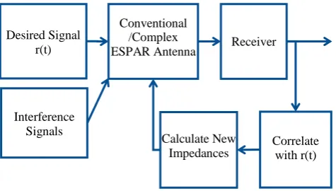
In each simulation run, the received signal at the receiver input is computed as the sum of the desired signal, a known reference signal, and the interference signals, considering their respective angle of arrivals. Next, using the cross-correlation coefficient between the received signal and the reference signal, ρn, the objective
function is computed as the following
2
1
)
(
n nF
X
(11)in which, Xn represents the impedance vector in n-th
repetition.
to ensure that they achieve their best performance in each scenario. At the end of the optimization process, the formed beam of each system is used to compute its output SINR. The process is shown in Fig. 3.
Although we used steepest descent method for optimization and impedance matrix calculation, the proposed scheme is not limited to this optimization method, and all of the other optimization methods proposed for ESPAR systems, such as the one in [21] can be generalized to this scheme.
Fig. 3. Simulation and Optimization Process
3-2- POWER DISSIPATION
As it comes to mind, using lossy components as parasitic elements‟ loads attenuates the signal. The transferred power, P, to the antenna network can be computed by multiplying the antennas‟ voltage vector, V, by the conjugate of the antennas‟ current vector, I, element by element. The voltage of the antennas can be computed by multiplying the antenna impedance matrix by the current vector of antennas. Therefore, a 7-element power vector is formed as
Tp p p p p p p I ZI
P . 0 1 2 3 4 5 6 (12)
Active power is the real part of the power vector. Real part of the p0 represents the total active power that is
drained from the source. Real parts of other elements are negative which represent the dissipated power in complex loads. The dissipated power depends on the tuned impedances. The average total dissipated powers in different scenarios are expressed in Section 5.
4-TESTBED FABRICATION AND
MEASUREMENT SETUP
To achieve as realistic results as possible, a testbed was fabricated and the mutual coupling between elements and some patterns were measured. The target operating frequency of the testbed was 2.4GHz. Antennas were circularly embedded on a circle with a radius of λ/4 in a ground plane.
4-1- TESTBED FABRICATION
Since the varactors cannot realize positive reactances, an inductor should be used to shift the reactance range by half of the total range so that both positive and negative values can be realized in a symmetric range.
In our testbed, Toshiba 1SV287 were used as varactors. Our measurements indicated a capacitance of 1.5pF and 8pF at 10V and -0.5V reverse-bias voltage respectively. Therefore, the varactors implement an impedance range of [-j44, -j8] ohms in our operating frequency. In order to shift the reactance range, a total equivalent inductor of 1.7nH is required to realize an impedance of approximately +j26 ohms. Furthermore, HSMP-3860 from Avago technologies has been used as the PIN diode which can provide a resistance in the range of [3, 1000] ohms.
The series resistance of the varactor diode (approx. 2 ohms), the minimum resistance of the PIN diode (approx. 3 ohms) and the resistance of other elements such as inductor and connector (approx. 1 ohm) should be taken into account. Therefore, a minimum series resistance of 6 ohms should be considered for the proposed method. However, a series resistance of 2 ohms should be considered for the conventional ESPAR system, as well. The dissipated power of both systems is calculated in each scenario which is represented in Section 5.
Since in practice the total electrical length of the SMA connector connected to the antenna is considerable, a transmission line with a length of λ/2 can be used between the antenna and the loads. In order to achieve as realistic results as possible taking into account the electrical length of all used components, the electrical length of the used SMA connector was measured and then the circuit was designed using Agilent Advanced Design System (ADS). The circuit that is used in our fabrication to realize the complex impedances is depicted in Fig. 4. Also the part number of the used components and their manufacturers are summarized in table 1.
D1 Varactor
C1
R1
R2
DC Control 1 Ri
Antenna Element ith
Xi
DC Control 2 D2 PIN Diode
L1 L2
TL1
Fig. 4.The circuit used in our fabricated prototype to realize the complex impedances
TABLE 1. THE PART NUMBERS AND
MANUFACTURERS OF THE COMPONENTS USED IN OUR FABRICATED PROTOTYPE
Parameters Value Manufacturer
RF Substrate RO4003 20mil thickness, ½ oz Rogers Corp.
D1 (Varactor) 1SV287 Toshiba
D2 (PIN diode) HSMP-3860 Avago
Technologies
L1 0302CS-N67XKL (0.67nH) Coilcraft
L2 0302CS-10NXJL (10nH) Coilcraft
R1, R2 1Kohms -
C1 100pF -
In order to simplify the fabrication process, the control components were implemented on a separate PCB and Desired Signal
r(t) Receiver
Interference Signals
Correlate with r(t) Calculate New
Impedances Conventional
connected to the RF board using a few spacers. The control voltages were connected from the control board to the RF board using a pin header connector. The stack up of the fabricated system is depicted in Fig. 5.
Ground Plane Antenna Element ith
SMA Connector
RF Board
Control Board Interface connector
Spacer
Fig. 5. Stack up of the fabricated testbed
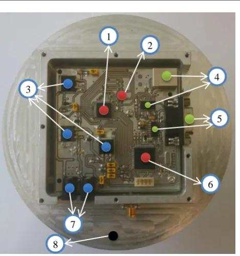
The RF section of the fabricated system is illustrated in Fig. 6. Different parts of the system have been labelled and described. It should be noted that the antennas are connected to the back of the RF board using an SMA connector.
Fig. 6. The RF section of the fabricated prototype
The fabricated control board includes a microcontroller which receives the required control voltages of the varactors from a PC via USB interface. The microcontroller then applies the voltages to the RF board using an Analog Devices AD5360 digital-to-analog converter (DAC). The control board of the fabricated system is depicted in Fig. 7.
Fig. 7. The fabricated control board
4-2- MEASUREMENT SETUP
The mutual coupling and the pattern of the antennas were measured in an anechoic chamber using a reference antenna from Rohde & Schwarz Company. The measurement setup is depicted in Fig. 8.
Fig. 8. The pattern measurement setup
5- EXPERIMENTAL RESULTS
In this section, the results of the carried out experiment in a radio anechoic chamber are discussed.
1
3
4
2
1- Interface between RF & Control Boards (pin Header 2×8) 2- An antenna port
3- 50 Ohm semi-flex RF Cable 4- RF Input Port
3
7
4 1
5 2
6
1- 16 Channel-DAC (AD5360)
2- Interface between RF & Control Boards (pin Header 2×8) 3- Voltage regulators (LM317)
4- USB interface & connector (FT232RL & USB Type B connector) 5- RS232 interface & connector (MAX232 & DB9 connector) 6- Microcontroller (ATMega128)
7- DC Inputs
8- The Antenna Ground Plane
5-1-ANTENNA MUTUAL COUPLING
MEASUREMENTS
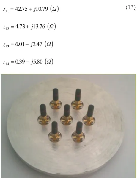
The scattering parameters between each pair of antenna elements were measured using an Agilent vector network analyzer. The impedance matrix, Za, was
computed based on the measurements of scattering parameters. The six independent parameters of Za were as
follows
Ω . j . zΩ . j . z
Ω . j + . z
Ω . j + . z
Ω j + z
Ω . j . z
80 5 39 0
47 3 01 6
76 13 73 4
79 10 75 42
44 . 7 32 . 3
53 9 -90 42
14 13 12 11 10 00
(13)
Fig. 9. The antenna set fabricated to measure the mutual coupling of ESPAR and the proposed scheme
5-2- BEAMFORMING MEASUREMENT
The measurement results of the antenna pattern for a specific scenario are demonstrated in this section. The number of interferer nodes, N, was set to 6 and “no interference angle”, θNI, and the desired signal AOA, θd,
were set to 20 and 30 respectively. The SIR and AOA of each interferer (SIRi and AOAi) were generated randomly.
Then the corresponding impedances were calculated. These parameters are presented in table 2 for the test scenario. Afterwards the formed beam of the proposed method using the calculated impedances was measured in a radio anechoic chamber shown in Fig. 10. For comparison, the simulated normalized beam of the proposed method and the conventional ESPAR system for the test scenario are also shown in Fig. 10. Interferers are
shown by arrows in their respective AOA, such that the SIR is represented by the vertical position of the arrow.
TABLE 2. THE SIR AND AOA OF EACH INTERFERER,
AND THE CORRESPONDING CALCULATED IMPEDANCES OF EACH SYSTEM
Parameters Interferers
1 2 3 4 5 6
Input SIR (dB) 12 13 16 9 7 -14
AOA (Deg) 81 -61 -11 170 -148 135
Vector Elements
1 2 3 4 5 6
Conventional ESPAR Impedances
2.00 +j4.52
2.00 +j1.26
2.00 +j2.99
2.00 -j18.01
2.00 -j14.82
2.00 -j2.14
Proposed Method Impedances
7.53 -j0.10
6.85 -j1.08
7.13 -j0.70
6.09 +j1.12
6.66 -j0.11
6.75 -j0.98
Fig. 10. The measured pattern of the proposed method and the simulated normalized steered beam of both systems, N=6, θNI = 20 degrees and θd = 30 degrees. Interferences and the desired signal are shown by arrows in their respective angle of arrival
As can be seen from Fig. 10, there is a very good agreement between measured and simulated patterns of the proposed method. The small difference between the measurement results and simulation results can be due to the following reasons:
The lack of perfect symmetry in the impedance matrix of the antennas
The tolerance in the values of the components, including the varactors and inductors
As illustrated in Fig. 10, the beamforming performance of the proposed system is considerably superior to that of the conventional ESPAR system. This
-180 -120 -60 0 60 120 180
-50 -40 -30 -20 -10 0 10 20
Desired
Azimuth Plane (Degree)
N
o
rm
a
li
z
e
d
B
e
a
m
(d
B
)
leads to capacity enhancement as well. The effects of this enhancement are described in the next section.
5-3- SIMULATION RESULTS
Conventional ESPAR and the proposed method were simulated to investigate their abilities of beamforming in different ad hoc scenarios. Different numbers of interferers, N, desired angle of arrivals, θd, and “no
interference angles”, θNI, were considered in different
scenarios. To smooth the traces, each scenario was simulated 1000 times, whereas interferers‟ AOA and SIR were changed in each simulation run. The SIR of each interferer was randomly generated in the range of [0, +20] dB. The capacity of both systems in simulation run was computed using calculated output SIR and SNR. Then the average capacity was attained.
The antenna mutual coupling matrix used in the simulations was obtained from the measurement results described in section 5.1.
For N=6, θNI =20 degrees and θd =30 degrees, the
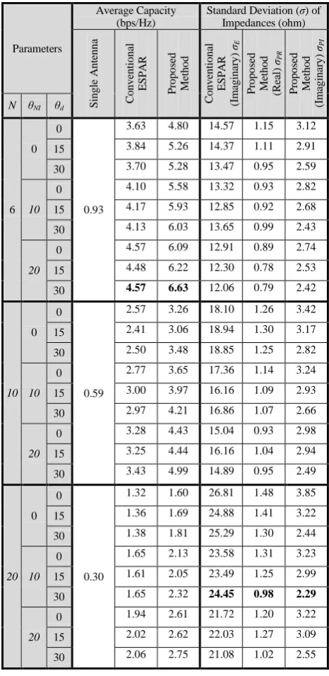
cumulative distribution function (CDF) of the capacity is shown in Fig. 11. It can be observed that for an outage probability of 5%, the capacity of the proposed method was superior compared to the conventional ESPAR system. The outage capacity of the proposed method was 4.3bps/Hz compared to 2.4bps/Hz of the conventional ESPAR system. Furthermore, the average capacity using the proposed method was 6.63bps/Hz compared to 4.57bps/Hz of the conventional ESPAR system.
Fig. 11. Capacity CDF of all systems, N=6, θNI = 20 degrees and θd = 30 degrees. The outage probability of 5% is represented by a line.
To compare the performance of both systems, their average capacities in different scenarios are expressed in table 3. The SNR was assumed to be 30dB which limits the capacity of the systems to 9.96 bps/Hz in each simulation run.
TABLE 3. AVERAGE CAPACITIES IN DIFFERENT
SCENARIOS
Parameters
Average Capacity (bps/Hz)
Standard Deviation (σ) of Impedances (ohm) S in g le A n te n n a C o n v en ti o n al ESP A R P ro p o se d M et h o d C o n v en ti o n al ESP A R (I m ag in ar y ) σE P ro p o se d M et h o d (R ea l) σPR P ro p o se d M et h o d (I m ag in ar y ) σPI
N θNI θd
6 0
0
0.93
3.63 4.80 14.57 1.15 3.12
15 3.84 5.26 14.37 1.11 2.91
30 3.70 5.28 13.47 0.95 2.59
10
0 4.10 5.58 13.32 0.93 2.82
15 4.17 5.93 12.85 0.92 2.68
30 4.13 6.03 13.65 0.99 2.43
20
0 4.57 6.09 12.91 0.89 2.74
15 4.48 6.22 12.30 0.78 2.53
30 4.57 6.63 12.06 0.79 2.42
10
0 0
0.59
2.57 3.26 18.10 1.26 3.42
15 2.41 3.06 18.94 1.30 3.17
30 2.50 3.48 18.85 1.25 2.82
10
0 2.77 3.65 17.36 1.14 3.24
15 3.00 3.97 16.16 1.09 2.93
30 2.97 4.21 16.86 1.07 2.66
20
0 3.28 4.43 15.04 0.93 2.98
15 3.25 4.44 16.16 1.04 2.94
30 3.43 4.99 14.89 0.95 2.49
20
0 0
0.30
1.32 1.60 26.81 1.48 3.85
15 1.36 1.69 24.88 1.41 3.22
30 1.38 1.81 25.29 1.30 2.44
10
0 1.65 2.13 23.58 1.31 3.23
15 1.61 2.05 23.49 1.25 2.99
30 1.65 2.32 24.45 0.98 2.29
20
0 1.94 2.61 21.72 1.20 3.22
15 2.02 2.62 22.03 1.27 3.09
30 2.06 2.75 21.08 1.02 2.55
The span of the required impedances of both systems may be evaluated by the standard deviation of their impedances. This is shown in table 3 as three columns for each scenario. Note that the standard deviation of the real and imaginary parts of the proposed method, represented by σPR and σPI respectively, are calculated separately. It
can be observed from table 3 that the required tunable impedance range of the conventional ESPAR is so much greater than the required tunable impedance range of the proposed method. The average ratio of the standard deviation of the conventional ESPAR impedances, σE, to
standard deviation of real and imaginary parts of the proposed method is calculated in table 4 for different number of interferers.
0 1 2 3 4 5 6 7 8 9
TABLE 4. SUMMARIZED RESULTS OF DIFFERENT
SCENARIOS
Parameters N = 6 N = 10 N = 20
Average Ratio of Standard Deviation of Impedances
σE/σPR 14.15 15.26 19.23 σE/σPI 4.94 5.75 8.11
Average Capacity
@θNI = 20 deg
conventional ESPAR
(bps/Hz) 4.54 3.32 2.01 proposed method
(bps/Hz) 6.31 4.62 2.66 Enhancement 39.0% 39.0% 32.5%
SNR Degradation
(dB)
Conventional ESPAR -1.15 -1.12 -1.06
Proposed Method -2.87 -2.91 -2.93
Difference 1.72 1.79 1.87
The average enhancement of the average capacity in the proposed method compared to the conventional ESPAR is presented in table 4.
Also the SNR degradations of both systems, due to power dissipation of the lossy components, as well as their difference are given in table 4. This shows that the superior performance of the proposed method compared to the conventional ESPAR is achieved by only 1.8 dB antenna gain degradation, which makes the proposed method reasonable in practice.
6- COMPARISON OF ALL SCHEMES
In this section, we compare the discussed schemes from some different points of view.
6-1- MANUFACTURING COMPLEXITY
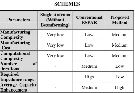
The proposed method requires two variable impedances per antenna element, whereas the conventional ESPAR system requires only one variable impedance per antenna element. Therefore, the proposed method has slightly more manufacturing complexity due to requiring more controllable DC voltages.
6-2- MANUFACTURING COST
The conventional ESPAR system, due to using fewer RF components and controllable DC voltages, has a lower cost compared to the proposed system.
6-3- COMPUTATIONAL COMPLEXITY
Whichever iterative procedure used in both systems, the conventional ESPAR system has a lower computational complexity than the proposed system, due to using fewer controllable DC voltages.
6-4- NUMBER OF ITERATIONS
Since the proposed method has a better ability to steer its nulls, it can achieve the same or better performance than the conventional ESPAR in fewer iterations.
6-5- REQUIRED IMPEDANCE RANGE
The simulation results show that the required tunable range of the impedances in the proposed method is
dramatically reduced. This feature facilitates the diode selection in the proposed system. Furthermore, since the implementable impedance range of the varactors is reduced in higher frequencies, the reduced required impedance range of the proposed method makes it more feasible in higher frequencies compared to conventional ESPAR.
6-6- ANGLE OF ARRIVAL OF THE DESIRED
SIGNAL
Since the angle between each consecutive antenna element pair is 60 degrees, the AOA of the desired signal is considered at three different values at 0, 15 and 30 degrees to evaluate the performance of both systems. The simulation results show that the capacity enhancement in the proposed method is considerable in all cases.
6-7- POWER DISSIPATION
As mentioned before, complex ESPAR will enhance capacity by SIR improvement but its major disadvantage is its lossy nature due to using lossy elements in loads (PIN diodes). This loss can be considered as decreasing antenna gain that leads to degrading SNR directly. The simulation results show that the average loss in antenna gain in the proposed method is about 2.9 dB which is only about 1.8 dB more than that of conventional ESPAR.
As can be seen from table 3, although this SNR degradation does have a small effect on the average capacity at very high capacities, but the performance improvement is still considerable compared to the conventional ESPAR. Furthermore, the output SIR is typically much lower than the SNR; therefore the capacity is limited by the SIR rather than the SNR. This is the case for most ad hoc scenarios.
6-8- AVERAGE CAPACITY
The simulation results show that the average capacity of the proposed method was superior compared to the conventional ESPAR system in different scenarios.
Specifications of both systems are briefly compared in table 5. The single antenna system with no beamforming mechanism is also included for comparison.
TABLE 5. GENERAL COMPARISON OF ALL
SCHEMES
Parameters
Single Antenna (Without Beamforming)
Conventional ESPAR
Proposed Method
Manufacturing
Complexity Very low Low Medium Manufacturing
Cost Very low Low Medium
Computational
Complexity Very low Low Medium Number of
iterations - Medium Low
Required
Impedance range - High Low
Average Capacity
7- CONCLUSIONS
This paper presented a new complex ESPAR method as a beam former smart antenna whose beam direction changes using variable loads (varactors and PIN diodes). Computer simulation results confirmed that the proposed scheme gives significant enhancement in the capacity compared to the conventional ESPAR system (up to 6.6 bps/Hz compared to 4.6 bps/Hz), due to better interference suppression, although it has slightly less antenna gain that degrades the SNR by about 1.8 dB more than the conventional ESPAR. A testbed was fabricated and pattern measurements were carried out to validate the simulation results and a good agreement was observed.
The proposed method can be used in various ad hoc applications such as sensor networks which are typically power- and size-critical. In power-critical systems, the transmitter power can be reduced while keeping the same capacity as conventional systems.
REFERENCES
[1] Seong-Gu Lee; Bum-sik Park; Deok-Hwan Lee; Dong-Hun Lee; Hak-Lim Ko; JeongGil Ko, „Performance analysis of beamforming techniques in ad-hoc communication between moving vehicles,‟ Communications, 2007. APCC 2007. Asia-Pacific Conference on , vol., no., pp.185,188, 18-20 Oct. 2007.
[2] Ananthi, G.; Annie, S.S.; Thiruvengadam, S.J., „Performance analysis of MIMO ad-hoc networks with quantized beamforming and imperfect channel state information,‟ Signal Processing and Communications (SPCOM), 2010 International Conference on , vol., no., pp.1,5, 18-21 July 2010.
[3] H. Kaibin, J.G. Andrews, G. Dongning, R.W. Heath, et al, „Spatial Interference Cancellation for Multiantenna Mobile Ad Hoc Networks‟, IEEE Trans. on Information Theory, Vol. 58 , No. 3, 2012.
[4] C. Dau-Chyrh, H. Cheng-Nan, „Smart Antennas for Advanced Communication Systems‟, Proc. of the IEEE. Vol. 100, No. 7, 2012.
[5] A. Anbaran, A. Mohammadi, A. Abdipour, „Capacity Enhancement of Ad Hoc Networks using a New Single-RF Compact Beamforming Scheme‟, IEEE Trans. on Antennas & Propagation, to be published
[6] R. F. Harrington, „Reactively controlled directive arrays,‟ IEEE Trans. Antennas Propagat., Vol. AP-26, pp. 390–395, May 1978.
[7] Liu Hai-Tao, S. Gao, Loh Tian-Hong, „Electrically Small and Low Cost Smart
Antenna for Wireless Communication‟, IEEE Transactions on Antennas and Propagation, Vol. 60, No. 3, 2012.
[8] O.N. Alrabadi, C.B. Papadias, A. Kalis, N. Marchetti, et al, „MIMO transmission and reception techniques using three-element ESPAR antennas‟, IEEE Communications Letters, Vol. 13, No. 4, 2009.
[9] S.A. Mitilineos, K.S. Mougiakos, Thomopoulos, C.A. Stelios, „Design and Optimization of ESPAR Antennas via Impedance Measurements and a Genetic Algorithm‟, IEEE Antennas and Propagation Magazine, Vol. 51, No. 2, 2009.
[10] H. Liu, S. Gao. ; T. Hong Loh „Compact MIMO Antenna With Frequency Reconfigurability and Adaptive Radiation Patterns‟, IEEE Antennas and Wireless Propagation Letters, Vol. 12, 2013.
[11] K. Gyoda and T. Ohira, „Design of Electronically Steerable Passive Array Radiator (ESPAR) Antennas‟, IEEE Antennas and Propagation Society International Symposium, Vol. 2, pp. 922-925, July 2000.
[12] A. Mohammadi, F.M. Ghannouchi, „RF Transceiver Design for MIMO Wireless Communications‟, Springer publisher, Berlin, 2012.
[13] A. Kalis, A. Kanatas, C. Papadias, „Parasitic Antenna Arrays for Wireless MIMO Systems‟, ISBN 978-1-4614-7998-7, Springer, 2014
[14] A. Anbaran, A. Mohammadi, A. Abdipour, „Capacity Enhancement in Vehicle to Roadside Networks Using ESPAR Technique‟, IEEE International Wireless Symposium (IWS), 14-18 April 2013.
[15] Y. Toor, P. Muhlethaler, A. Laouiti, and A. de La Fortelle, „Vehicle ad hoc networks: Applications and related technical issues,‟ IEEE Communications Surveys & Tutorials, vol. 10, no. 3, pp. 74–88, third quarter 2008.
[16] S. Bandyopadhyay, S. Roy, T. Ueda, „Enhancing the Performance of Ad Hoc Wireless Networks with Smart Antennas,‟ ISBN 978-0-8493-5081-8, Auerbach Publications. 2006.
3033-3039, Nov. 2003.
[18] H. Liu, T. H. Loh and S. Gao, "Compact Low-Cost Smart Antenna for Wireless Communications", 3th European Wireless Technology (EuWiT) Conference (as part of the European Microwave Week), Paris, France, 26th Sept. – 1st Oct. 2010.
[19] H. Liu, S. Gao, and T. H. Loh, "Small Smart Antenna Composed of Reconfigurable Inverted F-type Antenna", 2009 International Conference on Microwave Technology & Computational Electromagnetics (ICMTCE), Beijing, China, 3rd – 6th Nov. 2009.
[20] C. A. Balanis, „Antenna Theory: Analysis and Design‟, 2nd ed. New York: Wiley, 1997, pp. 127–257.