Circuit Architecture for Photon Counting Pixel
Detector with Thresholds Correction
Suliman Abdalla
1, Marwa Mekki
2, and Amin Babiker
3 1Atomic Energy Commission, P.O. Box 3001, Khartoum, Sudan
2Faculty of Engineering, University of Gazira, Wad Medani, Sudan
3Faculty of Engineering, Alneelain University, Khartoum, Sudan
Email: {suliman2003, Marwa_mekki, amin.31766}@hotmail.com
Abstract—In the hybrid pixel detectors, the detector and the readout circuit are constructed separately and then connected electrically by flip-chip bonding. This concept allows the same readout chip to operate using different sensor materials. In photon counting readout, by taking into account the noise around the signal, and other effects such as the variation of amplifier gain and the signal offset. To have a good efficiency for the signals charge, the comparator threshold setting is needed to be low enough. In this paper, a photon counting pixel detector readout with threshold correction is implemented as a solution for the missing counting of the signal due to the offset problem. The additional circuits needed for this architecture, leads to an increase in power consumption and only a marginal increase in circuit area. It is implemented in a 120nm CMOS process and the presented results are based on simulations.
Index Terms—threshold, photon, correction, pixel, noise, discriminator
I. INTRODUCTION
Readout circuits for photon counting image sensors are based on analog and digital circuits, such as the Medipix 2 [1]. Photon-counting pixels contain complex circuitry, which means that the pixel design is mainly driven by area, power consumption and mixed mode design constraints. In photon counting pixel readout of X-rays if a pixel does not have excellent X-ray sensitivity, a low energy threshold and a low noise contribution, then attempts to correct intensity measurements may fail because small changes in threshold can lead to significant alteration in detection efficiency. Because small variations in threshold make it very difficult to avoid missing counts. To solve this problem four discriminators per pixel instead of double discriminators are used. For low discriminator level, the circuit consists of sum circuit and two comparators, one of the comparator work as a threshold correction. For high discriminator level, the circuit consists of two comparators and (AND gate). For improving threshold uniformity, the circuit is equipped with two 5-bits analog to digital converters DACs. One of the DAC is used to bias the feedback transistors of the preamplifier and the shaper. The second DAC set the
Manuscript received August 7, 2014; revised February 11, 2015.
threshold voltages ThLL, ThLH, ThHL, and ThHH in the
comparators see (Fig. 1).
II. METHODOLOGY
A block diagram of the circuit architecture of Photon counting readout with the threshold correction is shown in Fig. 1. The circuit contains an analog signal processing and digital circuitry. The analog parts consists of a charge sensitive amplifier; a shaping filter, four discriminators and include pile-up rejecters, as the design of this circuit involved a 120nm CMOS process using a power supply voltage of 1.2V. In this case a current mode circuit was used which means that the signals are represented by a current. The current mode circuits could be a better choice as the power supply voltages are lowered, since the signal swing is indirectly limited by a reduction of the available supply voltage range [2]. The digital part consists of (AND gate), Sum circuit, All Digital Window Discriminator (ADWD) and an event counter.
ADWD
E.C Shaper
CSA
ThLH
+
-ThHL ThHH
-+ + +
ThLL LL
LH HH
HL
Sum circuit Detector
&
Figure 1. simplified block diagram of the photon counting pixel readout
A. Charge Sensitive Pre-Amplifier
is nMOS transistor with minimum channel length, in order to minimize series white noise the width of transistor is selected to give minimum noise [4]. The bias input current is fed at the gate of transistor M1 falls within the range of 100nA. Transistor M2 constitutes the cascade. Current is supplied to the M1 node via a cascade current source (M4 and M3), which sets M1 in the region of operation [5]. Transistors M2, M3 and M4 are externally biased. In order to drive a low-impedance load, double source followers, transistors (M5-M8) are used in this design to provide a low-impedance output to drive the following pulse shaper stage. The main noise contribution to the total noise of the preamplifier comes from the M1 input, although the noise contribution from the cascade current source is not negligible due to the low power supply and the limited voltage available to degenerate them [6]. The discharging feedback resistor is formed by the drain-source resistance (Rds) of transistor Mf, which is biased by the current DAC to operate in the saturation in quiescent conditions and it enters in strong inversion when a charge signal is detected [7].
The frequency behavior of the CSA is determined by the feedback capacitor Cf and the total parasitic capacitance on the high input impedance node. This capacitance consists of the parallel combination of drain capacitances of transistors M3 and M4, input capacitance and gate capacitance of the subsequent stages.
M4
M3
M7
M8
M2
M1
M5
M6 B3
B2
B1
IN
OUT
B1
RST VDD
Mf
Cf
Figure 2. Circuit diagram for pre-amplifier.
B. Pulse Shaper
The signal detected by the CSA in photon counting readout electronics will generally not be used directly, but will be amplified and shaped. The aim of these procedures is to optimize the signal to noise ratio [8].
The selected pulse shaper must remove low and high frequencies to control signal pile-up and limit the band width. However, while improving the output noise level by limiting the bandwidth, pulse shaping without gain will result in loss of signal and may possibly not provide any real improvement to the output SNR. The amplifier used in the pulse shaper is the same as the one used in the CSA. It is a cascade structure as shown in Fig. 3.
The pulse shaper amplifier has a shaping time of less than 250ns and a bandwidth of 2.4MHz. The simulated noise figure is 42dB less than CSA as expected; the noise
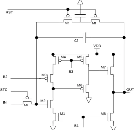
figure is greatly reduced by the pulse shaper. The input transistor M2 receives the signal from CSA via transistor Mi. Current is supplied to the M2 node via a cascade current source (M4 and M9). The second stage of the pulse shaper (not discussed in this paper) consists of a push-pull cascade current source amplifier. In Fig. 3, the output signal OUT of the pulse shaper is fed to a push-pull cascade current source amplifier. In term of power consumption the first stage of pulse shaper uses 246nW in the active mode whereas the second stage increases the power consumption. The shaping time is controlled by the drain-source resistance Rds of the PMOS transistor Mi which is biased by the signal STC that comes from external current mirror. Bias voltages (B1, B2, and B3) come from a bias network, which is common to preamplifier, shaper and comparators. Mf is controlled by the current DAC that allows adjustment of the current simultaneously by the external current.
M5 M4
M6 M9
M2
M1 M8
M7
Mi
Mf Mf
RST
Cf
B2
STC
IN
B1
OUT B3
VDD
Figure 3. Circuit diagram of pulse shaper.
C. Comparator
In photon counting X-ray imaging the signals appear randomly in time and independently in each pixel. After receiving a charge signal from the detector, and having been integrated and shaped, there is a requirement to implement a threshold discriminator in each pixel. In X-ray imaging techniques it is sufficient to measure the spatial distributions of the X-rays of energies above a given threshold (integral discriminator type) or within a given energy window (window discriminator) [9].
M3
M1
M7
M5 M4
M2
M8
M6 M13
M10
M9 M11 M14 M12
Iin Ith
B2
OUT
B1 B3
A
Figure 4. Schematic diagram of comparator.
The comparator is implemented as a cascade current differential amplifier, see Fig. 4. The circuit, made up of the transistors M1-M8, consists of low voltage cascade current mirrors with the output current of the first subtracting from the input of the second. The current in point A equal (Iin - Ith). Where Iin is the input current from pulse shaper and Ith is the threshold current setting by the current DAC. The value of the subtracting current is fed to the push-pull cascade current source, transistors (M9-M14) to generate a voltage output pulse.
D. Sum Circuit
The schematic of the Sum current circuit is based on the current-mode CMOS multiple valued logic circuits [10], is shown in Fig. 5. The circuit received two clock signals from comparators it form lower threshold discriminators LL and LH that drive PMOS switch transistors M6 and M7. The sum of signals is the threshold value. NMOS transistors M4, M5 each provide current to PMOS switches M6 and M7 that are controlled by signal LL and LH respectively. These two low-level currents thresholds are summed at the drain of PMOS transistor M17. This current is fed to the double push-pull cascade current source, transistors (M8-M15) in order to generate a voltage output pulse.
Figure 5. Schematic diagram of sum circuit
Fig. 6 shows a simplified block diagram of the 4 comparators threshold setting. The signals ThLL and ThHL are the threshold setting at the normal state (no
offset), and the signals with dotted lines ThLH and ThHH
are the threshold setting at the offset state.
ThLH
ThLL
ThHL
ThHH
Figure 6. Block diagram of the thresholds setting
E. D/A Converter
In the mode of D/A converter, voltage, current and charge, the current mode conversion in conversion rate has the advantage that voltage swings in the circuit are minimized, which ultimately reduces the sensitivity for parasitic capacitance. In our design, we chose current mode conversion for R-2R ladder D/A converter. The basic structure of digital-to-analog converter is R-2R configuration. Since CMOS switch is not ideal, the resistance of switch affects the accuracy of R-2R network, we adopt CMOS transistors to replace R-2R resistors. CMOS R-2R ladder is based on a linear current division principle [11].
Vb
VDD
Iout Iout
-M1 M2 M3 M
2M 2M 2M 2M
M M
Q4 Q-4 Q3 Q-3 Q0 Q-0
Idc
Register
M4 M5 M6
M7 M8 M9
M10 M11
VDD
…. D4
Figure 7. Block schematic of the 5-bit current DAC
The input current supplies a current source for R-2R network, which is similar to the classical R-2R resistor ladder which normally requires a large area and bigger power consumption. We use CMOS transistors instead of polysilicon resistors to reduce the area and power consumption. The linking Iout and Iout-ports not only act as resistors, but also as switches, so that this structure solves the problem of additional resistance of switch. Fig. 7 shows 5-bit DAC schematic of R-2R transistor ladder, which is biased by a reference current source. Vb is the voltage which equals the output voltage of signal data (D0-D4), and the low voltage of data is below the threshold voltage of CMOS transistors. Iout is the output current of ladder. Iout- is the dump current of ladder.
III. SIMULATION RESULTS
The complete circuit was simulated in a 120nm CMOS process. Both analog and digital circuitry have been designed to operate with 1.2V power supply.
M7 M6
M4 M5
OUT
VDD
M17
M19
M15
M18
M11
M9 M3
M13 M16
M2
M1
M14
M10
M8 M12
Figure 8. Simulation of 5-bit DAC
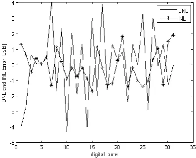
In the DAC we used current mirror as the output stage. The DAC supply their output currents directly to the current mirrors M1, M2, M3 (Fig. 7). Due to the channel modulation effects, the effective ratio of the drain current in M1 and M2 depends on drain-source voltages of both transistors, which are functions of the current fed into transistor M1 and the load transistor M3. Fig. 8 shows the output current of the DAC with differential nonlinearity and integral nonlinearity error in Fig. 9.
Figure 9. Differential and integral nonlinearity errors
Simulation result of the sum circuit at the lowers discriminator setting, when the shaper signals without offset as shown in Fig. 10. The discriminator generates two clock signals LL and LH that are input to the sum circuit, the output from the sum circuit is almost less than LL signal and bigger than LH. Fig. 11 shows the clock signal when shaper signal include offset.
IV. CONCLUSION
In this paper we have introduced architecture for a photon counting pixel detector readout with threshold correction for the comparators is implemented as a solution for the missing counting of the signal due to the offset problem. The additional circuits needed for this
architecture, leads to an increase in power consumption and in circuit area. It is implemented in a 120nm CMOS process and the presented results are based on simulations.
Figure 10. Simulation result of the circuit without offset input signal
Figure 11. Simulation result of the circuit with offset input signal
REFERENCES
[1] X. Llopart, M. Campbell, R. Dinapoli, D. san Segundo and E. Pernigotti, “Medipix2, a 64k pixel readout chip with 55µm square elements working in single photon counting mode,” IEEE
Transactions on Nuclear Science, vol. 49, pp. 2279-2283, Oct.
2002.
[2] B. E. Jonsson, Switched-Current Signal Processing and A/D
Conversion Circuits - Design and Implementation, Kluwer
Academic, 2000.
[3] S. Abdalla, B. Oelmann, M. O’Nils, and J. Lundgren, “Architecture and circuit design for colour x-ray pixel array detector read-out electronics,” in Proc. IEEE Norchip Conference, 2006, pp. 271-276.
[4] P. O’Connor, et al., “Readout electronics for a high-rate CSC detector,” in Proc. Fifth Workshop on Electronics for LHC
Experiments, Snowmass Colorado, Sep. 1999.
[5] new biasing
method for CMOS preamplifier-shaper,” in Proc. 7th IEEE Intl.
Conf. on Electronics Circuits and Systems, 2000, pp. 15-18.
[6] P. O’Connor and G. D. Geronimo, “Prospects for charge sensitive amplifiers in scaled CMOS,” in Proc. IEEE Nuclear Science Symp.
Conf. Record, Oct. 1999, vol. 1, pp. 89-93.
[7] M. Pedrali, et al., “Petric - A positron emission tomography readout integrated circuit,” IEEE Transactions on Nuclear Science, vol. 48, no. 3, pp. 479-484, Jun. 2001.
[8] L. T. Wurtz and W. P. Wheless, “Pulse shaping for low-noise, charge preamplifiers,” IEEE Transaction and Measurement, vol. 42, no. 5, pp. 942-946, Oct. 1993.
C. “A
[9] B. Oelmann, et al., “Robust window discriminator for photon-counting pixel detectors,” IEE Proceedings of Optoelectronics, vol. 149, no. 2, pp. 65-69, Apr. 2002.
[10] K. W. Current, “Current-Mode CMOS multiple-valued logic circuits,” IEEE Journal of Solid-State Circuits, vol. 29, no. 2, pp. 95-107, Feb. 1994.
[11] K. Bult and G. Geelen, “An inherently linear and compact MOST-only current-division technique,” IEEE Journal of Solid-State
Circuits, vol. 27, no. 12, pp. 1730-1735, Dec. 1992.
Suliman A. Abdalla obtained his B.Sc. in Electronics Engineering, 1999, Faculty of Engineering and Technology, University of Gezira, Sudan and Licentiate Degree in Electronics Engineering in 2007 from Mid Sweden University, Sundsvall, Sweden. Obtained his PhD in Electronics Engineering from Sudan Academy of Science 2014. He has been employed as an Electronics Engineer in the department of Electronics and Instrumentation at the Sudan Atomic Energy Commission (SAEC). His research focuses on the design of the read-out electronic interface between detectors and the intelligent data acquisition systems, the main read-out detector types of interest are photon counting pixel detectors for X-ray imaging
Marwa A. Mekki obtained her B.Sc. in Computer Engineering, 2000 from the Faculty of Engineering and Technology, University of Gezira, Sudan. She has obtained her M.Sc. Degree in Electronics Engineering in 2006 from the Mid Sweden University, Sundsvall, Sweden. She was a teaching assistant in the department of Computer Engineering, Faculty of Engineering and Technology since 2001, University of Gezira. She has become a lecturer in 2006 in the same faculty and university. She is doing her Ph.D. at the University of Gezira.