Vol.7 (2017) No. 3
ISSN: 2088-5334
The Structural and Electrical Properties of Nanostructures ZnO Thin
Films on Flexible Substrate
Nur Sa’adah Muhamad Sauki
#, Nur Amalina Muhamad
#, Fazlinashatul Suhaidah Zahid
#, Sukreen Hana
Herman
*, Zairi Ismael Rizman
##
Faculty of Electrical Engineering, Universiti Teknologi MARA, 81750 Masai, Johor, Malaysia E-mail: saadah1537@johor.uitm.edu.my, amalina0942@johor.uitm.edu.my, fazlina7803@johor.uitm.edu.my
*NANO-ElecTronic Centre,
Faculty of Electrical Engineering, Universiti Teknologi MARA, 40450 Shah Alam, Selangor, Malaysia E-mail: hana1617@salam.uitm.edu.my
#
Faculty of Electrical Engineering, Universiti Teknologi MARA, 23000 Dungun, Terengganu, Malaysia E-mail: zairi576@tganu.uitm.edu.my
Abstract— Zinc oxide (ZnO) thin films were deposited on Teflon substrates by radio frequency (RF) magnetron sputtering method at
different substrate temperature. The dependence of residual stress on the substrate temperature was investigated in this work due to the growth process, the bombardment of energetic particles and process heating to the deposited thin films. From field emission scanning electron microscope (FESEM) images, samples that deposited at various substrate temperatures consists nano-sized particles. The obtained X-ray diffraction (XRD) results, it suggested that ZnO thin film deposited at 40oC with highly c-axis oriented shows unstressed film compared to other thin films. Besides that, the ZnO thin films deposited at 40oC shows improved electrical properties.
Keywords— ZnO thin films; substrate temperatures; Teflon substrate; RF magnetron sputtering
I. INTRODUCTION
Research on a flexible substrate has been attracting much attention nowadays due to its attractive properties such as light weight and high resistance to impact damage. These properties make them suited for the fabrication of electronic device. Due to the poor thermal endurance of flexible substrate, zinc oxide (ZnO) is one of the materials that can be grown at lower deposition temperatures [1]. ZnO is naturally n-type direct band gap semiconductor materials that possess some great characteristics which are wide energy band gap, 3.37eV at room temperature and large free exciton binding energy, 60meV. It has the hexagonal crystalline structure of the wurtzite type and unit cell with a constant a = 3.24 Å and c = 5.19 Å as shown in Fig. 1.
Few flexible substrates found in literature such as polyethylene naphthalate (PEN), polyethylene terephthalate (PET), polycarbonate (PC) and polyethersulfone (PES) [3]-[6]. However, there is a lack of paper on growing ZnO thin films on polytetrafluoroethylene (Teflon) [7]. We choose polytetrafluoroethylene (Teflon) for our flexible substrates. The properties of Teflon make it a suitable choice for many
surface resistivity and high dielectric strength which means that the voltage that Teflon can withstand before it breaks down is high. In addition, Teflon has a low dissipation factor which is the percentage of electrical energy absorbed and lost when current is applied. A low dissipation factor indicates that the absorbed energy dissipated as heat is low. The high surface resistivity indicates the electrical resistance between opposite edges of a unit square on the surface of an insulating material. In this work, Teflon is chosen to be the substrate due to the availability in the market besides the above said favorable properties. Apart from that, Teflon can withstand corrosive environments and has a low dissipation factor.
The sputtering method is a process where atoms are ejected from a solid target material due to the bombardment of the target by energetic particles. There are a few steps to make a thin film using the sputtering method. The first step is to place substrate material in a vacuum chamber. Then, the air is removed, and the target material that desired to be deposited is released in the form of gas. The particle is bombarded with the energetic ions, inert gas ions (Ar+) typically. In the form of Ar+ 10 plasma, the negatively charged target material lines up on the substrate to form a thin film. Thin films can range in thickness from a few atoms to a few hundred atoms or molecules, which depend on the sputtering time [8]. It only happens when the kinetic energy of the incoming particles is much higher than conventional thermal energies. Sputtered atoms ejected from the target have a wide energy distribution, typically up to tens of eV (100,000 K) as can be seen in Fig. 2. The sputtered ions ejected from the target in straight lines and impact energetically on the substrates or vacuum chamber (causing resputtering) [9].
In this work, we choose RF magnetron sputtering as our method in order to deposit ZnO thin films on Teflon substrates.
Radio frequency (RF) magnetron sputtering method is used to deposit ZnO thin films on flexible due to its advantages ability to produce a uniform thin film which is good in adhesion and highly crystalline. In this paper, we report on the use of RF magnetron sputtering as a method in order to deposit a ZnO thin film on the flexible substrate at different substrate temperature for fabrication of high (002) oriented films. Apart from that, the residual stress was calculated in order to investigate the effect of the substrate deformation due to the growth process, the bombardment of energetic particles and process heating to the deposited thin films.
The flexible substrates technologies have recently attracted tremendous interest for the development of highly-demanding future product applications in efficient portable devices which are lightweight, foldable and wearable. However, there are some problems that need to be considered in the fabrication of the devices such as:
• The issue of obtaining high-quality thin films on polymer substrate at lower temperature (to suit poor thermal endurance of flexible substrates)
• Optimization of the deposition condition must be carried out to produce high-quality ZnO thin film
In this work, we focused on the growth of ZnO on Teflon substrate by using RF magnetron sputtering.
Fig. 2 Sputtering vacuum deposition process
II. MATERIAL AND METHOD
The deposition of ZnO film on Teflon substrate by RF magnetron sputtering methods and the characterization techniques that were used in this work are described in this section.
There are three steps in order to deposit ZnO thin films on Teflon substrate. The first step is the cleaning substrates, followed by deposition ZnO thin films and third steps are to material characterizations.
A. Teflon Substrates Cleaning Technique
Substrate cleaning technique is one of most important step in order to produce high-quality ZnO thin films. It is important to remove any organic and inorganic contamination on the substrate, prior to the deposition process. Contamination on the substrate may disturb the crystal growth and also negatively affect the performance of the fabricated device.
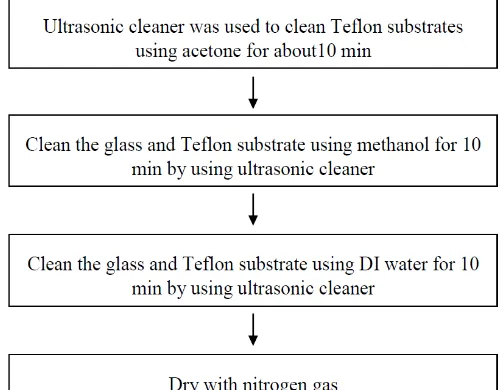
The Teflon substrates were cleaned by acetone in the ultrasonic cleaner for 10 minutes and followed by methanol for another 10 minutes in the ultrasonic cleaner. Then, the substrates were rinsed with deionized water (DI) in the ultrasonic cleaner for 10 minutes. Fig. 3 shows the flow of cleaning process.
B. Deposition of ZnO by RF Magnetron Sputtering
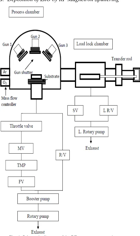
Fig. 4 Schematic diagram of the RF magnetron sputtering system
The deposition process was done by using RF magnetron sputtering (RSP-5004 (10SN06)). ZnO was deposited on polytetrafluoroethylene (Teflon) substrate using 4-inch in diameter 99.99% ZnO as the target. The details preparation, the background pressure in the sputtering chamber is 3.75x10⁻⁶ Torr, the working pressure was maintained at 5mTorr. For the first deposition, the samples were deposited for 1-hour deposition at different substrate temperatures, room temperature, 40oC, and 60oC. Table 1 shows the sputtering used in this work and Fig. 4 shows the schematic diagram of the RF magnetron sputtering system that was used in this work.
TABLEI
PARAMETERS OF DEPOSITION ZNOFILMS ON TEFLON SUBSTRATE OF RF MAGNETRON SPUTTERING
Background Pressure ~ 10-7 mTorr
Target ZnO
Substrate Temperature (oC) unheated, 40oC, 60oC
Ar (sccm) 45
O2 (sccm) 0
Sputtering Pressure (mTorr) 5
Process Time (sec) 1 hour
C. Characterizations of ZnO Thin Films
The characterizations are divided into two parts, which are structural and electrical properties.
D. Structural Properties
The structural properties were characterized by using the field-effect scanning electron microscope (FESEM) and the X-ray diffraction (XRD-Rigaku Ultima IV) used for the surface morphology and crystallinity properties respectively.
E. Surface Morphology
Surface morphology of the deposited ZnO thin films was measured using FESEM. The SEM image gives information of the thin film morphology and also the particle size of the thin film. Table 2 shows the parameters during the characterization.
TABLEIII
FESEMCHARACTERIZATION PARAMETERS
Magnification 80000-100000
Scale 100nm
Power 2 kV
F. Crystallinity
X-ray diffraction (XRD) is a versatile, non-destructive technique that reveals detailed information about the crystallographic structure of deposited thin film. When a monochromatic X-ray beam with wavelength, λ, is projected onto a crystalline material at an angle, θ, diffraction occurs only when the distance traveled by the rays reflected from successive planes differs by a complete number n of wavelengths as can be seen in Fig. 5.
Fig. 5 Bragg’s law
Bragg's Law refers to the simple equation as follows
nλ = 2d sinθ (1)
From the XRD collection data, the crystallite size can be calculated using Scherrer’s equation as follows
θ λ
cos
B K
D= (2)
where D is the crystallite size, K is a constant value 0.9 which depends mainly on the crystalline shape and indices,
λ
is the x-ray wavelength of 1.54Å, B is the full width at half maximum of the (002) plane wavelength in radian from XRD data, θ is the Bragg’s angle in degrees [10]. Apart from that, the stress can be calculated using biaxial strain model as follows [11] zz filmc
c
c
c
c
ε
∗
+
−
=
∂
13 12 11 33 2 132
)
(
)
(
2
(3)where the elastics constant Cij, data of single-crystalline ZnO have been used, C11 = 208.8GPa, C12 = 119.7GPa, C13 = 213.8GPa, εzz is the strain of the thin film. This yields the following numerical relation for the stress derived from XRD: σfilm = -233εzz. The strain (εzz) values can be calculated using equation as follows [12]
c
c
c
film zz−
=
ε
(4)where C is the unstrained lattice constant of ZnO, 5.206Å and Cfilm is the lattice parameters of analyzing film from XRD results.
G. Electrical Properties
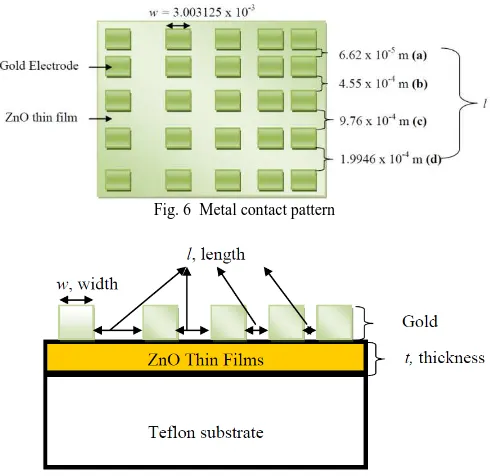
The electrical properties of the thin film were characterized using 2 point probes I-V measurement system (Keithley 2400). All thin films were deposited with gold (Au) metal contact for I-V measurement using a sputter coater (EMITECH K550X) with a thickness of 60nm and the width of the metal contact about 3.003x10⁻³m. The metal contacts were deposited at a deposition time of 4 minutes and sputtering current of 50 mA to achieve the thickness of 60 nm. The parameters for metal contact deposition are listed in Table 3.
TABLEIIIII SPUTTER COATER PARAMETERS
Metal Target Gold (Au)
Deposition Current 50mA
Deposition Time/Thickness 4 min / 60 nm
Deposition Ambient Argon
Sputtering Pressure 1 × 10⁻¹ mbar
Fig. 6 shows the metal contact patterns on the deposited ZnO thin films on Teflon substrate. Fig. 7 shows the device structure configurations for I-V measurements on the deposited ZnO thin films where w is the width, t is the thickness of the ZnO thin film and l is the length. This configuration is used in order to calculate the electrical resistivity and conductivity of deposited ZnO thin films on Teflon substrate. The electrical properties of deposited ZnO
thin films were measured by 2 point probes IV measurement system (Keithley 2400).
Fig. 6 Metal contact pattern
Fig. 7 Device structure configurations for I-V measurement
The thickness of ZnO thin films was measured using a surface profiler. With the IV data, the electrical resistivity and conductivity can be calculated using equations as follows = x wt I V ρ (4) = ρ σ 1 (5)
where ρ is resistivity, V is voltage, I is current, w is the width of Au, t is ZnO thin film thickness, x is the distance between electrodes and σ is conductivity.
III.RESULTS AND DISCUSSION
A. Structural Properties
poor interaction of metal and oxide layer as the annealing process increased the surface roughness and grain size [14].
Fig. 8 FESEM images of the deposited ZnO films at a) room temperature b) 40°C and c) 60°C
Fig. 9 shows the XRD pattern of deposited ZnO thin films at different substrate temperatures. It is observed that the deposited thin films at different substrate temperatures exhibits (002) diffraction structure that belongs to the hexagonal wurtzite type of ZnO (JCPDS #36-1451) [21], [22]. It illustrated that the (002) diffraction peak for deposited ZnO thin film at 40oC shows the highest peak intensity compared to other thin films, which indicates that the film is strongly c-axis oriented [13], [14]. However, when increased the substrate temperature, the (002) peak tends to decrease. Generally, it is said that higher substrate temperature will improve crystalline quality [15]-[17]. However, in our case, it is different. We predict that as the temperature increases, the Teflon substrate starts to deform. Even though the melting temperature of Teflon is about ~327oC and the setting temperature seems low enough not to cause deformation of the Teflon substrate, but during the sputtering process, the plasma temperature and the bombardment of the energetic particles on the substrate may increase the substrate temperature higher than the setting temperature.
Fig. 9 XRD patterns ZnO thin films at various substrate temperatures
The full width at half maximum (FWHM) of the (002) peak for all samples was ranged from 0.24oCto 0.42oC. It is observed that the FWHM decreases as the substrate temperature increases, which can be translated into increments of crystallite size as can be seen in Fig. 10.
From the XRD data, the average crystallite sizes for the thin films deposited at room temperature, 40oC and 60oC were between 21nm to 35.2nm in which the crystallite size increased with the substrate temperature.
Fig. 10 FWHM and crystallite size at various substrate temperatures
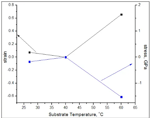
Aside from crystallite size, the stress and strain of the thin films also can be calculated using the obtained XRD data. The calculated of strain and stress values were plotted in Fig. 11.
Fig. 11 Strain and stress value at various substrate temperatures
The negative stress denotes that the film is in compression condition and the positive stress denotes the tensile state of the film. Generally, there are two types of stress, which are extrinsic stress and intrinsic stress. Extrinsic stress comes from the difference in the thermal expansion coefficients between the film and the substrate [18]. In this work, Teflon substrate shows high thermal expansion coefficient (135x10 -6K-1) and zinc oxide is (4.75x10⁻⁶K-1). The literature has been
c-axis orientation, higher peak intensity (002) will have more relaxed films and better crystalline quality which are at 40oC.
B. Electrical Properties
TABLEIVV
ELECTRICAL PROPERTIES AT VARIOUS SUBSTRATE TEMPERATURES
Substrate Temperature
Thickness (nm)
Conductivity (Sm-1)
Resistivity (Ωm)
27oC 590 0.81 X 10⁻² 1.24 X 10²
40oC 520 4.41 X 10⁻² 2.27 X 101
60oC 690 2.98 X 10⁻² 3.36 X 101
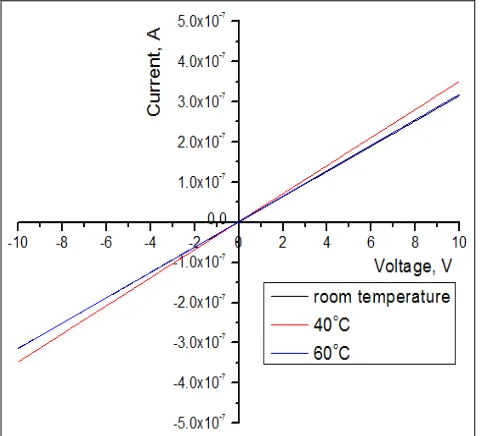
The current-voltage (I-V) curve of ZnO thin films deposited at different substrate temperatures was shown in Fig. 12. The results show all the thin films reveal ohmic behavior with Au metal contact. It can be seen that ZnO thin film deposited at 40oC shows the highest current intensity as the applied voltage changes from -10V to 10V. However, as the substrate temperature increased from 40oC to 60oC, the current intensity decreased.
The calculated value of the electrical resistivity and conductivity were tabulated in Table 4 and plotted in Fig. 11. It can be seen that the electrical conductivity increases as the substrate temperature increase from room temperature to 40oC. However, it decreases when the temperature increases to 60oC. This indicates that 40oC is the optimum temperature that would give higher conductivity.
Fig. 12 I-V curve at various substrate temperatures
The electrical resistivity of deposited ZnO thin film is the inverse of the electrical conductivity. Therefore, the electrical resistivity of the thin films decreases as the substrate temperature increases to 40oC and increases with the temperature as can be seen from Fig. 13. This is closely related to the ZnO thin film crystalline quality characterized by XRD in which the thin film deposited at 40oC has the highest crystalline quality. The better crystalline quality of material, the lesser imperfection in the atomic lattice. This imperfection hampers the movement of electrons which can be translated into higher resistivity of the material. This is portrayed by our results where the sample having the best
crystalline quality gives the highest conductivity, and when the crystalline quality reduced with increasing the substrate temperature, the conductivity also decreased.
Fig. 13 Electrical conductivity and resistivity at various substrate temperatures
IV.CONCLUSION
In conclusion, we have demonstrated the growth of ZnO thin films on Teflon substrate using RF magnetron sputtering method at different substrate temperature. FESEM images show that deposited ZnO thin films consist of nano-sized particles. From the obtained results, ZnO thin films deposited at 40oC shows highest (002) peak intensity. It can be concluded that with c-axis orientation will have relaxed films and improved electrical properties of ZnO thin films.
ACKNOWLEDGMENT
The author likes to express her thanks to Minister of Higher Education (MOHE) for financial support (600-RMI/RAGS 5/3 (198/2014)) and also to the Institute of Science Universiti Teknologi MARA for providing the laboratory facilities and technical support.
REFERENCES
[1] Y. Y. Liu, Y. Z. Yuan, C. F. Li, X. T. Gao, X. Z. Cao, and J. B. Li, “The structure and photoluminescence properties of RF-sputtered Films of ZnO on Teflon substrate,” Materials Letters, vol. 62, pp. 2907-2909, Jun. 2008.
[2] C. Y. Ren, S. H. Chiou, and C. S. Hsue, “Ga-doping effects on electronic and structural properties of wurtzite ZnO,” Physica B: Condensed Matter, vol. 349, pp. 136-142, Jun. 2004.
[3] M. G. S. Paz and R. R. Bon, “Indium tin oxide films deposited on polyethylene naphthalate substrates by radio frequency magnetron sputtering,” Thin Solid Films, vol. 517, pp. 2596-2601, Feb. 2009. [4] H. Liu and C. Lei, “Low-temperature deposited titanium-doped zinc
oxide thin films on the flexible PET substrate by DC magnetron sputtering,” Vacuum, vol. 86, pp. 483-486, Nov. 2011.
[5] L. Gong, J. Lu, and Z. Ye, “Transparent and conductive ga-doped ZnO films grown by RF magnetron sputtering on polycarbonate substrates,” Solar Energy Materials and Solar Cells, vol. 94, pp. 937-941, Jun. 2010.
[6] Y. C. Lin, M. Z. Chen, C. C. Kuo, and W. T. Yen, “Electrical and optical properties of ZnO: Al film prepared on polyethersulfone substrate by RF magnetron sputtering,” Colloids and Surfaces A: Physicochemical and Engineering Aspects, vol. 337, pp. 52-56, Apr. 2009.
[8] A. Fridman, Plasma Chemistry, 1st ed., Cambridge, England: Cambridge University Press, 2008.
[9] S. Lyon, “Materials selection for corrosion control,” International Materials Reviews, vol. 40, pp. 135-136, Jul. 2013.
[10] Y. Hu, O. K. Tan, J. S. Pan, H. Huang, and W. Cao, “The effects of annealing temperature on the sensing properties of low temperature nano-sized SrTiO3 oxygen gas sensor,” Sensors and Actuators B:
Chemical, vol. 108, pp. 244-249, Jul. 2005.
[11] B. Huang, G. He, and H. Yang, “Effects of annealing on excitonic properties of sputtered ZnO films at room temperature,” Journal of Optoelectronics and Advanced Materials, vol. 12, pp. 2369-2372, 2010.
[12] H. Y. Liu, G. S. Tang, F. Zeng, and F. Pan, “Influence of sputtering parameters on structures and residual stress of Aln films deposited by DC reactive magnetron sputtering at room temperature,” Journal of Crystal Growth, vol. 363, pp. 80-85, Jan. 2013.
[13] X. Ding and Y. Lai, “Electrical and optical properties of zinc oxide thin films deposited by magnetron sputtering,” ECS Transactions, vol. 34, pp. 577-582, Mar. 2011.
[14] J. J. Kim, J. H. Lee, J. Y. Lee, D. J. Lee, B. R. Jang, and H. S. Kim, “Characteristics of ZnO films deposited on plastic substrate at various RF sputtering powers,” Journal of Korean Physical Society, vol. 55, pp. 1910-1914, Nov. 2009.
[15] J. H. Park, J. M. Shin, S. Cha, J. W. Park, S. Jeong, H. K. Pak, and C. Cho, “Deposition-temperature effects on AZO thin films prepared by RF magnetron sputtering and their physical properties,” Journal of the Korean Physical Society, vol. 49, pp. S584-S588, Dec. 2006. [16] R. Ondo-Ndong, H. Z. Moussambi, H. Gnanga, A. Giani, and A.
Foucaran, “Optical properties of ZnO thin films deposed by RF
magnetron,” International Journal of Physical Sciences, vol. 10, pp.173-181, Mar. 2015.
[17] K. S. Kim, H. W. Kim, and N. H. Kim, “Structural characterization of ZnO films grown on SiO2 by the RF magnetron sputtering,”
Physica B: Condensed Matter, vol. 334, pp. 343-346, Jul. 2003. [18] R. S. Sreedharan, V. Ganesan, C. P. Sudarsanakumar, K. Bhavsar, R.
Prabhu, and V.P.P.M. Pillai, “Highly textured and transparent RF sputtered Eu2O3 doped ZnO films,” Nano Reviews, vol. 6, pp. 1-16,
Mar. 2015.
[19] A. K. Kalita and S. Karmakar, “Effect on particle size and microstrain due to iron doping on ZnO nanoparticle prepared by wet chemical method,” International Journal of Scientific Research, vol. 5, pp. 654-655, Apr. 2016.
[20] S. Kunj and K. Sreenivas, “Residual stress and defect content in magnetron sputtered ZnO films grown on unheated glass substrates,” Current Applied Physics, vol. 16, pp. 748-756, Jul. 2016.
[21] I. M. Yassin, A. Zabidi, M. S. A. M. Ali, N. M. Tahir, H. A. Hassan, H. Z. Abidin, and Z. I. Rizman, “Binary particle swarm optimization structure selection of nonlinear autoregressive moving average with exogenous inputs (NARMAX) model of a flexible robot arm,” International Journal on Advanced Science, Engineering and Information Technology, vol. 6, pp. 630-637, Oct. 2016.
![Fig. 1 Wurtzite structure of ZnO. Big and small spheres denote oxygen and zinc atoms respectively [2]](https://thumb-us.123doks.com/thumbv2/123dok_us/10036252.1990316/1.595.314.557.485.673/wurtzite-structure-small-spheres-denote-oxygen-atoms-respectively.webp)