Adv. Radio Sci., 9, 289–295, 2011 www.adv-radio-sci.net/9/289/2011/ doi:10.5194/ars-9-289-2011
© Author(s) 2011. CC Attribution 3.0 License.
Advances in
Radio Science
A modified prefix operator well suited for area-efficient brick-based
adder implementations
I. Rust and T. G. Noll
Chair of Electrical Engineering and Computer Systems, RWTH Aachen University, 52062 Aachen, Germany
Abstract. The implementation of integrated circuits be-comes more and more difficult in the Ultra-Deep-Submicron regime due to sub-wavelength lithography issues. An ap-proach called Brick-Based Design was recently proposed to eliminate the disadvantages of staying with the classical ap-proach to layout design. Prefix adders are a core component in a wide variety of applications due to their high speed and regular topology. In this paper, a modified prefix operator for prefix adders is proposed which is well suited for brick-style layout implementation and, in addition, offers an increase in efficiency. The proposed operator makes it possible to use a mirror gate for the generation of both generate and prop-agate signals, which exhibits a forbidden input signal com-bination. This “forbidden state” causes an increase in power dissipation due to transient short circuit currents. The effect of the forbidden state was quantified as part of a comparison against the classical prefix operator, based on 64-bit Sklan-sky adders implemented in a 40-nm CMOS technology. The effects of the forbidden state were found to be well accept-able. The implementation of the adder based on the proposed prefix operator reduces the area by 29% while increasing the power by 13% compared to one based on the classical oper-ator.
1 Introduction
The continuous reduction of feature sizes in nanometer scale technologies makes high-yield manufacturing at these tech-nology nodes a growing challenge.
This is because classical minimum-space design rules can not guarantee the effective usage of Resolution Enhance-ment Techniques (RETs) that are necessary to tackle the sub-wavelength lithography problems (Jhaveri et al., 2007). As a
Correspondence to: I. Rust
result, the yield is compromised and the circuit performance is reduced due to variability issues (Tong et al., 2006).
A straight-forward way to solve this problem is to use Design-For-Manufacturing (DFM or “Recommended”) rules, which allow to keep the classical approach to layout design, but usually cause a high area penalty.
As an alternative approach, it is possible to restrict allowed patterns for layout generation to a small subset highly opti-mized for lithography (“Restricted Patterning”) and, on the other hand, keep or even relax the corresponding layout de-sign rules (“Restricted Dede-sign Rules” with SRAM dede-sign rules as a well-known example (Jhaveri et al., 2007; Lieb-mann et al., 2009)). Using this design style, area savings of 15–25% compared to standard cells using DFM rules are ex-pected (Goering, 2007).
Figure 1 shows a layout comparison between minimum-spacing (MS) rules and DFM rules for an operator cell used in carry prefix adders, the area saving is as high as 35%.
Note: Layout pictures do not comply to real design rules to protect proprietary information.
In 2005, Kheterpal et al. (Kheterpal et al., 2005) proposed the Brick-Based Design approach, where a small set of logic primitives is mapped on cells called bricks, which are imple-mented using the Restricted Patterning approach. To ensure high yield manufacturability, the brick layout must comply to the following rules (Jhaveri et al., 2007, 2009; Tong et al., 2006; Liebmann et al., 2009; Kheterpal et al., 2005; Taylor and Pileggi, 2007):
– unidirectional use of poly-, diffusion and metal layers, – no jogs in poly layer,
– fixed pitch on poly/metal,
– high periodicity of layout structures.
Fast prefix adders based on the operator proposed by Brent-&Kung (Brent and Kung, 1982), layout shown in Fig. 1, are frequently used in a wide variety of applications due to their
290 I. Rust and T. G. Noll: A modified prefix operator well suited for area-efficient brick-based adder implementations with version 3.2 of the LTEX class copernicus.cls.
Date: 9 February 2011
A Modified Prefix Operator Well Suited for Area-Efficient
Brick-Based Adder Implementations
Ingo Rust and Tobias G. Noll
Chair of Electrical Engineering and Computer Systems RWTH Aachen University, Germany
{rust,tgn}@eecs.rwth-aachen.de
Abstract. The implementation of integrated circuits be-comes more and more difficult in the Ultra-Deep-Submicron regime due to sub-wavelength lithography issues. An ap-proach called Brick-Based Design was recently proposed to eliminate the disadvantages of staying with the classical ap-proach to layout design. Prefix adders are a core component in a wide variety of applications due to their high speed and regular topology. In this paper, a modified prefix operator for prefix adders is proposed which is well suited for brick-style layout implementation and, in addition, offers an increase in efficiency. The proposed operator makes it possible to use a mirror gate for the generation of both generate and prop-agate signals, which exhibits a forbidden input signal com-bination. This “forbidden state” causes an increase in power dissipation due to transient short circuit currents. The effect of the forbidden state was quantified as part of a comparison against the classical prefix operator, based on 64-bit Sklan-sky adders implemented in a 40-nm CMOS technology. The effects of the forbidden state were found to be well accept-able. The implementation of the adder based on the proposed prefix operator reduces the area by 29% while increasing the power by 13% compared to one based on the classical oper-ator.
1 Introduction
The continuous reduction of feature sizes in nanometer scale technologies makes high-yield manufacturing at these tech-nology nodes a growing challenge.
This is because classical minimum-space design rules can not guarantee the effective usage of Resolution Enhance-ment Techniques (RETs) that are necessary to tackle the sub-wavelength lithography problems (Tejas Jhaveri et al., 2007). As a result, the yield is compromised and the circuit perfor-mance is reduced due to variability issues (K.Y. Tong et al., 2006).
A straight-forward way to solve this problem is to use Design-For-Manufacturing (DFM or “Recommended”) rules, which allow to keep the classical approach to layout design, but usually cause a high area penalty.
As an alternative approach, it is possible to restrict allowed patterns for layout generation to a small subset highly opti-mized for lithography (“Restricted Patterning”) and, on the other hand, keep or even relax the corresponding layout de-sign rules (“Restricted Dede-sign Rules” with SRAM dede-sign rules as a well-known example (Tejas Jhaveri et al., 2007; L. Liebmann et al., 2009)). Using this design style, area sav-ings of 15-25% compared to standard cells using DFM rules are expected (Richard Goering).
Fig. 1 shows a layout comparison between minimum-spacing (MS) rules and DFM rules for an operator cell used in carry prefix adders, the area saving is as high as 35%.
DFM rules minimum spacing rules
A: −35%
Fig. 1.B&K prefix operator: MS vs. DFM rules
Fig. 1. B&K prefix operator: MS vs. DFM rules.
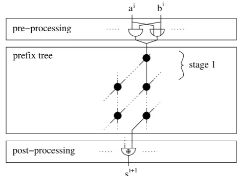
high speed and high regularity compared to carry-lookahead adders. All prefix adders consist of a pre-processing block, prefix tree and post-processing block (see Fig. 2). Different variants differ only in the topology of their prefix tree (Patil et al., 2007). The pre-processing block computes generate (gi), transmit (ti) and propagate (pi) signals for every weight i based on the corresponding input bits ai andbi. In the prefix tree these signals are used to compute carry bitsci in every weighti. These carrys are fed to the post-processing block which uses them together with the propagate signals to generate the sum bitssi.
In Kheterpal et al. (2005), a Kogge-Stone adder was re-alized with a design-specific brick set and compared to an implementation based on a commercial 90-nm standard cell library. Results show that by using 8 different bricks, de-lay is only increased by 6% and area only increased by 15% compared to the standard-cell-based implementation without layout pattern restrictions despite the much more limited lay-out pattern set allowed in a brick based approach.
In this paper, a modified prefix operator, inherently, well suited for implementation in a brick-style fashion is pro-posed. Based on the properties of the brick-realization of the operator, a complete brick set for the flexible realization of arbitrary prefix adders is developed and implemented.
The paper is organized as follows: in Sect. 2 the mirror gate used for the implementation of the proposed operator is described and the motivation for its usage for brick-based adder implementations is presented. Section 3 presents the derivation of the modified prefix operator. A complete brick set for the implementation of arbitrary adders based on the proposed operator is developed in Sect. 4. In Sect. 5 a quan-titative comparison between the proposed operator and the one from Brent&Kung is presented, based on 64-bit Sklan-sky adder implementations. The effect of the forbidden state
2 I. Rust, T.G. Noll: A Modified Prefix Operator Well Suited for Area-Efficient Brick-Based Adder Implementations
Note: Layout pictures do not comply to real design rules to protect proprietary information.
In 2005, Kheterpal et al. (V. Kheterpal et al., 2005) proposed the Brick-Based Design approach, where a small set of logic primitives is mapped on cells called bricks, which are imple-mented using the Restricted Patterning approach. To ensure high yield manufacturability, the brick layout must comply to the following rules (Tejas Jhaveri et al., 2007; K.Y. Tong et al., 2006; L. Liebmann et al., 2009; V. Kheterpal et al., 2005; B. Taylor and L. Pileggi, 2007; Tejas Jhaveri et al., 2009):
– unidirectional use of poly-, diffusion and metal layers,
– no jogs in poly layer,
– fixed pitch on poly/metal,
– high periodicity of layout structures.
Fast prefix adders based on the operator proposed by Brent-&Kung (R. Brent and H. Kung, 1982), layout shown in Fig. 1, are frequently used in a wide variety of applica-tions due to their high speed and high regularity compared to carry-lookahead adders. All prefix adders consist of a pre-processing block, prefix tree and post-processing block (see Fig. 2). Different variants differ only in the topology of their prefix tree (Patil et al., 2007). The pre-processing block computes generate (gi), transmit (ti) and propagate (pi) sig-nals for every weightibased on the corresponding input bits
ai andbi. In the prefix tree these signals are used to com-pute carry bitsci in every weighti. These carrys are fed to the post-processing block which uses them together with the propagate signals to generate the sum bitssi.
ai bi
si+1 pre−processing
stage 1
post−processing prefix tree
Fig. 2.General building blocks of prefix adders
In (V. Kheterpal et al., 2005), a Kogge-Stone adder was re-alized with a design-specific brick set and compared to an implementation based on a commercial 90-nm standard cell library. Results show that by using 8 different bricks, de-lay is only increased by 6% and area only increased by 15%
compared to the standard-cell-based implementation without layout pattern restrictions despite the much more limited lay-out pattern set allowed in a brick based approach.
In this paper, a modified prefix operator, inherently, well suited for implementation in a brick-style fashion is pro-posed. Based on the properties of the brick-realization of the operator, a complete brick set for the flexible realization of arbitrary prefix adders is developed and implemented. The paper is organized as follows: In section 2 the mir-ror gate used for the implementation of the proposed oper-ator is described and the motivation for its usage for brick-based adder implementations is presented. Section 3 presents the derivation of the modified prefix operator. A complete brick set for the implementation of arbitrary adders based on the proposed operator is developed in section 4. In section 5 a quantitative comparison between the proposed operator and the one from Brent&Kung is presented, based on 64-bit Sklansky adder implementations. The effect of the forbidden state of the proposed operator at the presence of variability is evaluated. Section 6 concludes this work.
2 Gate for brick implementation
The implementation of carry-generating gates in carry-look-ahead adders using Branch-Based Logic (BBL) is a well-known and frequently used approach ((A. Neve, D. Flandre, H.Schettler, T. Ludwig and G. Hellner, 2002; J. Masgonty, C. Arm and C. Piguet, 1991)). In BBL gates, the topologies for p- and n-channel networks are created separately by form-ing the gate’s pull-up and pull-down equations in a sum-of-product fashion (J. Masgonty, C. Arm and C. Piguet, 1991). As a result, every connection from supply to output and from output to ground forms a simple, straight transistor stack without internal branches, so intermediate parasitic capaci-tances are reduced to a minimum. This leads to a smaller delay and possibly to a smaller power dissipation.
The well known formula
ci+1=gi+ti·ci (1)
with
gi=ai·bi, ti=ai+bi (2) describes the computation of the carry in bit positioni+ 1
depending on the local generate and transmit condition and the incoming carry in bit positioni. Equation 1 can be gen-eralized to the form
Gi:k=Gi:j+Ti:j·Gj−1:k, (3) where Gi:j and Ti:j denote the group carry generate and group carry propagate signals for weighti down to weight
j, respectively (Zimmermann, 1997). The inverted form of equation 1
ci+1=gi+ti·ci (4)
Fig. 2. General building blocks of prefix adders.
of the proposed operator at the presence of variability is eval-uated. Section 6 concludes this work.
2 Gate for brick implementation
The implementation of carry-generating gates in carry-look-ahead adders using Branch-Based Logic (BBL) is a well-known and frequently used approach (Neve et al., 2002; Mas-gonty et al., 1991). In BBL gates, the topologies for p- and n-channel networks are created separately by forming the gate’s pull-up and pull-down equations in a sum-of-product fashion (Masgonty et al., 1991).
As a result, every connection from supply to output and from output to ground forms a simple, straight transistor stack without internal branches, so intermediate parasitic ca-pacitances are reduced to a minimum. This leads to a smaller delay and possibly to a smaller power dissipation.
The well known formula
ci+1=gi+ti·ci (1)
with
gi=ai·bi, ti=ai+bi (2) describes the computation of the carry in bit positioni+1 depending on the local generate and transmit condition and the incoming carry in bit position i. Equation (1) can be generalized to the form
Gi:k=Gi:j+Ti:j·Gj−1:k, (3) where Gi:j and Ti:j denote the group carry generate and group carry propagate signals for weighti down to weight j, respectively (Zimmermann, 1997). The inverted form of Eq. (1)
ci+1=gi+ti·ci (4)
I. Rust and T. G. Noll: A modified prefix operator well suited for area-efficient brick-based adder implementations 291 I. Rust, T.G. Noll: A Modified Prefix Operator Well Suited for Area-Efficient Brick-Based Adder Implementations 3
can be implemented using an and-or-invert gate (aoi). Be-cause of the fact that the conditions
gi=ai·bi= 1andti=ai+bi= 0 (5) can never happen simultaneously at the outputs of the adders preprocessing block (neglecting delay effects for now), the n-channel topology of the aoi gate can also be used in the p-channel part, yielding a symmetric mirror gate which also is a BBL-style gate ((A. Neve, D. Flandre, H.Schettler, T. Lud-wig and G. Hellner, 2002), Fig. 3). The fact represented in equation 5 motivates the usage of transmit conditionsti(A. Weinberger and J.L. Smith, 1958) instead of the more com-mon propagate conditionspi (R. Brent and H. Kung, 1982) where(gi= 1,pi=ai⊕bi= 0)is possible, preventing the usage of a mirror gate.
Moreover, the dual expression
ci+1=gi·(ti+ci) (6)
can be implemented using the mirror gate by interchanging
gi withti,ti withgi and utilizing the absence of the input state(gi= 0,ti= 1). Normally it would be necessary to im-plement equation 6 using an or-and-invert gate (oai). Fig. 3 shows the corresponding transistor schematics, de-picting two alternative implementations for an oai and an aoi gate, respectively. Fig. 3 a) shows the mirror gate with signal names corresponding to the use as a replacement for an aoi or an oai gate, respectively. Fig. 3 b) and Fig. 3 c) depict dif-ferent versions of complex aoi and oai gates. Fig. 3 c) shows delay-enhanced versions which trade an additional transistor for the absence of additional branches in the n- or p-channel topologies, which is inherent in the BBL mirror gate version.
G G T G G T G T G G T G G G G G T G G G T G T G G G G T G G G G T T G G G i:k j−1:k i:j i:j i:j i:k i:j i:j j−1:k j−1:k i:j i:j i:j i:j j−1:k j−1:k i:j i:j i:k i:j j−1:k j−1:k i:j i:j i:j i:j j−1:k j−1:k i:j i:j i:k i:j j−1:k i:j i:j i:j i:k i:k G (c) (b) (a) aoi oai
Fig. 3.Gate schematic comparison: a) mirror gate b) 6-transistor complex gates c) 7-transistor complex gates
Fig. 4 shows a comparison of the layout implementation of the mirror gate and the six-transistor variant of the aoi gate.
The supply nodes of the mirror gate are located directly at the cell boundary in a symmetrical fashion, which is not the case for the aoi gate. This makes it possible to share the supply nodes between adjacent mirror gates, hence, reducing the area per gate significantly (-29% in 40-nm). The result-ing cell rows are not only very dense, but also highly regular without any poly jog. In contrast, the seven-transistor vari-ants of aoi and oai can also share supply contacts over cell boundaries, but not without poly jogs.
A comparison using a 90-nm technology shows that the pair delay of the mirror gate is approximately 20% smaller com-pared to a cascade of 6-transistor aoi and oai gates, depend-ing on the fanout (post layout simulation/slow conditions).
00 00 00 00 00 00 00 00 00 00 00 00 00 00 00 00 00 00 00 11 11 11 11 11 11 11 11 11 11 11 11 11 11 11 11 11 11 11 00 00 00 00 00 00 00 00 00 00 00 00 00 00 00 00 00 00 00 11 11 11 11 11 11 11 11 11 11 11 11 11 11 11 11 11 11 11 0 0 0 0 0 0 0 0 0 0 0 0 0 0 0 0 0 0 0 1 1 1 1 1 1 1 1 1 1 1 1 1 1 1 1 1 1 1 00 00 00 00 00 11 11 11 11 11 00 00 00 00 11 11 11 11 00 00 00 00 00 00 00 00 00 00 00 00 00 00 00 00 00 00 00 11 11 11 11 11 11 11 11 11 11 11 11 11 11 11 11 11 11 11 00 00 00 00 00 00 00 00 00 00 00 00 00 00 00 00 00 00 00 11 11 11 11 11 11 11 11 11 11 11 11 11 11 11 11 11 11 11 0 0 0 0 0 0 0 0 0 0 0 0 0 0 0 0 0 0 0 1 1 1 1 1 1 1 1 1 1 1 1 1 1 1 1 1 1 1
Gj−1:k Gi:j Ti:j
Gj−1:k Ti:j Gi:j
i:k G
Gj−1:k Ti:j Gi:j i:k G
Ti:j Gj−1:k Gi:j
Area: −29% Vdd Gnd Vdd Vdd Gnd Gnd Gnd = supply = contact = diffusion = metal = poly i:k G mirror gate aoi 0000 0000 0000 0000 0000 0000 0000 0000 0000 0000 0000 0000 0000 0000 1111 1111 1111 1111 1111 1111 1111 1111 1111 1111 1111 1111 1111 1111 0000000 0000000 0000000 0000000 0000000 0000000 0000000 1111111 1111111 1111111 1111111 1111111 1111111 1111111 0000 0000 0000 0000 0000 0000 0000 0000 0000 0000 0000 0000 0000 0000 1111 1111 1111 1111 1111 1111 1111 1111 1111 1111 1111 1111 1111 1111 i:k G
Fig. 4.Mask layout diagrams
3 Modified Prefix Operator
The main disadvantage of the described mirror gate is the existence of a so-called forbidden input state. If the forbid-den input combination is applied, a short current flows from supply to ground. Taking a closer look at the mirror gate shown in Fig. 3 a), it becomes clear that this happens for
Ti:j= 0,Gi:j= 1in the version corresponding to an aoi gate and forTi:j= 1,Gi:j= 0in the version corresponding to an oai gate.
As mentioned earlier, it is always possible to use the mirror gate in the first stage of the prefix graph directly after the preprocessing (see Fig. 2), because the forbidden input state is not present in the signal pairsgi,tiandgi,ti, respectively (eq. 5) and the inputs of all prefix operators in this stage are connected only to those signal pairs (wired to the operators according to the identitiesgi=Gi:iandti=Ti:i).
The “•”-operator introduced by Brent and Kung (R. Brent
Fig. 3. Gate schematic comparison: (a) mirror gate, (b) 6-transistor complex gates, (c) 7-transistor complex gates.
can be implemented using an and-or-invert gate (aoi). Be-cause of the fact that the conditions
gi=ai·bi=1 andti=ai+bi=0 (5) can never happen simultaneously at the outputs of the adders preprocessing block (neglecting delay effects for now), the n-channel topology of the aoi gate can also be used in the p-channel part, yielding a symmetric mirror gate which also is a BBL-style gate (Neve et al., 2002, Fig. 3). The fact repre-sented in Eq. (5) motivates the usage of transmit conditions ti (Weinberger and Smith, 1958) instead of the more com-mon propagate conditionspi (Brent and Kung, 1982) where (gi=1,pi=ai⊕bi=0)is possible, preventing the usage of a mirror gate.
Moreover, the dual expression
ci+1=gi·(ti+ci) (6)
can be implemented using the mirror gate by interchanging gi withti,ti withgi and utilizing the absence of the input
state(gi=0,ti=1). Normally it would be necessary to
im-plement Eq. (6) using an or-and-invert gate (oai).
Figure 3 shows the corresponding transistor schematics, depicting two alternative implementations for an oai and an aoi gate, respectively. Figure 3a shows the mirror gate with signal names corresponding to the use as a replacement for an aoi or an oai gate, respectively. Figure 3b and Fig. 3c depict different versions of complex aoi and oai gates. Fig-ure 3c shows delay-enhanced versions which trade an addi-tional transistor for the absence of addiaddi-tional branches in the n- or p-channel topologies, which is inherent in the BBL mir-ror gate version.
Figure 4 shows a comparison of the layout implementa-tion of the mirror gate and the six-transistor variant of the aoi gate. The supply nodes of the mirror gate are located directly at the cell boundary in a symmetrical fashion, which is not the case for the aoi gate. This makes it possible to share the
I. Rust, T.G. Noll: A Modified Prefix Operator Well Suited for Area-Efficient Brick-Based Adder Implementations 3
can be implemented using an and-or-invert gate (aoi). Be-cause of the fact that the conditions
gi=ai·bi= 1andti=ai+bi= 0 (5) can never happen simultaneously at the outputs of the adders preprocessing block (neglecting delay effects for now), the n-channel topology of the aoi gate can also be used in the p-channel part, yielding a symmetric mirror gate which also is a BBL-style gate ((A. Neve, D. Flandre, H.Schettler, T. Lud-wig and G. Hellner, 2002), Fig. 3). The fact represented in equation 5 motivates the usage of transmit conditionsti (A. Weinberger and J.L. Smith, 1958) instead of the more com-mon propagate conditionspi(R. Brent and H. Kung, 1982) where(gi= 1,pi=ai⊕bi= 0) is possible, preventing the usage of a mirror gate.
Moreover, the dual expression
ci+1=gi·(ti+ci) (6)
can be implemented using the mirror gate by interchanging
gi withti,ti withgi and utilizing the absence of the input state(gi= 0,ti= 1). Normally it would be necessary to im-plement equation 6 using an or-and-invert gate (oai). Fig. 3 shows the corresponding transistor schematics, de-picting two alternative implementations for an oai and an aoi gate, respectively. Fig. 3 a) shows the mirror gate with signal names corresponding to the use as a replacement for an aoi or an oai gate, respectively. Fig. 3 b) and Fig. 3 c) depict dif-ferent versions of complex aoi and oai gates. Fig. 3 c) shows delay-enhanced versions which trade an additional transistor for the absence of additional branches in the n- or p-channel topologies, which is inherent in the BBL mirror gate version.
G G T G G T G T G G T G G G G G T G G G T G T G G G G T G G G G T T G G G i:k j−1:k i:j i:j i:j i:k i:j i:j j−1:k j−1:k i:j i:j i:j i:j j−1:k j−1:k i:j i:j i:k i:j j−1:k j−1:k i:j i:j i:j i:j j−1:k j−1:k i:j i:j i:k i:j j−1:k i:j i:j i:j i:k i:k G c) b) a) aoi oai
Fig. 3.Gate schematic comparison: a) mirror gate b) 6-transistor complex gates c) 7-transistor complex gates
Fig. 4 shows a comparison of the layout implementation of the mirror gate and the six-transistor variant of the aoi gate.
The supply nodes of the mirror gate are located directly at the cell boundary in a symmetrical fashion, which is not the case for the aoi gate. This makes it possible to share the supply nodes between adjacent mirror gates, hence, reducing the area per gate significantly (-29% in 40-nm). The result-ing cell rows are not only very dense, but also highly regular without any poly jog. In contrast, the seven-transistor vari-ants of aoi and oai can also share supply contacts over cell boundaries, but not without poly jogs.
A comparison using a 90-nm technology shows that the pair delay of the mirror gate is approximately 20% smaller com-pared to a cascade of 6-transistor aoi and oai gates, depend-ing on the fanout (post layout simulation/slow conditions).
00 00 00 00 00 00 00 00 00 00 00 00 00 00 00 00 00 00 00 11 11 11 11 11 11 11 11 11 11 11 11 11 11 11 11 11 11 11 00 00 00 00 00 00 00 00 00 00 00 00 00 00 00 00 00 00 00 11 11 11 11 11 11 11 11 11 11 11 11 11 11 11 11 11 11 11 0 0 0 0 0 0 0 0 0 0 0 0 0 0 0 0 0 0 0 1 1 1 1 1 1 1 1 1 1 1 1 1 1 1 1 1 1 1 00 00 00 00 00 11 11 11 11 11 00 00 00 00 11 11 11 11 00 00 00 00 00 00 00 00 00 00 00 00 00 00 00 00 00 00 00 11 11 11 11 11 11 11 11 11 11 11 11 11 11 11 11 11 11 11 00 00 00 00 00 00 00 00 00 00 00 00 00 00 00 00 00 00 00 11 11 11 11 11 11 11 11 11 11 11 11 11 11 11 11 11 11 11 0 0 0 0 0 0 0 0 0 0 0 0 0 0 0 0 0 0 0 1 1 1 1 1 1 1 1 1 1 1 1 1 1 1 1 1 1 1
Gj−1:k Gi:j Ti:j
Gj−1:k Ti:j Gi:j
i:k G
Gj−1:k Ti:j Gi:j i:k G
Ti:j Gj−1:k Gi:j
Area: −29% Vdd Gnd Vdd Vdd Gnd Gnd Gnd = supply = contact = diffusion = metal = poly i:k G mirror gate aoi 0000 0000 0000 0000 0000 0000 0000 0000 0000 0000 0000 0000 0000 0000 1111 1111 1111 1111 1111 1111 1111 1111 1111 1111 1111 1111 1111 1111 0000000 0000000 0000000 0000000 0000000 0000000 0000000 1111111 1111111 1111111 1111111 1111111 1111111 1111111 0000 0000 0000 0000 0000 0000 0000 0000 0000 0000 0000 0000 0000 0000 1111 1111 1111 1111 1111 1111 1111 1111 1111 1111 1111 1111 1111 1111 i:k G
Fig. 4.Mask layout diagrams
3 Modified Prefix Operator
The main disadvantage of the described mirror gate is the existence of a so-called forbidden input state. If the forbid-den input combination is applied, a short current flows from supply to ground. Taking a closer look at the mirror gate shown in Fig. 3 a), it becomes clear that this happens for
Ti:j= 0,Gi:j= 1in the version corresponding to an aoi gate and forTi:j= 1,Gi:j= 0in the version corresponding to an oai gate.
As mentioned earlier, it is always possible to use the mirror gate in the first stage of the prefix graph directly after the preprocessing (see Fig. 2), because the forbidden input state is not present in the signal pairsgi,tiandgi,ti, respectively (eq. 5) and the inputs of all prefix operators in this stage are connected only to those signal pairs (wired to the operators according to the identitiesgi=Gi:iandti=Ti:i).
The “•”-operator introduced by Brent and Kung (R. Brent
Fig. 4. Mask layout diagrams.
supply nodes between adjacent mirror gates, hence, reducing the area per gate significantly (−29% in 40-nm). The result-ing cell rows are not only very dense, but also highly regular without any poly jog. In contrast, the seven-transistor vari-ants of aoi and oai can also share supply contacts over cell boundaries, but not without poly jogs.
A comparison using a 90-nm technology shows that the pair delay of the mirror gate is approximately 20% smaller compared to a cascade of 6-transistor aoi and oai gates, de-pending on the fanout (post layout simulation/slow condi-tions).
3 Modified prefix operator
The main disadvantage of the described mirror gate is the existence of a so-called forbidden input state. If the for-bidden input combination is applied, a short current flows from supply to ground. Taking a closer look at the mirror gate shown in Fig. 3a, it becomes clear that this happens for Ti:j=0,Gi:j=1 in the version corresponding to an aoi gate and forTi:j=1,Gi:j=0 in the version corresponding to an
oai gate.
As mentioned earlier, it is always possible to use the mirror gate in the first stage of the prefix graph directly after the preprocessing (see Fig. 2), because the forbidden input state is not present in the signal pairsgi,ti andgi,ti, respectively
(Eq. 5) and the inputs of all prefix operators in this stage are connected only to those signal pairs (wired to the operators according to the identitiesgi=Gi:iandti=Ti:i).
The “
4 I. Rust and T. G. Noll: A modified prefix operator well suited for area-efficient brick-based adder implementations
Table 1. Application of “•”-operator to output of preprocessing.
gi ti gi−1 ti−1 Gi:i−1 Ti:i−1
0 0 0 0 0 0
0 0 0 1 0 0
0 0 1 1 0 0
0 1 0 0 0 0
0 1 0 1 0 1
0 1 1 1 1 1
1 1 0 0 1 0
1 1 0 1 1 1
1 1 1 1 1 1
to the fact that the carry is already generated because of
Gi:i−1=1 (?).
To exploit this fact, a modified prefix operator, denoted as
“”, is introduced and defined as follows
(g,t )(g,ˆ t )ˆ =(g+t· ˆg,g+t· ˆt ). (8)
Comparing the truth table of the modified operator with the
truth table of the “•”-operator in Table ??, the only
dif-ference is the value of Ti:i−1 in the marked row, which
is one for the modified operator. So the forbidden state
(Gi:i−1=1,Ti:i−1 =0) is replaced by the allowed state
(G˜i:i−1=1,T˜i:i−1=1)which is equivalent regarding carry
generation. The fact that the signal pair(G˜i:i−1,T˜i:i−1)can
now only take the values(0,0),(0,1)and(1,1)(sharing this
property with(gi,ti)) means that input and output pairs of
Table ?? both do not contain the forbidden state. This is a prerequisite to use the mirror gate at any position inside a prefix tree.
The modified operator, “”, to be used as a replacement
for “•” exhibits the following properties
– ci+1= ˜Gi∀i
– “” must be associative
– “” must be idempotent
– G˜i=1,T˜i=0 must never occur
The first three properties can be proved in analogy to “•”, so
these proves are omitted. The last property can be proved by contradiction as follows
˜
Gi:k=1,T˜i:k=0
⇒ ˜Gi:j+ ˜Ti:j· ˜Gj−1:k=1
˜
Gi:j+ ˜Ti:j· ˜Tj−1:k=0
⇒ ˜Gj−1:k=1,T˜j−1:k=0
j →k+2:
⇒gk+1+tk+1·gk=1, gk+1+tk+1·tk=0,
⇒gk=ak·bk=1,tk=ak+bk=0 qed.
4 I. Rust, T.G. Noll: A Modified Prefix Operator Well Suited for Area-Efficient Brick-Based Adder Implementations
and H. Kung, 1982) is, for any Boolean variablesg,t,gˆand ˆ
t, defined as
(g,t)•(ˆg,tˆ) = (g+t·g,tˆ ·tˆ). (7)
Using the “•”-operator on the signal pairs generated in the pre-processing block creates the forbidden state at the inputs of the following operator cells (Tab. 1).
The forbidden state(Gi:i−1= 1,Ti:i−1= 0)appears at the
gi ti gi−1 ti−1 Gi:i−1 Ti:i−1
0 0 0 0 0 0
0 0 0 1 0 0
0 0 1 1 0 0
0 1 0 0 0 0
0 1 0 1 0 1
0 1 1 1 1 1
1 1 0 0 1 0
1 1 0 1 1 1
1 1 1 1 1 1
Table 1.Application of “•”-operator to output of preprocessing
row marked in gray, because a carry would be generated at weighti, but none would be transmitted from weight i−1. Taking a closer look atGi:i−1andTi:i−1, it is obvious that Ti:i−1 is irrelevant for the process of carry generation due to the fact that the carry is already generated because of Gi:i−1= 1(R. Brent and H. Kung, 1982).
To exploit this fact, a modified prefix operator, denoted as “”, is introduced and defined as follows
(g,t)(ˆg,ˆt) = (g+t·ˆg,g+t·ˆt). (8)
Comparing the truth table of the modified operator with the truth table of the “•”-operator in Tab. 1, the only dif-ference is the value of Ti:i−1 in the marked row, which is one for the modified operator. So the forbidden state (Gi:i−1= 1,Ti:i−1= 0) is replaced by the allowed state ( ˜Gi:i−1= 1,T˜i:i−1= 1)which is equivalent regarding carry generation. The fact that the signal pair( ˜Gi:i−1,T˜i:i−1)can now only take the values(0,0),(0,1)and(1,1)(sharing this property with(gi,ti)) means that input and output pairs of Tab. 1 both do not contain the forbidden state. This is a pre-requisite to use the mirror gate at any position inside a prefix tree.
The modified operator, “”, to be used as a replacement for “•” exhibits the following properties
– ci+1= ˜Gi∀i
– “” must be associative
– “” must be idempotent
– G˜i= 1,T˜i= 0must never occur
The first three properties can be proved in analogy to “•”, so these proves are omitted. The last property can be proved by contradiction as follows
˜
Gi:k= 1,T˜i:k= 0 ⇒G˜i:j+ ˜Ti:j·G˜j−1:k= 1
˜
Gi:j+ ˜Ti:j·T˜j−1:k= 0 ⇒G˜j−1:k= 1,T˜j−1:k= 0 j→k+ 2 :
⇒gk+1+tk+1·gk= 1, gk+1+tk+1·tk= 0,
⇒gk=ak·bk= 1,tk=ak+bk= 0qed.
4 Derivation of brick set
Now a brick set for the realization of arbitrary prefix adders is derived based on the presented modified prefix operator. It is evident that the implementation of the operator cell(s) is crucial for the adder efficiency, which strongly suggests the layout adaption of the remaining cells to the layout of an op-erator cell which is implemented as efficiently as possible. In modern deep-sub-micron CMOS technologies for which a brick-based design style is advantageous, the ratio of wiring capacitance to gate capacitance is ever increasing (Veen-drick, 2000). To accommodate this fact, the bit slice width should be kept at a minimum. Therefore, and due to the shareable supply contacts of the mirror gate depicted in Fig. 4, the operator cell contains two mirror gates on top of each other as shown in Fig. 5. To show the effect of supply contact sharing, two operator cells are cascaded horizontally, which is indicated by the dashed boxes in the operator examples. Implemented in a state-of-the-art 40-nm technology, the re-sulting cell pitch of the proposed version is only 0.48µm at a cell height of 1.33µm, using minimum-sized transistors.
A: −29% ’ ’ ’ ’
Fig. 5.vs.•: comparison of layouts (MS rules)
Fig. 5 shows the comparison of “” implemented using mir-ror gates and “•” using the seven-transistor aoi gate for Gi in combination with a nand-gate producingTi. Layouts are
Fig. 5.vs.•: comparison of layouts (MS rules).
4 Derivation of brick set
Now a brick set for the realization of arbitrary prefix adders is derived based on the presented modified prefix operator.
It is evident that the implementation of the operator cell(s) is crucial for the adder efficiency, which strongly suggests the layout adaption of the remaining cells to the layout of an operator cell which is implemented as efficiently as possible. In modern deep-sub-micron CMOS technologies for which a brick-based design style is advantageous, the ratio of wiring capacitance to gate capacitance is ever increasing (?). To accommodate this fact, the bit slice width should be kept at a minimum. Therefore, and due to the shareable sup-ply contacts of the mirror gate depicted in Fig. 4, the operator cell contains two mirror gates on top of each other as shown in Fig. ??. To show the effect of supply contact sharing, two operator cells are cascaded horizontally, which is indicated by the dashed boxes in the operator examples. Implemented in a state-of-the-art 40-nm technology, the resulting cell pitch of the proposed version is only 0.48 µm at a cell height of 1.33 µm, using minimum-sized transistors.
Figure ?? shows the comparison of “” implemented
us-ing mirror gates and “•” using the seven-transistor aoi gate
forGi in combination with a nand-gate producingTi.
Lay-outs are shown for minimum spacing (MS) rules. Advan-tages regarding area and regularity are evident. The area saving of 29% clearly over-compensates the area increase of 15% using the Brick-Based Design methodology which was reported in ?. Compared to the classical implementa-tion based on DFM rules (Fig. 1), the area saving is as high as 54%. Typically the area of prefix adders is dominated by their prefix graph implementation. This means that a
brick-oriented implementation based on “” can be realized with
a smaller area than one based on “•” in combination with
the classical approach to layout generation despite the much more limited layout features available in the brick approach. To build a complete prefix adder, the following additional cells are required:
– preprocessing:
Adv. Radio Sci., 9, 1–??, 2011 www.adv-radio-sci.net/9/1/2011/
”-operator introduced by Brent and Kung (Brent and Kung, 1982) is, for any Boolean variablesg,t,gˆandtˆ,
defined as
(g,t )
4 I. Rust and T. G. Noll: A modified prefix operator well suited for area-efficient brick-based adder implementations
Table 1. Application of “•”-operator to output of preprocessing.
gi ti gi−1 ti−1 Gi:i−1 Ti:i−1
0 0 0 0 0 0
0 0 0 1 0 0
0 0 1 1 0 0
0 1 0 0 0 0
0 1 0 1 0 1
0 1 1 1 1 1
1 1 0 0 1 0
1 1 0 1 1 1
1 1 1 1 1 1
to the fact that the carry is already generated because of
Gi:i−1=1 (?).
To exploit this fact, a modified prefix operator, denoted as
“”, is introduced and defined as follows
(g,t )(g,ˆ t )ˆ =(g+t· ˆg,g+t· ˆt ). (8)
Comparing the truth table of the modified operator with the
truth table of the “•”-operator in Table ??, the only
dif-ference is the value of Ti:i−1 in the marked row, which
is one for the modified operator. So the forbidden state
(Gi:i−1=1,Ti:i−1 =0) is replaced by the allowed state
(G˜i:i−1=1,T˜i:i−1=1) which is equivalent regarding carry
generation. The fact that the signal pair(G˜i:i−1,T˜i:i−1)can
now only take the values(0,0),(0,1)and(1,1)(sharing this
property with(gi,ti)) means that input and output pairs of
Table ?? both do not contain the forbidden state. This is a prerequisite to use the mirror gate at any position inside a prefix tree.
The modified operator, “”, to be used as a replacement
for “•” exhibits the following properties
– ci+1= ˜Gi∀i
– “” must be associative
– “” must be idempotent
– G˜i=1,T˜i=0 must never occur
The first three properties can be proved in analogy to “•”, so
these proves are omitted. The last property can be proved by contradiction as follows
˜
Gi:k=1,T˜i:k=0
⇒ ˜Gi:j+ ˜Ti:j· ˜Gj−1:k=1
˜
Gi:j+ ˜Ti:j· ˜Tj−1:k=0
⇒ ˜Gj−1:k=1,T˜j−1:k=0
j →k+2:
⇒gk+1+tk+1·gk=1, gk+1+tk+1·tk=0,
⇒gk=ak·bk=1,tk=ak+bk=0 qed.
4 I. Rust, T.G. Noll: A Modified Prefix Operator Well Suited for Area-Efficient Brick-Based Adder Implementations
and H. Kung, 1982) is, for any Boolean variablesg,t,ˆgand ˆ
t, defined as
(g,t)•(ˆg,tˆ) = (g+t·g,tˆ ·ˆt). (7)
Using the “•”-operator on the signal pairs generated in the pre-processing block creates the forbidden state at the inputs of the following operator cells (Tab. 1).
The forbidden state(Gi:i−1= 1,Ti:i−1= 0)appears at the
gi ti gi−1 ti−1 Gi:i−1 Ti:i−1
0 0 0 0 0 0
0 0 0 1 0 0
0 0 1 1 0 0
0 1 0 0 0 0
0 1 0 1 0 1
0 1 1 1 1 1
1 1 0 0 1 0
1 1 0 1 1 1
1 1 1 1 1 1
Table 1.Application of “•”-operator to output of preprocessing
row marked in gray, because a carry would be generated at weighti, but none would be transmitted from weight i−1. Taking a closer look atGi:i−1 andTi:i−1, it is obvious that Ti:i−1is irrelevant for the process of carry generation due to the fact that the carry is already generated because of Gi:i−1= 1(R. Brent and H. Kung, 1982).
To exploit this fact, a modified prefix operator, denoted as “”, is introduced and defined as follows
(g,t)(ˆg,ˆt) = (g+t·ˆg,g+t·ˆt). (8)
Comparing the truth table of the modified operator with the truth table of the “•”-operator in Tab. 1, the only dif-ference is the value of Ti:i−1 in the marked row, which is one for the modified operator. So the forbidden state (Gi:i−1= 1,Ti:i−1= 0) is replaced by the allowed state ( ˜Gi:i−1= 1,T˜i:i−1= 1)which is equivalent regarding carry generation. The fact that the signal pair( ˜Gi:i−1,T˜i:i−1)can now only take the values(0,0),(0,1)and(1,1)(sharing this property with(gi,ti)) means that input and output pairs of Tab. 1 both do not contain the forbidden state. This is a pre-requisite to use the mirror gate at any position inside a prefix tree.
The modified operator, “”, to be used as a replacement for “•” exhibits the following properties
– ci+1= ˜Gi∀i
– “” must be associative
– “” must be idempotent
– G˜i= 1,T˜i= 0must never occur
The first three properties can be proved in analogy to “•”, so these proves are omitted. The last property can be proved by contradiction as follows
˜
Gi:k= 1,T˜i:k= 0 ⇒G˜i:j+ ˜Ti:j·G˜j−1:k= 1
˜
Gi:j+ ˜Ti:j·T˜j−1:k= 0 ⇒G˜j−1:k= 1,T˜j−1:k= 0 j→k+ 2 :
⇒gk+1+tk+1·gk= 1, gk+1+tk+1·tk= 0,
⇒gk=ak·bk= 1,tk=ak+bk= 0qed.
4 Derivation of brick set
Now a brick set for the realization of arbitrary prefix adders is derived based on the presented modified prefix operator. It is evident that the implementation of the operator cell(s) is crucial for the adder efficiency, which strongly suggests the layout adaption of the remaining cells to the layout of an op-erator cell which is implemented as efficiently as possible. In modern deep-sub-micron CMOS technologies for which a brick-based design style is advantageous, the ratio of wiring capacitance to gate capacitance is ever increasing (Veen-drick, 2000). To accommodate this fact, the bit slice width should be kept at a minimum. Therefore, and due to the shareable supply contacts of the mirror gate depicted in Fig. 4, the operator cell contains two mirror gates on top of each other as shown in Fig. 5. To show the effect of supply contact sharing, two operator cells are cascaded horizontally, which is indicated by the dashed boxes in the operator examples. Implemented in a state-of-the-art 40-nm technology, the re-sulting cell pitch of the proposed version is only 0.48µm at a cell height of 1.33µm, using minimum-sized transistors.
A: −29% ’ ’ ’ ’
Fig. 5.vs.•: comparison of layouts (MS rules)
Fig. 5 shows the comparison of “” implemented using mir-ror gates and “•” using the seven-transistor aoi gate for Gi in combination with a nand-gate producingTi. Layouts are
Fig. 5.vs.•: comparison of layouts (MS rules).
4 Derivation of brick set
Now a brick set for the realization of arbitrary prefix adders is derived based on the presented modified prefix operator.
It is evident that the implementation of the operator cell(s) is crucial for the adder efficiency, which strongly suggests the layout adaption of the remaining cells to the layout of an operator cell which is implemented as efficiently as possible. In modern deep-sub-micron CMOS technologies for which a brick-based design style is advantageous, the ratio of wiring capacitance to gate capacitance is ever increasing (?). To accommodate this fact, the bit slice width should be kept at a minimum. Therefore, and due to the shareable sup-ply contacts of the mirror gate depicted in Fig. 4, the operator cell contains two mirror gates on top of each other as shown in Fig. ??. To show the effect of supply contact sharing, two operator cells are cascaded horizontally, which is indicated by the dashed boxes in the operator examples. Implemented in a state-of-the-art 40-nm technology, the resulting cell pitch of the proposed version is only 0.48 µm at a cell height of 1.33 µm, using minimum-sized transistors.
Figure ?? shows the comparison of “” implemented
us-ing mirror gates and “•” using the seven-transistor aoi gate
forGi in combination with a nand-gate producingTi.
Lay-outs are shown for minimum spacing (MS) rules. Advan-tages regarding area and regularity are evident. The area saving of 29% clearly over-compensates the area increase of 15% using the Brick-Based Design methodology which was reported in ?. Compared to the classical implementa-tion based on DFM rules (Fig. 1), the area saving is as high as 54%. Typically the area of prefix adders is dominated by their prefix graph implementation. This means that a
brick-oriented implementation based on “” can be realized with
a smaller area than one based on “•” in combination with
the classical approach to layout generation despite the much more limited layout features available in the brick approach. To build a complete prefix adder, the following additional cells are required:
– preprocessing:
Adv. Radio Sci., 9, 1–??, 2011 www.adv-radio-sci.net/9/1/2011/
(g,ˆ t )ˆ =(g+t· ˆg,t· ˆt ). (7)