www.adv-radio-sci.net/9/329/2011/ doi:10.5194/ars-9-329-2011
© Author(s) 2011. CC Attribution 3.0 License.
Radio Science
Proposal for scalable models in EMC simulation
´
A. Leibinger and ´A. Hajdu
Automotive Electronics, Robert Bosch GmbH, Reutlingen, Germany
Abstract. In this paper a method “Component Series Mod-eling” (CoSeMod) is presented. This allows fast and easy implementation of scalable model generations for passive component series based on measurement data or specifica-tion provided by manufacturer. These can be used in circuit models for fast EMC analysis and optimization, especially in frequency ranges where conducted emission and suscep-tibility dominate. EMC tasks require high precision equiv-alent circuit models of components. Models generated with CoSeMod provide in many cases as high a quality as origi-nal (static) models do. One feature of scalability is that new netlisting is not needed after component changes. The pro-cess of model creation is based on similarities of the com-ponents of the same model series (packaging, manufactur-ing process, material etcetera). Required equations of the relationship between nominal and parasitic values are cal-culated by nonlinear regression. Model generation for un-known components of a un-known series is possible with inter-polation. Implementation is possible with relatively simple actions made in circuit simulator Saber. An EMC applica-tion example of the implemented model is also shown in this paper.
1 Introduction
High quality but scalable models of components are needed in EMC optimization tasks to achieve realistic optimization results. Manufacturers of electronic components nowadays provide datasheets for the components or, in some cases, sim-ulation models are available in standard format e.g. SPICE, MAST, VHDL-AMS. These models are ’static’ in terms of representing only one component from a series according to the requirement of the customers. The parameters of the par-asitic effects are, in the equivalent circuit, not dependent on other values. This means for an EMC behavioural optimiza-tion that there are two possibilities to use the existing models.
Correspondence to: ´A. Leibinger ([email protected])
– If the parasitic effects are not considered in the opti-mization and only the main parameter of the component is optimized, the result of the optimization can be very implausible. Parasitic effects can significantly influence the spectral and transient character of a circuit. Usage of this method is restricted for that reason.
– If the models of every individual component with par-asitic effects are considered, the models have to be swapped in the circuit schematic during optimization. A new netlist has to be generated after every iteration step and bias point values have to be calculated again. This is an appropriate method to obtain exact optimization re-sults. Due to swaps and bias calculations the realization is very resource consuming and complicated.
Models delivered by manufacturers are not specified for HF or EMC analysis and they focuse on behavioural modelling of the component. It is recommended to use our own scal-able models for whole component series in case of EMC op-timization tasks.
Scalable models can be realized in circuit simulators from datasheet or measured data (e.g. Cojocaru et al., 2002). One possible realization is a subcircuit model with lookup table (LUT). LUT models have accurate results but several dis-advantages downgrade usability: no good overview of rela-tions, no adjustability, complicated realization, and no possi-bility to statistically correct modelling. Another possible so-lution is to build up the model by using simulators hardware description language. It is very time-consuming as well and it can lead – without enough coding experience – to errors.
R C L
(a) (b)
Fig. 1. (a) MLCC (multi-layer ceramic chip capacitor) structure (b) simplified equivalent circuit of MLCCs.
2 Theoretical background
The function of this method will be demonstrated on ca-pacitors because of the relative simplicity of their construc-tion but it is not restricted to them. Best modelling can be achieved if an accurate equivalent circuit is known and the parasitic element values are in strong correlation with the nominal value.
2.1 Modeling of capacitors
In monolithic ceramic capacitors the plates are stacked up in a comb-like structure in multiple layers as shown in Fig. 1 so the surface-to-volume ratio is large, and a ceramic material acts as the dielectric medium. Even if an accurate equiv-alent circuit of a MLCC involving parasitics is complex, it can be lumped as the simplest series or parallel circuit model, which represents the real and imaginary (resistive and reac-tive) parts of the total equivalent circuit impedance. Which circuit model should be used and which parasitic elements are determinative or negligible depends on the environment of operation, namely the applied frequency range and ap-plication. The goal was, in this case, to use the models in frequency ranges where conducted electromagnetic (EM) ef-fects dominate. Usually, the frequency band for conducted emission measurements is 150 kHz–108 MHz in European countries (see in CISPR SC/D, 2008). However, modelling frequency range spans up to 1 GHz depending on the re-quired accuracy. A realistic impedance characteristic is ex-pressed with three-element RLC equivalent circuit parame-ters according to the required simplicity and fidelity. This structure is sufficiently accurate in most optimization cases; however the attenuation capability of the capacitor can be un-derestimated in noise reduction tasks, as described in Smith and Hockanson (2001).
2.2 Measuring impedance characteristic
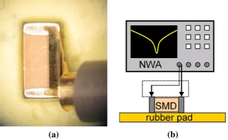
Measurements were realized with a network analyzer equipped with 2000 µm HF probes. The DUT was placed on a rubber mat to avoid the influence of copper pad inductivity and to define a substrate for the measurements. In practical usage the substrate influence has to be considered also as in Lakshminarayanan et al. (2000). The test is demonstrated in Fig. 2. One port S11 scattering parameter (Kurokawa, 1965)
(a) (b)
Fig. 2. (a) Measurement pins of HF probe on 0805 MLCC. (b) Test
setup for impedance curve measurement with NWA.
measurement was carried out and the data was converted to get the impedance curve of the component based on the fol-lowing equation:
Z11=Z0 1+S11 1−S11
(1) Five pieces of the same component were measured. Compo-nents of one series were chosen by size, dielectric material, voltage limit, termination structure.
2.3 Model parameter extraction from measured impedance curves
The impedance curve can be split in three main regions. The capacitor behaves in the first region under series resonance frequency (SRF) as an ideal capacitor. So the impedance is determined by the following equation:
logZ(f <<SRF)
=log
1
2πf C=log 1
2π C−logf (2) At the resonance frequency there is no imaginary part of the impedance value so that the impedance is equal with the re-sistance of the circuit.
logZ(f=SRF)
=R (3)
Over the resonant point the inductive behavior dominates: logZ(f >>SRF)
=log2πf L=log2π L+logf (4)
From Eqs. (2) and (4) follows that a line with a slope of
±logf has to be fitted on the measured data. L and C can be calculated from the y-value at the interception point of the y-axis.
curve. Therefore the equivalent circuit parameters were ex-tracted from each impedance curve and their standard devi-ation was expressed from the average value, on which the curve fitting will be performed later. The standard deviation of the interception parameter of the fitted straight lines dur-ing the parameter extraction was not taken into account since its value was negligible (less than 0,01%). Also the variabil-ity of values around the average is considered to follow ap-proximately a Gaussian distribution. The investigation was performed on the smallest and the largest value for each ca-pacitance range. The standard deviation of the ESC value is small and fits into the capacitance tolerance range given by the manufacturers (±5% for COG and±10% for X7R). Also the equivalent inductance of the components shows an ac-ceptable result, the standard deviation values are below±5% in all cases. Notable differences can be observed only in the case of the ESR values. The measurement of the equivalent series resistance is less accurate for higher capacitance val-ues with this measurement method, as described in Hajdu (2010).
2.4 Curve fitting with non-linear regression
Before performing the nonlinear regression, the appropriate model has to be selected. By taking a look at the shape or tendency of the data points, the main curve category that fits the results can be determined. However, at this step a trade-off has to be made between accuracy and simplicity. After defining the best model a first initial value for the model pa-rameters is required to generate the first curve. To identify the fidelity of the model, the sum-of-squares is calculated. To reach predefined quality, the variables have to be adjusted to make the curve come closer to the data points. The goal is to minimize the sum of squared residuals:
φ(x)= 1 2
m X
i=1
fi2(x)=1
2kF (x)k
2 (5)
WhereF:Rn→Rmandm≥n. Difference of the observed data pointyi and the calculated curve point atxi is denomi-nated asfi whereβis a vector of adjustable parameters.
fi(x)=yi−f (xi;β) (6)
The most commonly used algorithm is the Levenberg-Marquardt method (Mor´e, 1978), which we also used. Some fitting quality indicators were used so that the quality of dif-ferent fittings was comparable. The two indicators we used were adjustedR2andχ2. The coefficient of determination, R2, can be calculated with the following expression with the mean of all observed data,y¯:
R2=1− P
i
(yi−f (xi;β))2
P
i
(yi− ¯y)2
(7)
2 0 0 4 0 0 6 0 0 8 0 0 2 0 0 0 1 0 0
1 0 0 0
2 0 0 4 0 0 6 0 0 8 0 0 2 0 0 0 1 0 0
1 0 0 0
1 1 0
1
1 0
1 1 0
1
1 0
E S C L i n e a r F i t t o E S C
E
S
C
[
p
F
]
n o m . C [ p F ]
0 6 0 3 C 0 G
E S C L i n e a r F i t t o E S C
E
S
C
[
p
F
]
n o m . C [ p F ]
0 8 0 5 C 0 G
0 6 0 3 X 7 R
E S C L i n e a r F i t t o E S C
E
S
C
[
n
F
]
n o m . C [ n F ]
E S C L i n e a r F i t t o E S C
E
S
C
[
n
F
]
n o m . C [ n F ]
0 8 0 5 X 7 R
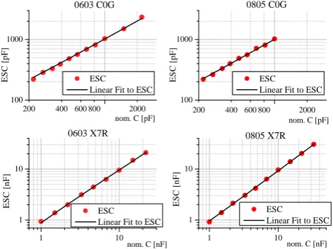
Fig. 3. The extracted ESC values and the results of curve fitting.
R2 can be modified to adjustedR2 to improve informative value with the sample size n and the total number of regres-sors k without the constant term in this form:
adj.R2=1−1−R2 n−1
n−k−1 (8)
The errors can be assumed to have a normal distribution so that a reducedχ2 distribution can be also used to test the quality of fit. The variance σ related to the measurement error foryi is needed for the calculation of the reduced Chi-square.
χred2 =χ
2
ν =
1 ν
X
i
(yi−f (xi;β))2
σ2 (9)
The degrees of freedom (ν) can be calculated asn−k.
3 Fitting results
3.1 Equivalent series capacitance
The nominal capacitance of the measured DUT is dominant at lower frequencies. Therefore the data points resulting from the parameter extraction are expected to be very close to the nominal capacitance value. Figure 3 shows the correspond-ing curve fittcorrespond-ing results for all the four types of capacitors with a linear regression. The outcome meets the previous ex-pectations. The relation between the nominal capacitance of the DUT and the measured ESC values is linear.
The data points are plotted on a logarithmic scaled x- and y-axis, therefore the fitted curves also look linear.
3.2 Equivalent series resistance
2 0 0 4 0 0 6 0 0 8 0 0 2 0 0 0
0
5 0 1 0 0 1 5 0 2 0 0 2 5 0
2 0 0 4 0 0 6 0 0 8 0 0 2 0 0 0
0
5 0 1 0 0 1 5 0 2 0 0 2 5 0
1 1 0
0
5 0 1 0 0 1 5 0 2 0 0 2 5 0 3 0 0 3 5 0 4 0 0
1 1 0
0
5 0 1 0 0 1 5 0 2 0 0 2 5 0 3 0 0 3 5 0 4 0 0
E
S
R
[
m
Ω
]
n o m . C [ p F ]
E
S
R
[
m
Ω
]
n o m . C [ p F ] E S R
H a r r i s F i t A l l o m e t r i c F i t H a r r i s F i t + O f f s e t
E
S
R
[
m
Ω
]
n o m . C [ n F ]
0 8 0 5 C 0 G 0 6 0 3 C 0 G
0 6 0 3 X 7 R
E
S
R
[
m
Ω
]
n o m . C [ n F ]
0 8 0 5 X 7 R
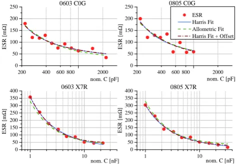
Fig. 4. The extracted ESR values and the results of curve fitting.
of the termination resistances and electrode resistances. A more sophisticated explanation can be found in Coda et al. (1976). Higher capacitance values can be reached with en-larging the overlapping area of the electrode plates, increas-ing the number of the plates, or with decreasincreas-ing the distance between two electrodes. The last has negligible influence on the equivalent resistance; the other two reduce the resistance value. Thus one can expect that the resistance decreases with increasing nominal capacitance value. This expectation is confirmed by the measurement results in Fig. 4.
As there is no information about the internal structure of the capacitor, two standard fitting models were used for curve fitting: Allometric, Harris. They provide good quality and simplicity at the same time. The Harris fit gave a better result. An important aspect has to be taken into consideration. In the case of the two power form functions a reasonable meaning is behind their equations. The so-called Harris fit has a max-imum value that it cannot exceed when the variable goes to zero. On the other hand, it does not have a minimum bound-ary so theoretically a DUT with large capacitance value can have zero ESR. This is obviously impossible. Therefore a modification on the Harris fit was necessary. By introducing a fourth parameter, the resulting function has boundaries for both extreme values. The outputs of the regression analysis for Harris fit with offset are collected in Table 1.
3.3 Equivalent series inductance
The most difficult parasitic component to measure and in-vestigate is the equivalent series inductance. First of all it is performed at frequencies usually above 100 MHz so the imperfections in the measurement setup, the unwanted struc-tural and external effects have extended influence on the ac-curacy. In addition, the value of the ESL in case of chip multilayer ceramic capacitors is quite small mainly due to the SMD packaging, and is usually around 0.5–1.5 nH.
Table 1. Curve-fitting results for the ESR values of the four
differ-ent capacitors with Harris + offset.
0603 C0G 0805 C0G 0603 X7R 0805 X7R
Eq. y=a+(b+cxd)−1
a 15 30 40 20
b −0.02 −5×10⁻⁴ 5×10⁻⁴ 5×10⁻⁴
c 0.01 3×10⁻⁵ 0,002 3×10⁻³
d 0.23 1 1.2 1
Red.χ2 230.9 585.3 78.2 128.7
Adj.R2 0.85 0.73 0.99 0.98
The investigation of the measured results is also more complicated. To find out the source of ESL, again the struc-ture of the chip multilayer capacitor shown in Fig. 1 should be inspected. The electrodes can be considered as flat metal-lic plates, whose thickness is negligible compared to the other two dimensions. Each elemental capacitor is in series with itself not only its own self-inductance, but also the mu-tual inductance of all the other plates, the magnitude of which will diminish with the plate spacing. As these spacings are generally small, these mutuals will approach, though never exceed, the self-inductance of any one plate. The inductance in series with each elemental capacitor will therefore not ex-ceed nL. With n capacitors with L inductance in parallel, and since these can now be considered fully decoupled, the effective inductance of the whole capacitor will be the in-ductance of any one of them divided by n. This means that in case of the two extreme conditions, the resultant induc-tance does not change as the number of layers increases if the spacing between them is small enough. Or it decreases by 1/nif the electrodes are far from each other. Here the in-fluence of mutual inductances between the terminals and the end of the opposite electrodes or between two parallel but not overlapping plates are neglected, since they are a lot smaller in value compared to those between the overlap region of the plates. Also the inductance of the terminals themselves has to be taken into account. To simplify the calculation, they can be considered to be constant for the investigated series of capacitances since the geometry of the SMD packaging does not differ to a great extent. As a consequence of the previously mentioned relationships, the ESL value of a chip multilayer ceramic capacitor is expected to decrease as the nominal capacitance increases, but because of the many in-fluential parameters (plate geometry and number of layers) the correlation might be more complicated.
The previous expectations seem to be valid in most of the cases if we take a look at the fitted curves in Fig. 5 for all the four different capacitor types.
2 0 0 4 0 0 6 0 0 8 0 0 2 0 0 0 8 0 0
8 5 0 9 0 0 9 5 0 1 0 0 0 1 0 5 0 1 1 0 0
2 0 0 4 0 0 6 0 0 8 0 0 2 0 0 0 8 0 0
8 5 0 9 0 0 9 5 0 1 0 0 0 1 0 5 0 1 1 0 0
1 1 0
7 0 0 7 5 0 8 0 0 8 5 0 9 0 0 9 5 0 1 0 0 0 1 0 5 0 1 1 0 0
1 1 0
7 0 0 7 5 0 8 0 0 8 5 0 9 0 0 9 5 0 1 0 0 0 1 0 5 0 1 1 0 0
E S L E x p o n e n t i a l F i t
E
S
L
[
p
H
]
n o m . C [ p F ]
0 6 0 3 C 0 G
E S L L i n e a r F i t
E
S
L
[
p
H
]
n o m . C [ p F ]
0 8 0 5 C 0 G
E S L E x p . F i t ( 1 n F - 4 , 7 n F ) E x p . F i t ( 6 , 8 n F - m a x )
E
S
L
[
p
H
]
n o m . C [ n F ]
0 6 0 3 X 7 R
E
S
L
[
p
H
]
n o m . C [ n F ]
0 8 0 5 X 7 R
Fig. 5. The extracted ESL values and the results of curve fitting.
(a) (b)
Fig. 6. Cross section view of 0805 X7R capacitances with
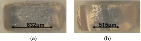
(a) 4.7 nF and (b) 6.8 nF.
4.7 nF and 6.8 nF. The increased capacitance value is reached with an increased number of plates but their dimensions are lesser. This is depicted in Fig. 6.
Unfortunately no such behavior could be observed regard-ing the components with C0G type dielectric, although in the case of the 0603 sized DUT the data points are still not ran-domly scattered, so here the distribution was approximated also by an exponential function. For the 0805 sized C0G type capacitor, a reasonable fitting function could not be found, so a simple linear one was used.
4 Implementation of the model
To test the previously expressed equations of the scalable models they have to be implemented in a circuit simulator. The implementation was realized as a subcircuit in Saber. A little trick was needed because the compiler of Saber does not understand every mathematical operation. Therefore the implemented equations look a bit more complex, because the power operation was substituted by the combination of expo-nential and logarithm functions. The step in the ESL curve of X7R capacitors between 4.7 nF and 6.8 nF, which has been explained in Sect. 3.3, was realized by the use of the int com-mand, which rounds the operand to the nearest integers to-wards minus infinity. Realization for the 0805 X7R capacitor (right bottom corner in Figs. 3–5) is in Fig. 7, where C nom is the nominalvalue of the capacitor in nF.
c.c1=1e-9*(0.0391+0.925*{C_nom})
l.l1=1e-12*((835.3-(int(({C_nom}/(6.8+{C_nom}))+0.5)*53.8))+... (17111.4-(int(({C_nom}/(6.8+{C_nom}))+0.5)*16411.6))*... exp((-4.74+(int(({C_nom}/(6.8+{C_nom}))+0.5)*4.57))*{C_nom}))
rnom.r1=1e-3*(15+1/(5e-4+2.97e-3*exp(0.96*ln({C_nom}))))
Fig. 7. Subciruit realization of the scalable model for one 0803 size
X7R capacitor.
Frequency [Hz]
1meg 10meg 100meg 1g
Impedance
Mag.
[Ohm]
10.0m 1.0 100.0 10.0k
Static
Scalable
Fig. 8. Comparison of scalable and static model impedance
magni-tude for 0805 X7R capacitance series.
The scalable models were compared with the static models to validate them. The goal was to show that they are almost as good a quality as static models are. The comparison of the model shown in Fig. 7, is in Fig. 8.
The difference between the simulation and the measure-ment is quite small in the case of this series, but to have a better overview, the accuracy of each equivalent circuit pa-rameter has to be tested. Therefore results of those capaci-tances were collected where the difference between the mea-sured value and the fitted curve was the biggest. In this way the maximal margin can be determined and so the worst case situation can be investigated. The results are collected in Ta-ble 2. The accuracy is very high in all cases except in case the of the ESR. The measurement uncertainty of the resis-tance value also influences this result (see Sect. 3.2). This value is responsible for the amplitude in the spectrum which is measured usually in dB. For that reason this deviation is also acceptable for EMC purposes.
5 Possible usage in EMC
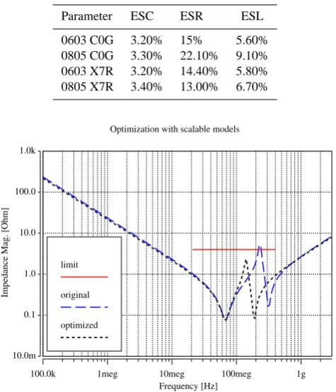
Table 2. Maximal modelling failures.
Parameter ESC ESR ESL
0603 C0G 3.20% 15% 5.60%
0805 C0G 3.30% 22.10% 9.10% 0603 X7R 3.20% 14.40% 5.80% 0805 X7R 3.40% 13.00% 6.70%
Optimization with scalable models
Impedance
Mag.
[Ohm]
10.0m 0.1 1.0 10.0 100.0 1.0k
Frequency [Hz]
100.0k 1meg 10meg 100meg 1g
limit
original
optimized
Fig. 9. Optimization of an input filter of two parallel SMD
capaci-tors.
One typical task is the parameter optimization for input fil-ters. In Fig. 9 is an example of two parallel 0603 size scal-able capacitor models with X7R (1–22 nF) and C0G (220– 2200 pF) dielectric for input filter optimization.
The advantageous behaviour of the scalable models is that they are easily extendable. With new functions within the subcircuit, more optimization goals can be defined simulta-neously e.g. thermal, cost. The thermal or cost functions can be determined with the same method as the parasitics above.
6 Conclusions
Scalable models can be used in simulations, when a rapid op-timization is desired. They reduce the number of parameters
to be changed and therefore save computing capacity. Val-idation of the models must be proved with statistical mea-surement data if possible. A very good model approxima-tionwith interpolation is possible for unknown components of one model series, which is presented with only few known components. This can be considered as a time-saving possi-bility for fast modelling. If a sufficient level of maturity is achieved in such models, these models can provide as good a quality as static models do for many component types. Good scalable modelling can be achieved with components in se-ries that have little scattering regarding nominal value and parasitic values. SMD components are suitable for such a modelling.
References
CISPR SC/D: CISPR 25 Vehicles, boats and internal combustion engines – Radio disturbance characteristics – Limits and methods of measurement for the protection of on-board receivers, Stan-dard, IEC, 2008.
Coda, N. and Selvaggi, J. A.: Design Considerations for High-Frequency Ceramic Chip Capacitors, IEEE Trans on Parts, Hy-brids, Packag, 12(3), 206–212, 1976.
Cojocaru, V., Markell, D., Capwell, J., Weller, T., and Dunleavy, L.: Accurate Simulation of RF Designs Requires Consistent Model-ing Techniques, High Frequency Electronics, 1(2), 46–51, 2002. Hajdu, A.: High-Frequency Characterization and Modeling of
Elec-tronic Components, Diploma Thesis, 2010.
Kurokawa, K.: Power Waves and the Scattering Matrix, IEEE Trans. on MTT, MTT-13(2), 194–202, 1965.
Lakshminarayanan, B., Gordon Jr., H. C., and Weller, T. M.: A Substrate-Dependent CAD Model for Ceramic Multilayer Ca-pacitors, IEEE Trans. on Microwave Theory and Techniques, 48(10), 1687–1693, 2000.
Leibinger, A.: Automatisierungsmglichkeiten der EMV Opti-mierung in der Netzwerksimulation, AmE 2010 Conf., Dort-mund, 2010.
Mor´e, J. J.: The Levenberg-Marquardt algorithm: Implementation and theory In Numerical Analysis, edited by: Watson, G. A., Lecture Notes Math., 630, 105–116, Springer, 1978.
Seber, G. A. F. and Wild, C. J.: Nonlinear Regression, John Wiley & Sons, Canada, 1989.