M. Nawito1, H. Richter1, A. Stett2, and J. N. Burghartz1 1Institut für Mikroelektronik Stuttgart, Stuttgart, Germany
2NMI Naturwissenschaftliches und Medizinisches Institut an der Universität Tübingen, Reutlingen, Germany
Correspondence to: M. Nawito ([email protected])
Received: 15 December 2014 – Revised: 9 April 2015 – Accepted: 15 July 2015 – Published: 3 November 2015
Abstract. In this work an Application Specific Integrated Circuit (ASIC) for an implantable electrochemical biosensor system (SMART implant, Stett et al., 2014) is presented. The ASIC drives the measurement electrodes and performs am-perometric measurements for determining the oxygen con-centration, potentiometric measurements for evaluating the pH-level as well as temperature measurements. A 10-bit pipeline analog to digital (ADC) is used to digitize the ac-quired analog samples and is implemented as a single stage to reduce power consumption and chip area. For pH measure-ments, an offset subtraction technique is employed to raise the resolution to 12-bits. Charge integration is utilized for oxygen and temperature measurements with the capability to cover current ranges between 30 nA and 1 µA. In order to achieve good performance over a wide range of supply and process variations, internal reference voltages are generated from a programmable band-gap regulated circuit and bias-ing currents are supplied from a wide-range bootstrap cur-rent reference. To accommodate the limited available elec-trical power, all components are designed for low power op-eration. Also a sequential operation approach is applied, in which essential circuit building blocks are time multiplexed between different measurement types. All measurement se-quences and parameters are programmable and can be ad-justed for different tissues and media. The chip communi-cates with external unites through a full duplex two-wire Se-rial Peripheral Interface (SPI), which receives operational in-structions and at the same time outputs the internally stored measurement data. The circuit has been fabricated in a stan-dard 0.5-µm CMOS process and operates on a supply as low as 2.7 V. Measurement results show good performance and agree with circuit simulation. It consumes a maximum of 500 µA DC current and is clocked between 500 kHz and
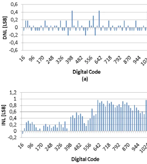
4 MHz according to the measurement parameters. Measure-ment results of the on-chip ADC show a Differential Non Linearity (DNL) lower than 0.5 LSB, an Integral Non Lin-earity (INL) lower than 1 LSB and a Figure of Merit (FOM) of 6 pJ/conversion.
1 Introduction
An integral part of all types of active implantable medical de-vices, such as cochlear and brain implants, is the electronic module. For monitoring of neuronal and metabolic activity a readout chip has to be implemented, which controls the data acquisition and management. In case of biosensor appli-cations like subcutaneous metabolic monitoring, the electro-chemical detection of ions, oxygen and pH requires a precise setting and measurement of voltage and currents at the metal-lic microelectrodes (Kubon et al., 2010; Jafari et al., 2014). For applications where large batteries and cabling is not suit-able, stringent requirements on the readout chip in terms of size and energy efficiency are placed.
Figure 1. (a) Block diagram of the SMART Implant system highlighting readout ASIC, (b) photograph of actual implant and housing structure.
presented. The aim here is not to go through all the numer-ous analog and digital circuit blocks individually, but rather to give a description of the chip’s functionality and struc-ture, highlighting issues of energy efficiency, programmabil-ity and reliabilprogrammabil-ity of operation, in addition to the design tech-niques employed to approach these aspects.
2 Measurement sequence
The ROIC drives the measurement electrodes and performs amperometric measurements for determining the oxygen concentration, potentiometric measurements for evaluating the pH-level as well as temperature measurements. In order to increase the data integrity of the measurement process, a sequential approach has been adopted, hence avoiding any disturbance that might occur due to simultaneous sampling and processing of different signals. To further improve the quality of the acquired data, a number of up to 128 “single measurements” are preformed and then averaged in order to obtain a measurement sample. This way random spikes or er-ratic data points are eliminated, which are generated due the fluctuating nature of the chemical reaction taking place be-tween the electrode surface and the connected tissue (Lind-ner et al., 1986). The measurement samples form a “mea-surement sequence”, which would eventually settle to a final value. The number of samples and the final value are deter-mined by the external microcontroller according to the crite-ria set by the International Union of Pure and Applied Chem-istry (IUPAC; Lindner et al., 1986). The aforementioned con-cept is illustrated in Fig. 2. As shown, it is a requirement for single measurements, whether they are of temperature, pH or O2type, to be performed at least every 128 µs, but the time scale for a final value to be reached is in the order of sec-onds. The chip performs a complete measurement sequence each 15 min. Figure 2 also emphasizes the necessity for an energy efficient design since the ROIC is supposed to remain operational inside the battery operated implant for duration up to 4 weeks.
Figure 2. Measurement cycle as performed by the ROIC.
mea-set, the input channels and current range are set and the bandgap circuit is either turned on or off.
surement conditions. For this reason the calibration and pre-setting of the ROIC is imperative to allow for meaningful in-terpretation of the results. For example when performing O2 measurements, the settling time required for the electrodes to start producing measurable currents differs from one material to another, hence the settling time is calibrated according to the tissue to be characterized.
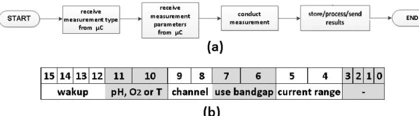
Figure 3a shows the implemented flow chart of the ROIC. The chip receives a 16 bit operational code or opcode, where the first 4 bits constitute the instruction to be carried out (measure, calibrate, sleep etc.) and the relevant parameters are packed in the remaining 12 bits. As an example, Fig. 3b illustrates the structure of the wakeup command and the parameters passed to the chip during wakeup process. As seen during wakeup the measurement type and measurement channels are chosen, in addition to the setting of the current measurement range for O2 and temperature measurements. Also for testing and calibration purposes, reference voltages of the ADC could be either controlled by a bandgap circuit or generated directly from a simple resistive divider, hence the option “use bandgap” is available during wakeup.
3 ASIC structure
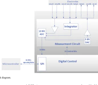
To implement the functions described in the previous section, the ASIC has been divided into digital and analog sections, as shown in Fig. 4. For both O2and pH measurements, two measurement channels have been implemented respectively.
3.1 Digital circuits
For communication, a full duplex Serial Peripheral Interface (SPI) is implemented allowing the chip to simultaneously re-ceive the 16 bit opcode from the external microcontroller and to send measurement results as a 16 bit output data word. The digital controller interprets the received opcodes and ac-tivates the analog circuitry which drives the external elec-trodes connected to the tissue and carry out the actual mea-surement. In case of a data transmission error or a faulty op-code, the chip sends an interrupt signal to request a resending
of the instructions. To realize an energy efficient operation, all measurements are conducted with only the needed analog blocks turned on. For example since the charge integrator, as will be discussed shortly, is only required for amperometric sensing, it is turned off during potentiometric measurements. In the case of idle times where the chip is not measuring, all components are turned off except for the SPI interface which continues to listen for incoming instructions.
3.2 ADC
A central component of the readout path is a 10 bit cyclic ADC based on the pipelined principle, which converts the measured signal and sends it to the digital core for process-ing and storage. The ADC is designed to convert input volt-ages between 0.5 and 2.5 V with a LSB of 1.96 mV. The pipelined architecture has been chosen due to its relatively simple circuitry, reliable operation and capability of achiev-ing the required 10 bit resolution needed for temperature and O2measurements. A typical structure for such an ADC would consist of 9 stages in series, each producing 1.5 bits, and some form of digital correction. However, the large chip area occupied by such an arrangement in addition to its high power consumption would be unacceptable for this applica-tion, which necessitated a modified design. Figure 5 shows the implemented ADC which consists of a single 1.5 bit stage followed by a sample and hold circuit. The input analog sig-nal is converted by the sub ADC, the residue is sampled by the sample and hold stage and then same circuit is reused again until the 10 bit word is produced. In other words in-stead of converting the analog input through 9 stages, a sin-gle stages is reused 9 times, reducing the area and power con-sumption by almost an order of magnitude.
3.3 pH measurement
gen-Figure 4. ROIC block diagram.
Figure 5. ADC circuit with special pH mode switches and capacitors.
erated by the measurement electrodes, which corresponds to the measured pH value and lays between 0.7 and 2.3 V, is first converted to a 10 bit “coarse” word, then according to the conversion result, a known offset generated by the on-chip 5-bit Digital to Analog Converter (DAC) (shown in Fig. 4) is subtracted from the original input. The difference is mul-tiplied by 4 and converted to a 10 bit “fine” word. Summing the value of the offset and the fine results gives the final value with the required 12 bit resolution. To realize the aforemen-tioned process, switches Sph1 and Sph2 , in addition to ca-pacitors with the valuesCand 3Care added as a new
modi-fication to the circuit, as highlighted in Fig. 5, since they are specifically used to carry out the offset subtraction and differ-ence multiplication. Specifically, in the first phase of the pH mode operation, switches are clocked so that the multiplying DAC connecting these elements with is connected as shown in Fig. 6a, where in that case the total charge of the system is given by
and the total charge is given by
Qphase2=Vout×C+Voffset×4C. (2) Since Qphase1 equals Qphase2 the final output voltage is given by
Vout=4(Vin−Voffset) . (3)
3.4 O2and temperature measurement
In the case of O2 and temperature measurement, the mea-sured analog signals are currents, where for the former a three electrode measurement setup is implemented and cur-rent flowing between the working electrode and the counter electrode is of interest (Kubon et al., 2010). For temperature measurements, an external Schottky diode is reversed biased and used as a transducer, where the reverse current is a mea-sure of the temperature and the sensitivity of the sensor is controlled by the reverse bias voltage. The reverse voltage is also produced by the internal DAC and is one of the parame-ters to be set by the user.
To convert currents into voltages, a necessary step given that the ADC operates on voltage inputs, the charge inte-grator shown in Fig. 6. is implemented. Following the basic equation of charge integration which states that
Vout= Iin×t
C , (4)
whereVoutis the output voltage,Iinis the input current,t is the integration time andCis the integration capacitance, it is clear that by adjustingtandC, various current ranges can be measured. For this reason, different integration capacitances are added in parallel, as illustrated in Fig. 7. Furthermore, the integration time can be set as an input parameter, allowing the implemented integrator to cover current ranges between 30 nA and 1 µA with a 10 bit resolution.
4 Fabrication
The design has been implemented using IMS GATE FOREST® 0.5 µm, 2 Metal CMOS technology
Figure 7. Programmable charge integrator.
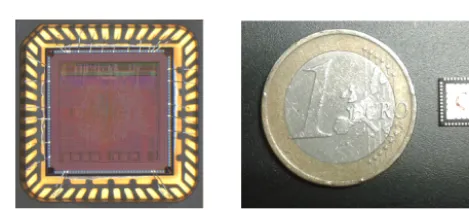
Figure 8. (a) Photograph of fabricated chip in housing, (b) size comparison between final chip and a coin.
(http://www.ims-chips.de/content/pdftext/White_paper_ MS_Array_09_11.pdf). This sea of transistors technology offers transistors and passive circuit elements implemented in a certain number of fixed dimensions. The digital and ana-log circuits are then realized by connecting these elements with metal wires creating semi custom designs. A major advantage of this approach is that the devices are very well characterized and modeled, enhancing the process yield and the reliability of the ASIC.
In Fig. 8a, a photograph of the fabricated ASIC bonded inside a QFN48 housing is shown, where Fig. 8b shows a size comparison between the final sealed housing to be used in the actual implant and a coin.
5 Measurement results
Figure 9. (a) Measured ADC DNL, (b) measured ADC INL.
Table 1. Performance parameters of the ROIC.
Technology 0.5 µm, 2M CMOS, see of gates
Supply 2.7–3.3 V
Temperature 20–80◦C
Max. total DC current ∼500 µA at 3.3 V, 80◦C Min. total DC current ∼250 µA at 2.7 V, 20◦C Nominal operating frequency 500 kHz
Max. operating frequency 4 MHz Number of analog devices 432 Number of digital gates 1185 (NAND equiv.)
The chip operates at supply voltages between 2.7 and 3.3 V and at temperatures between 20 and 80◦C, where the temperature measurement circuits have been optimized for the range between 20 and 43◦C with an accuracy of 0.1◦C. The maximum total DC current that all circuits could consume is about 500 µA nevertheless, this value is never reached since that would require all digital and analog build-ing blocks to be turned on at the same time. As mentioned before, this case is avoided by activating the relevant compo-nents for a certain measurement type only. In order to reduce dynamic power consumption and at the same time fulfill-ing the requirement of obtainfulfill-ing a sfulfill-ingle measurement point every 128 µs given the cyclic nature of the ADC, a nomi-nal operating frequency of 500 kHz is chosen. However, the chip can function reliably at a maximum frequency of up to
process should be the consideration of energy requirements and the fulfilment of flexible operation during all phases of the design. Efficient scheduling of the measurement se-quence, implementing an elaborate set of operations and the time multiplexing of internal components, in addition to the optimization of power consumption on the circuit level are all important methods in their own right, but yield the most interesting results when employed in combination.
Acknowledgements. This work was funded by the German Federal Ministry of Education and Research, BMBF as part of the MicroTEC Südwest Cluster project SMART Implant, grant no. 16SV5979K, 16SV5980 and 16SV5982-86. The authors would also like to sincerely thank all members and partners of the SMARTImplant consortium. Without their valuable efforts, this work would not have been possible.
Edited by: D. Killat
Reviewed by: two anonymous referees
References
Jafari, H. M., Abdelhalim, K., Soleymani, L., Sargent, E. H., Kel-ley, S. O., and Genov, R.: Nanostructured CMOS Wireless Ultra-Wideband Label-Free PCR-Free DNA Analysis SoC, IEEE Jour-nal of Solid-State Circuits, 49, 1223–1241, 2014.
Kubon, M., Moschallski, M., Link, G., Ensslen, T., Werner, S., Burkhardt, C., Nisch, W., Scholz, B., Schlosshauer, B., Urban, G., and Stelzle, M.: A Microsensor System to Probe Physiolog-ical Environments and Tissue Response, IEEE Conference on Sensors, Kona, Hawaii, 1–4 November 2010, 2607–2611, 2010. Lindner, E., Toth, K., and Pungor, E.: Definition and determination of response time of ion selective electrodes, Pure Appl. Chem, 58, 469–479, 1986.