University of New Orleans University of New Orleans
ScholarWorks@UNO
ScholarWorks@UNO
University of New Orleans Theses and
Dissertations Dissertations and Theses
12-15-2007
Magnetic and Transport Properties of Oxide Thin Films
Magnetic and Transport Properties of Oxide Thin Films
Yuanjia Hong
University of New Orleans
Follow this and additional works at: https://scholarworks.uno.edu/td
Recommended Citation Recommended Citation
Hong, Yuanjia, "Magnetic and Transport Properties of Oxide Thin Films" (2007). University of New Orleans Theses and Dissertations. 615.
https://scholarworks.uno.edu/td/615
Magnetic and Transport Properties of Oxide Thin Films
A Dissertation
Submitted to the Graduate Faculty of the University of New Orleans in partial fulfillment of the requirements for the degree of
Doctor of Philosophy in
Engineering and Applied Science
by
Yuanjia Hong
M.S. Changchun Institute of Optic and Fine Mechanics, ChangChun, P.R.China, 2000
ACKNOWLEDGEMENTS
This dissertation was funded in part by Sharp Laboratories of America and by Louisiana
Board of Regents Support Fund Grant No. LEQSF(2004-07)-RD-B-12.
I would like to say first and foremost what an honor to receive the guidance of Dr. Jinke
Tang. He provided me the opportunity to come to the United States to work on my degree
through the offer of an assistantship to work in his research group. Through the years, he has
shown me keen academic insight, and great patience, and has shared his extensive acknowledge
both in and beyond science. His wise guidance has helped shape my career and my life.
It has been an enjoyable learning experience to work with my Committee members Dr.
Carl Ventrice, Dr. Rasheed M. A. Azzam, Dr. Ashok Puri and Dr. Kevin Stokes. I am sincerely
grateful for all their time and assistance. I also would like to thank Dr. Leszek Malkinski for
serving on my general exam committee.
I would like to thank the following for their experimental expertise, and the use of their
equipment in my research: Dr Leonard Spinu, Dr. John B. Wiley, and Dr. Weilei Zhou. I also
learned considerably from Dr. Wendong Wang, Dr. Zhenjun Wang. I would like to thank Dr.
Hongguo Zhang, Dr. Minghui Yu, Dr. Gabriel Caruntu, Mr. Cosmin Radu, Mr. Jiajun Chen and
Mr. Renhai Long for their assistance in my experimental work.
I would like to thank Ms. Pat Robbert for sharing her experience and countless interesting
and stimulating discussions.
Thanks to Dr. C. Greg Seab, Dr. George Ioup and Dr. Juliette Ioup, who took the time to
help and guide me in the PhD program, and were supportive over the years. Thank you to Mr.
challenges of keeping the department running smoothly, including all the extra help involved
with an international student.
I have more than usual thankfulness that I would like to express for assistance given
during the difficult period after Hurricane Katrina.
To Tao Fang, Chairman of the LSU Chinese Student and Scholar Association, along with
his wife Tao Yang, for the best care to student evacuees from new Orleans.
To Dr. Jeffery M. Gillespic and his wife Ms. Michelle Gillespie, who generously shared
their sweet home with me and other evacuees after Katrina.
To Dashun Xue, Rong Zheng, and other classmates for the generosity to a guest student at
LSU after Hurricane Katrina
To Ms. Pat Robbert and Dr. Stanley Goldberg who provided me a home while I was
awating a FEMA trailer.
Thank you to the many friends I have met at UNO.
Thank you to Dr. Ronald C. Miller and Dr. Weldon Wilson for making time in their busy
schedules to help me polish my English.
Thank you to Dr. Stephen Michael Rodrigue, who always brings inspiration and
encouragement to me; he helped me through many difficulties along the way of pursuing my
PhD. His belief in me has allowed me to increase my self-confidence.
Thank you to my dearest family, Yachen Yuan and Guangyan Hong, the foundation of
my life, love, sacrifice and dedication and I am eternally grateful for all of your love and
ABSTRACT...III
CHAPTER 1 ...1
INTRODUCTION ...1
1.1 Spintronics ...1
1.2 Spintronics in Semiconductors --- Spin Injection...3
1.3 Half Metals...6
1.4 Magnetic Semiconductors...7
1.5 Oxide-diluted magnetic semiconductors...8
CHAPTER 2 ...13
EXPERIMENTAL TECHNIQUES...13
2.1 Introduction to Pulsed Laser Deposition...13
2.2 Deposition Principles and Deposition System...15
2.2.1 Lasers ...16
2.2.2 Deposition Systems...18
2.2.3 High Vacuum System ...20
2.3 Film Growth by Pulsed Laser Deposition...21
2.3.1 Substrate Materials for O-DMS Films...21
2.4 Thin Film Characterization ...22
2.4.1 X-Ray Diffraction ...22
2.4.2 Physical Properties Measurement System (PPMS) ...23
2.4.3 Superconducting Quantum Interference Device (SQUID) ...24
2.4.4 Transmission Electron Microscope (TEM) ...25
CHAPTER 3 ...27
THE STRUCTURE AND MAGNETIC PROPERTIES OF TIN DIOXIDE THIN FILMS ...27
3.2 Experiments ...29
3.3 Results and Discussion ...30
3.4 Conclusions...37
CHAPTER 4 ...39
ROLE OF DEFECTS IN TUNING FERROMAGNETISM IN DILUTED MAGNETIC OXIDE THIN FILMS ...39
4.1 Introduction...39
4.2 Experiment...40
4.3 Experimental Results and Didcussion ...41
4.4 Conclusions...45
CHAPTER 5 ...47
STRUCTURE AND MAGNETIC PROPERTIES OF PURE AND GADOLINIUM-DOPED HAFINIUM DIOXIDE THIN FILMS...47
5.1 Introduction...47
5.2 Pure HfO2 Thin Films ...48
5.2.1 Experiments ...48
5.2.2 Structure Analysis...49
5.2.3 Magnetic Properties ...52
5.2.4 Signals From The Substrates ...54
5.3 Gd Doped HfO2 Thin Film ...60
5.4 Defects Hypnosis ...64
5.4.1 HfO2 Thin Film ...64
5.4.2 HfO2 Powder...66
5.5 Conclusion ...69
REFERENCES ...71
Vita...71
ABSTRACT
My dissertation research focuses on the investigation of the transport and magnetic
properties of transition metal and rare earth doped oxides, particularly SnO2 and HfO2 thin films.
Cr-and Fe-doped SnO2 films were deposited on Al2O3 substrates bypulsed-laser deposition.
X-ray-diffraction patterns (XRD) show that the films have rutile structure and grow epitaxially
along the (101) plane. The diffraction peaks of Cr-doped samples exhibit a systematic shift
toward higherangles with increasing Cr concentration. This indicates that Cr dissolvesin SnO2.
On the other hand, there is no obviousshift of the diffraction peaks of the Fe-doped samples. The
magnetization curves indicate that the Cr-doped SnO2 films are paramagneticat 300 and 5 K.
The Fe-doped SnO2 samples exhibit ferromagneticbehaviour at 300 and 5 K. Zero-field-cooled
and field-cooled curves indicatesuper paramagnetic behavior above the blocking temperature of
100 K, suggesting thatit is possible that there are ferromagnetic particles in theFe-doped films.
It was found that a Sn0.98Cr0.02O2 film became ferromagnetic at room temperature after
annealing in H2. We have calculated the activation energy and found it decreasing with the
annealing, which is explained by the increased oxygen vacancies/defects due to the H2 treatment
of the films. The ferromagnetism may be associated with the presence of oxygen vacancies
although AMR was not observed in the samples.
PureHfO2 and Gd-doped HfO2 thin films have been grown ondifferent single crystal
substrates by pulsedlaser deposition. XRD patterns show that the pureHfO2 thin films are of
single monoclinic phase. Gd-doped HfO2films have the same XRD patterns except that their
Transmission electron microscopy images show acolumnar growth of the films. Very weak
ferromagnetism is observedin pure and Gd-doped HfO2 films on different substrates at300 and
5 K, which is attributed to either impure targetmaterials or signals from the substrates. The
magnetic properties donot change significantly with post deposition annealing of the HfO2 films.
Keywords
SnO2, HfO2, pulsed laser deposition, thin film, epitaxial growth, magnetic thin films,
CHAPTER 1
INTRODUCTION
1.1 Spintronics
Traditional silicon chips in computers and other electronic devices control the flow of
electrical current by modifying the positive or negative charge of different parts of each tiny
circuit. Spintronics is "Spin-based electronics". The idea is to use the electron's spin, as well as
its charge in the devices. Spins can exist in one of two states-- “up” or “down”, and this quality
can be exploited to build smaller (potentially on atomic scale) binary devices that are
non-volatile, faster, and more robust and use less power than charge-current-based devices.
Furthermore, because of its quantum nature, electron spin may exist not only in the “up” or
“down” state but also in many intermediate states depending on the energy of the system. All
these qualities hold the potential for what is in effect highly parallel commutating, which is the
basis for the quantum computers.1
Spintronics is not science fiction; it is already used in modern computers. The most
successful spintronic device up-to-date is the GMR spin valve. This device utilizes a layered
structure of thin films of magnetic materials, which change its electrical resistance depending on
applied magnetic field direction. In a spin valve, as shown in Fig. 1.1, one of the ferromagnetic
layers is "pinned"(top layer in Fig. 1.1), so its magnetization direction remains fixed, the other
ferromagnetic layer is "free" to change depend on the applied magnetic field. When the applied
direction, the electrical resistance of the device reaches its lower level. On the other hand, when
the applied external field causes the free layer magnetization vector to rotate in a direction
antiparallel to the pinned layer magnetization vector, the electrical resistance of the device reach
its higher level due to spin dependent scattering.
Fig. 1.1 Schematic diagram of spin valve.
GMR stands for giant magnetoresistance, it was independently discovered in 1988 in
Fe/Cr/Fe trilayers by a research team led by Peter Grünberg of the Jülich Research Centre, who
owns the patent2, and in Fe/Cr multilayer by the group of Albert Fert of the University of
Paris-Sud, who first saw the large effect in multilayer that led to its naming, and first correctly
explained the underlying physics. The discovery of GMR is considered as the birth of spintronics
and has earned both Grünberg and Fert the 2007 Nobel prize3. The primary advantage of GMR
heads is greater sensitivity to magnetic fields from the disk. This increased sensitivity makes it
possible to detect smaller recorded bits and to read these bits at higher data rates. Larger signals
densities beyond 11.6 Gbits/in².4 The hard drive read heads in the current generation of
computer hard drives utilize structures that consist of two layers of metallic ferromagnets (such
as., Fe-Ni alloy) separated by a thin spacer layer (in the order of nm) of normal metal (such as Cr
or Cu)5. The flow of current across the spacer layer is facilitated or inhibited depending on
whether the magnetic moments of the two ferromagnets layers are parallel or anti-parallel to each
other. Devices have been demonstrated with GMR ratios (i.e. the magnitude of the change,
(Antiparallel Resistance - Parallel Resistance) / Parallel Resistance) as high as 60-70%.
Another success story of spintronics is room temperature tunnelling magnetoresistance
(TMR), which was discovered in 1995 by Moodera et al6. When the normal metal layer in a spin
valve is replaced by a thin insulator layer, electrons’ tunnelling probability depends on the
relative orientations of the two magnetic electrodes, and a very large TMR is achieved in such
magnetic tunnel junctions). The discoveries help build up the foundation for a new generation of
magnetic random access memory (MRAM)
1.2 Spintronics in Semiconductors --- Spin Injection
A modern computer chip contains many millions of tiny transistors; each acting as a tiny
switch where a small current is used to control the flow of a larger current. Central to the success
of modern electronics is the transistor. A transistor is a switch that controls the flow of electrical
The spin transistor utilizes both the spin and electronic characteristics of a conventional
semiconductor transistor in combination with a carrier (current) flow controlled by magnetic
moment to maximize gain.
Figure 1.2 below are schematic diagram of a spin transistor. Room temperature
ferromagnetic semiconductor material will replace the n-type semiconductor both in the source
(injector) and drain (collector) area. A spin injector can be occupied by spin polarized charge
carriers with selected magnetic moment. In the collecting (drain) region, the electronic spins can
be determined via application of an electric field, with the initial voltage applied on both the gate
and the drain area, the current flow can be manipulated by the passing through or not via the
magnetic barrier7.
Unlike a normal electrical circuit that requires a continuous supply of power, these spin
states are stable without necessarily requiring the application of an electric current, thus a spin
transistor remains in the same magnetic state even when power is removed, which may lead to
creating cost-effective non-volatile solid state storage device. It is one of the technologies being
(a) (b)
Fig. 1.2 Schematic of a spin transistor.
The challenges to using spintronics for logic operations are so daunting. Not the least
among them is finding the right material to build practical circuits. Remarkable progress has
been made in recent years on all fronts. In particular, the plausibility of semiconductor
spintronics has been bolstered by recent advances such as demonstration of coherent spin
transport over macroscopic distances in a variety of semiconductors8 and the discovery of a host
of magnetic semiconductors9. However, there still have some challenge; such as (1) how to
make spin injection from the ferromagnetic into the semiconductor as efficiently as possible,
because the electrical current in the semiconductor injected from a ferromagnetic metal is
consistently found to have minimum spin polarization. (2) What will be the mechanism of spin
Many approaches are being attempted to address these problems. From materials
synthesis point of view, for example, the use of magnetic semiconductors with crystalline and
electrical properties compatible with conventional semiconductors and with close to 100% spin
polarization is encouraging. A promising group of materials are ferromagnetic oxides and
related compounds, which are predicted to have 100%, spin polarization and referred to as
“half-metals”.10 Interface engineering to generate non-diffusive transport such as tunnelling across the
interface is another approach to enhance the spin injection into a semiconductor.
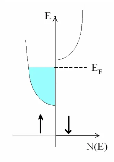
1.3 Half Metals
The conduction of the spintronic devices, either spin-valve or first generation MRAM,
depends firmly on the spin polarization of the ferromagnetic layers, and normally it is 40% in
alloys such as Fe, Co, and Ni. Half metals11 are ferromagnets with an unusual band structure and
have only one type of conduction electron states at the Fermi level (EF) shown in Fig. 1.3.
Half-metals are 100% spin polarized based on theoretical calculation. Well-known half-Half-metals
include Fe3O4, CrO2, Heusler alloys, and perovskite La0.7Sr0.3MnO3.
1.4 Magnetic Semiconductors
Magnetic semiconductors are materials that exhibit both ferromagnetism and
semiconductor properties. Whereas traditional electronics device are based on control of charge
carriers (n-type or p-type), magnetic semiconductors would, in addition, allow control of spin
states (up or down). What is interesting is that they would also provide 100% carrier spin
polarization (thus behave much like a half-metal) in principle, which is important for spintronic
applications, e.g., spin injection in spin FET as mentioned earlier.
An important class of magnetic semiconductor is dilute magnetic semiconductors (DMS),
which are semiconductors doped with transition metals, i.e. electronically active elements. A
few established III-V compound semiconductors such as GaAs become ferromagnetic when
doped with 3-8% Mn12, and their ferromagnetic transition temperatures can be well above
100 K13. These materials have been shown to act both as an acceptor and as a source of magnetic
pursued, but researchers still face challenges of understanding the fundamental limit on the
transition temperature and the nature of the exchange coupling in these heavily doped materials.
A number of magnetic semiconductors are being currently investigated for their
spintronic applications and the interesting physics involved in them. These include 1) II-VI,
III-V and IIII-V dilute semiconductors, 2) EuS and EuO, and 3) a host of doped oxide thin films.
Fig. 1.4 Sketch of Ferromagnetic semiconductor
1.5 Oxide-diluted magnetic semiconductors
Based on the results of local density approximation of density function theory14,
oxide-diluted magnetic semiconductors (O-DMS) have attracted great interest in recent years due to the
possibility of inducing room temperature ferromagnetism in certain oxides by transition metal
doping. The report of room temperature ferromagnetism (FM) in Co:TiO2 oxide15 films has high
lighted the experimental studies. Significant efforts were made to grow these doped oxides of
to synthesis the thin film form due to the non-equilibrium process. Various systems with
interesting properties (for example, high Curie temperature and large magnetic monent) have
been obtained. Table I lists Properties of selected dilute magnetic semiconductor oxide thin
TABLE I. Properties of selected dilute magnetic semiconductor oxide thin films Oxide Eg (eV) Dopant M
(µB/dopant)
Tc(K) Reference
V --5% 4.2 >400 Hong et al (2004)
Co--7% 1.4 >650 Sinde et al (2003)
TiO2 3.2
Fe --6 % 2.4 300 Wang et al (2003)
Fe --5 % 1.8 610 Coey et al (2004)
Co--5% 7.5 650 Ogale et al (2003)
SnO2 3.5
Mn—0.3% 20 Coey (2005)
V—15% 0.5 >350 Saeld et al (2001)
Mn—2.2% 0.16 >300 P. Sharma et al (2003)
Co—10% 2.0
280-300
Ueda et al (2001) ZnO 3.3
Ni---0.9% 0.06 >300
Radovanovic et al
(2003)
Cu2O 2.0
Co—5%,
Al –0.5%
0.2 >300 Kale et al (2003)
These O-DMS share interesting common features such as: 1) O-DMS are made by doping
semiconductors. 3) The Curie temperature Tc of the O-DMSs can be far above room
temperature. 4) O-DMS are mainly thin films of thickness around 10-300 nm fabricated by
non-equilibrium processes.
There also some tasks we need to fulfil, such as: 1) Confirming room temperature
ferromagnetism in materials. 2) Achieving desirable characteristics for spintronic applications.
3) Looking for empirical rules of the ferromagnetism. 4) Fabricating “new” materials.
The following topics will be discussed in the following chapters.
In Chapter 3, the procedure for synthesis Cr and Fe-doped SnO2 by PLD is described.
X-ray diffraction patterns indicate that Cr dissolves into SnO2. The magnetization curves indicate
that the Cr-doped SnO2 films are completely paramagnetic. The Fe-doped SnO2 samples are
ferromagnetic at 300oK and 5oK. Zero-field-cooled (ZFC) and field-cooled (FC) curves indicate
there are ferromagnetic particles in the films which behave superparamagnetically above the
blocking temperature of about 100oK. The anisotropic magnetoresistance effect was not
observed in the Fe-doped SnO2 samples.
In Chapter 4, the procedure for synthesis Sn0.98Cr0.02O2 magnetic semiconductors is
described. Composition analysis and XRD patterns indicated that Cr element was incorporated
intoSnO2. The roomtemperature ferromagnetism with high magnetization was obtained after H2
treatment of the film. In this system, local Cr atoms may establish long range ferromagnetic
structure through sp-d interaction and local ferromagnetic structure through direct d-d exchange
interaction between the neighbouring Cr atoms.
In Chapter 5, I discuss the structure and magnetic properties of pure and Gd-doped HfO2
ferromagnetic. For Gd-doped (3%) HfO2 film, XRD result implies that Gd dissolves in HfO2.
The film exhibits obvious paramagnetic signal at low temperature. ZFC-FC curves do not show
CHAPTER 2
EXPERIMENTAL TECHNIQUES
2.1 Introduction to Pulsed Laser Deposition
The main idea of pulsed laser deposition (PLD) derives from the laser material removal
mechanism; PLD relies on the photon-material interaction to create an ejected plume of material
from any target. The plasma (plume) is collected on a substrate placed a short distance from the
target. Though the actual physical processes of material removal are quite complex, we can
consider the ejection of material to occur due to rapid explosion of the target surface with
superheating. Unlike thermal evaporation, which produces a vapor composition dependent on
the vapor pressures of elements in the target material, the laser-induced expulsion produces a
plume of material with stoichiometry close to the target. It is generally easier to obtain the
desired film stoichiometry for multi-element materials using PLD than with other deposition
technologies.
Some major advantages of pulsed laser deposition include:
1. It is the top choice for epitaxial deposition of oxide films.
2. It is conceptually simple. A laser beam ejects molecules from a target surface and
produces a film on the substrate with the same composition as the target.
4. It is cost-effective. One laser can serve many vacuum systems, with quality
comparable to molecular beam epitaxy systems which cost 10 times more.
5. It is fast. High quality samples can be grown reliably in minutes.
6. It is potentially scalable. Complex oxide preparation can be achieved for industrial
scale volume production.
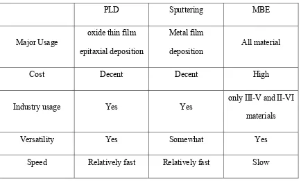
Table 2.1 Comparison of major deposition methods
PLD Sputtering MBE
Major Usage
oxide thin film
epitaxial deposition
Metal film
deposition
All material
Cost Decent Decent High
Industry usage Yes Yes
only III-V and II-VI
materials
Versatility Yes Somewhat Yes
Speed Relatively fast Relatively fast Slow
A variety of thin film deposition techniques have been employed for the preparation of
oxide films similar to what are presented in this dissertation. Of all the techniques, PLD and
MBE have yielded the best quality epitaxial films.
We use PLD as our primary sample preparation method. Some of the important factors
intensity of the laser power, photon frequency, ambient pressure, the choice of substrate,
substrate temperature, and post-deposition annealing.
2.2 Deposition Principles and Deposition System
Thin film formation during PLD generally can be divided into the following four stages:
1. Laser radiation interaction with the target,
2. Formation of ablation plume,
3. Deposition of the ablated materials onto the selected substrate,
4. Nucleation and growth of thin film.
At Stage 1, high power pulsed laser beam ejects material from a small amount of area of
the solid pellet target inside a high vacuum chamber. The absorbed energy is sufficient to break
any chemical bonds of the molecules of target material, which are subsequently deposited as a
thin film on a substrate. Usually, lasers with shorter wavelength (UV region) are preferred
because at shorter wavelengths the energy of the photons are higher and the ablation occurs more
efficiently. The fluence of a laser pulse [laser intensity, [J/cm2]] has to be larger than a threshold
value so that all the species can be stoichiometrically removed from the target.
At stage 2 - 4, the particle cloud absorbs a large amount of energy from the laser beam
producing an expansion of hot plasma (plume) in the deposition chamber. The ablated species
condense on the substrate placed opposite to the target, forming a thin film after some hundreds
The schematics of a typical set up of a PLD system is shown in Fig. 2.1. It includes the
laser system, deposition systems, and vacuum system which will be further discussed in sections
2.2.1, 2.2.2 and 2.2.3, respectively.
Fig.2.1 Basic set up for Pulsed Laser Depostion
2.2.1 Lasers
In general, the useful range of laser wavelengths for thin-film growth by PLD lies
between 200 nm and 400 nm. Most target materials used for deposition exhibit strong absorption
in this spectral region. Both excimer and Nd 3+:YAG laser are used as the laser source.
The excimer laser is a gas laser system; it emits radiation directly in the UV. These
systems have high outputs delivery and achieve pulse repetition rates up to several hundreds
Hertz with energies near 1 J/ pulse. Excimer KrF has the highest gain among systems with
wavelength 248 nm.
Nd 3+:YAG lasers are solid state alternatives to excimers lasers that are increasingly being
used in research laboratories. The neodymium ions serve as the active medium and are present
as impurities in the YAG host. The neodymium ions are pumped optically into their upper states
by flashlamps. High output energies are achieved by using two YAG rods in an
oscillator/amplifier configuration. The fundamental laser emission of Nd 3+:YAG occurs at 1064
nm, which can be frequency doubled with about 50% power conversion efficiency yielding an
output at 532 nm. With further doubling the frequency, the outputs at 355 nm or 266 nm are
produced.
2.2.1.2 Laser-Target Interaction
The interaction between laser pulses and the target depends strongly on the intensity of
the incoming laser beam in addition to wavelength. In PLD, the intensity is typically brought to
The mechanisms energy transferred to the target can be understood as follows: The
photon energy is initially absorbed by ionization and electronic excitation. After a few
picoseconds, the energy is transferred to the crystal lattice, and during the laser pulse, within a
few nanoseconds, a thermal equilibrium between the electrons and the lattice is reached. This
leads to a strong heating of the lattice and, with continued irradiation, to a massive particle
emission from the surface.
2.2.2 Deposition Systems
Fig. 2.2 Sketch of a PLD deposition chamber
The temperature of deposition also needs to be selected appropriately. In our experiment,
for epitaxial growth of rutile structure thin films, the substrates were heated 700 C. Some target
materials are quite sensitive to a change in the deposition temperature; a decrease of only a few
the film. A lower temperature also increases the formation of particulates and lattice defects. In
our experiment, the thin films become amorphous structure if grown at temperature 300 C.
To obtain epitaxial growth, the lattice structures of the substrate and expected thin film
need to be match with each other. The uniformity and crystallinity of the film can be further
increased by rotating the target (360° endless) during the deposition process (so that laser pulses
will not strike all the time the same spot on the target surface).
The oxygen pressure inside the chamber can be adjusted in order to accommodate
growing of different oxide films. The laser-pulse repetition rate is adjusted so that it is low
enough for the ablated species to have time to form a smooth layer between successive pulses.
Too low a repetition rate has to be avoided since fast chemical reactions may hinder the epitaxial
growth of the film. Pulse duration of the laser, repetition rate and spot size on the target also
need to be optimized in order to minimize the number of particulates that come out of the target
surface when collecting too much of energy in a single pulse.
2.2.2.1Ablation Plume
Some atoms in the vapour from the ejected material are ionized. The particle cloud
absorbs energy from the laser beam and becomes more ionized. Finally, fully ionized plasma is
formed in the vicinity (about 50 µm) of the target16. The plasma expands away from the target,
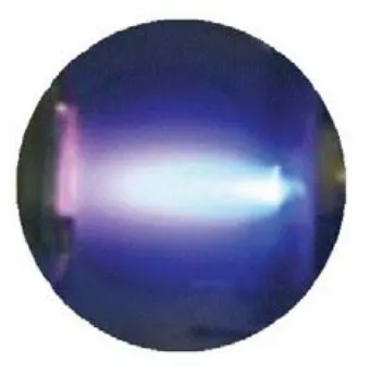
with a strongly forward-directed supersonic velocity distribution. A photograph of the plume is
shown in Fig. 2.3, The visible part of the particle jet is referred to as an ablation plume. The
plume consists of several types of particles: neutral atoms, electrons, and ions. Furthermore,
clusters of different compounds of the target elements are observed near the target surface. The
Fig. 2.3 Photograph of the plume17
2.2.3 High Vacuum System
High vacuum (HV) is the regime characterized by pressure from 1×10⁻³ to 1×10⁻⁹ Torr
(100 mPa to 0.1 µPa). HV requires the use of special materials, cleanliness, and baking the
entire system to remove water and other trace elements. Pressure is measured by an ionization
vacuum gauge. At low pressure, gas molecules rarely collide. The mean free path of a gas
molecule at 10-5 Pa (~10−7 Torr) is approximately 40 km, so gas molecules will collide with the
chamber walls many times before colliding with each other. Almost all interactions therefore
take place at various surfaces in the chamber.
HV is necessary for our thin film growth to reduce surface contamination, by reducing the
number of molecules reaching the sample over a given time period. At 0.1 mPa (10−6 Torr), it
only takes 1 second to cover a surface with a contaminant, so relatively lower pressures are
needed for long experiments to minimize the contamination of the films.
• High pump speed
• Minimized surface area in the chamber
• High conductance tubing to pumps — short and fat, without obstruction
• Use low-outgassing materials such as certain stainless steels
• Avoid creating pits of trapped gas behind bolts, welding voids, etc.
• Electropolish all metal parts after machining or welding
• Use low vapor pressure materials (ceramics, glass, metals, teflon if unbaked)
• Bake the system (250 °C to 400 °C) to remove water or hydrocarbons adsorbed to
the walls
• Chill chamber walls to cryogenic temperatures during use
• Avoid all traces of hydrocarbons, including skin oils in a fingerprint — always
use gloves
In our setup, base vacuum pressure during deposition better than 10-7 Torr is ensured by
the Turbo V-550 turbo molecular pump (Varian Vacuum Products), which is supported by a
mechanical fore-pump. Deposition can be made in vacuum or in the presence of reactive gases
with pressures up to a few mTorr.
2.3 Film Growth by Pulsed Laser Deposition.
High-temperature O-DMS films have been grown successfully on many different
substrates. A general requirement for a good substrate material is that, for certain orientations,
the lattices of the substrate and film match. Thermal expansion coefficients of the materials
should also be close such that the film does not break during the cool down to low temperatures.
If the mismatch of either of these parameters is large, the maximum thickness of the film that can
be grown epitaxially, if at all, is limited. Furthermore, a proper substrate material does not react
chemically with the film and preferably is compatible with semiconductor technology. In
addition, device applications impose a number of additional requirements on the substrate.
Depositing films on these substrates is a rather straightforward process and, therefore, they are
used in the preparation of several microelectronic components. On the other hand, the films
often have a large dielectric constant, which should be taken into consideration.
Substrates we use include R-plane -Al2O3 (012) for SnO2 film deposition and Si (400),
Al2O3 (012) and LaAlO3 (100) for HfO2 film deposition
2.4 Thin Film Characterization
2.4.1 X-Ray Diffraction
X-ray diffraction (XRD) is one of the most important non-destructive tools to analyse all
kinds of materials - ranging from films to powders and crystals. From research to engineering
and production, XRD is an important tool for materials characterization and quality control. In
our research, we use a Philips X’pert PW3040 MPD diffractometer using Cu Kα to identify the
2.4.2 Physical Properties Measurement System (PPMS)
Physical properties measurement system (PPMS) manufactured by Quantum Design was
used to make most of the electron transport measurements. The specific equipment used was
Model 6000 PPMS. This model allows for variable temperature and magnetic field
measurements. The temperature range is from 1.9 K to 400 K, and the magnetic field can go up
to 14 T. The cooling of the PPMS and the superconducting magnet inside is via liquid helium
introduced into a region called cooling annulus (shown in figure 2.5).
Figure 2.5: Cutout diagram of PPMS 6000 by Quantum Design [Copyright Quantum
2.4.3 Superconducting Quantum Interference Device (SQUID)
Fig.2.6 SQUID equipment (MPMS XL-7T, Quantum Design, Inc)
SQUID utilizes the superconducting quantum interference effect and can make the most
sensitive magnetic measurements to date. The MPMS-XL7 from Quantum Design, Inc (Fig. 2.6)
is capable of changing the magnetic field between -7 to 7 Tesla. The measurements can be
carried out at any temperature with accurate temperature control from 1.9 to 400 K. The
differential sensitivity is 10-8 emu and the instrument can make both DC & AC susceptibility
The four-point-probe method was used to measure the electrical transport properties of
the thin films. Fig. 2.7 shows a schematic diagram of the four-point-probe measurement set-up.
In the figure shown, the current is applied through probes 1 and 4 and the voltages measured
between probes 2 and 318.
Figure 2.7: Schematic of a four-point-probe measurement set-up for a thin film
2.4.4 Transmission Electron Microscope (TEM)
Transmission electron microscope (TEM) operates on the same basic principles as the
light microscope but uses electrons instead of light. Therefore TEM is limited by the wavelength
of the electrons. TEMs use electrons as the "light source" and their much lower wavelength
makes it possible to get a resolution a thousand times better than with a light microscope. We
can see objects at a scale of a few angstroms.
A "light source" at the top of the microscope emits the electrons that travel through
vacuum in the column of the microscope. Instead of glass lenses focusing the light in the light
microscope, the TEM uses electromagnetic lenses to focus the electrons into a very thin beam.
The electron beam then travels through the specimen one wants to study. Depending on the
At the bottom of the microscope the unscattered electrons hit a fluorescent screen, which gives
rise to a "shadow image" of the specimen with its different parts displayed in varied darkness
according to their density. The image can be studied directly by the operator or photographed
with a camera19.
Fig. 2.9 Transmission Electron Microscope
The TEM we use is a JEOL 2010 Transmission Electron Microscope, which has a wide
range of capabilities such as high-resolution image observation with 0.23 nm point resolution and
0.14 lattice image, EDS (Energy dispersive X-ray spectrometry) for element analysis, and
versatile analysis by electron diffraction. The magnification goes from 1,500 to 1,200,000×. The
Maximum accelerating voltage is 200kV.
CHAPTER 3
THE STRUCTURE AND MAGNETIC PROPERTIES OF TIN DIOXIDE THIN FILMS
3.1 Introduction
In the studies of room-temperature ferromagnetism (RTFM), there are various types of
transition-metal (TM) doped-oxide thin films, such as TM-doped ZnO, TM-doped TiO2, or
TM-doped SnO2. There are a number of controversial issues that need to be clarified20: for example,
why a clear correlation between the Curie temperature TC and the concentration of the magnetic
dopant element has not been established; and why doping by nonmagnetic elements, such as V
and Cu21, can sometimes result in strongly ferromagnetic samples; why, in some cases, bulk
samples are not magnetic but the thin films of the same compositions are magnetic. In these
materials, the ferromagnetism cannot simply be attributed to a secondary phase, although
existing theories of magnetism can not explain it. Several mechanisms are possible: carrier
mediated exchange coupling, spin polarons, short range superexchange, and defects induced
magnetism. Furthermore, in DMS, nonmagnetic host ions are partially substituted by the
magnetic dopants, which are randomly localized over the host lattice. Thus, it is difficult to use a
simple theory to completely explain everything.
Following the initial discovery of room temperature ferromagnetism in Co-doped TiO2 of
anatase structure, ferromagnetism was also found in doped TiO2 rutile thin films. The latter
seems more interesting from many perspectives. For example, the anomalous Hall Effect22, a
simultaneously observed in rutile films that exhibit ferromagnetism24. Researchers are thus
looking at other materials having the same rutile-type structure.
SnO2 a wide band gap semiconductor with Eg=3.6 eV25, and up to 97% optical
transparency in the visible range, crystallizes in rutile structure, Measurements of magnetic
properties of TM doped SnO2 vary vastly. Mn-doped SnO2 was reported to show a large
magnetoresistance at low temperature and paramagnetic behaviour26. While others reported that
it is ferromagnetic with TC equal to 340 K27. Fe and Co-doped SnO2 have been found to be
ferromagnetic with TC ranging from 360 K to 650 K.28,29, 30 Co-doped films have a rather high
magnetization of 7.5µB per Co and 7.5µB per Co respectively.31,32 Ni-doped SnO2 was reported to
have a TC = 400 K and magnetization of 2µB per Ni.33, 34, 35 Some synthesized powder36 such as
Sn0.99Fe0.01O2 also showed high Curie temperature TC=850 K. Much of these results are still
controversial due to the difficulty in resolving the true origin of the observed magnetic signals.
In order to clarify the confusion about these experimental results and for the reasons given above,
we have investigated Cr and Fe doped SnO2 films grown by PLD and studied their magnetic and
Fig. 3.1 Rutile structure SnO237
3.2 Experiments
FexSn1–xO2 and CrxSn1–xO2 (x = 0, 0.02, 0.06, 0.10, 0.20) thin films were grownon
-Al2O3 (012) substrates by PLD. Before deposition, the substrates were put in strong acid (HCL :
HNO3 ~ 3: 1) for 20 hours, to remove the weak ferromagnetic signal (about 10-5 emu) found in
the as-purchased substrates. The targets wereprepared using standard ceramic techniques. The
films were prepared in vacuum at a substrate temperature of 970 K. The pressure during
deposition was 2×10⁻⁶ Torr. The pulsed excimer laser uses KrF( = 248 nm) and produces a
laser beam of intensity (fluence) of 1–2 J/cm2 and repetition rate of 10 Hz. The Fe concentration
of thefilms was measured with energy dispersive x-ray analysis in TEmode, and was consistent
with those of the targets. The crystal structure was investigated by x-ray diffraction (XRD) with
interference device (SQUID) magnetometer. The transport properties were measured with a
physical property measurementsystem (PPMS) from Quantum Design.
3.3 Results and Discussion
Fig.3. 4 Interplanar spacing of (101) plane as a function of Cr concentration.
Solid line is the theoretical value and dots are our experimental results.
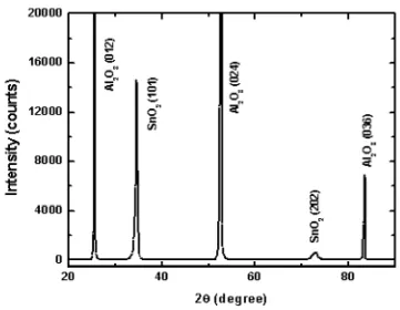
Figure 3.3 showsthe XRD pattern for a Cr0.2Sn0.8O2 film grown on R-plane -Al2O3
(012). The film is single phase and of rutiletype with (101) plane parallel to the film plane. The
two peaksshow (101) and (202) reflections of doped SnO2. The other threepeaks are fromthe
substrate -Al2O3 (012), (024) and (036). Similar XRDpatterns were obtained for all films with
consistent with the work of other groups.11, 10 For Fe-doped SnO2 films with fast deposition rate,
XRD patterns reveal impurity phases in the films.
Detailed study of SnO2 (101) and (202) peaks of CrxSn1–xO2 thin films reveals that they
have a systematic shift toward higher angles, which means that the interplane spacing decreases
continuously with the increase of Cr concentration (See Figure 3.4). CrO2 also crystallizes in
rutile structure. If we assume that Cr substitutes Sn continuously in SnO2, the interplanar spacing
should exhibit a linear change with Cr concentration as is indeed shown in Figure 2. This clearly
indicates that Cr dissolves in SnO2. On the other hand, for Fe doped SnO2 film, the interplanar
distance is almost independent of the Fe concentration, up to 20% doping. Since the radius of Sn
(IV) ion is 0.083 nm whereas the radii of Fe (III) and Fe (IV) ions are 0.069 and 0.0725 nm,
respectively, doping Fe in SnO2 should have resulted in a change of lattice parameter of SnO2.
Our XRD result does not indicate that Fe dissolves in SnO2.
The observation of room-temperature ferromagnetism in these materials must be
accompanied by a careful identification of the phases and microstructures present in order to
Fig. 3.5 Magnetization curves of Cr0.2Sn0.8O2 film measured at 5 K and room temperature.
Fig. 3.6 Cr0.2Sn0.8O2 ZFC-FC curves with H = 100 Oe.
Magnetic properties of Cr doped SnO2 films are shown in Fig. 3.5. The hysteresis loops
show that all Cr-doped films are paramagnetic at 300 and 5K, which is different from a recent
report.11 A very weak ferromagnetic signal of about 1×10⁻⁶ emu was observed in all Cr-doped
samples. Since this kind of signal also appears in pure SnO2 samples, we do not think it comes
from doped Cr. Both ZFC and FC curves (see Fig. 3.6) show a temperature dependence of
magnetic susceptibility that fits Curie-Weiss law, which is another evidence of paramagnetism in
Magnetic properties of Fe doped SnO2 films are shown in Figure 3.7. The hysteresis loop
exhibits ferromagnetic property at room temperature as reported previously. The coercivity of
the films is about 500 Oersted. At 5 K, the hysteresis loop exhibits similar behavior to the ones
at room temperature except that the coercivity increases to about 800 Oersted and magnetization
increases slightly. The magnetic moment per Fe atom is 1.0 µB/Fe. ZFC-FC curves exhibit a
blocking temperature of about 100 K. This blocking behavior implies that there are precipitated
ferromagnetic particles in the films which are partially responsible for the ferromagnetic property
of Fe-doped SnO2. The hysteresis observed at room temperature indicates that some larger
particles are not yet superparamagnetic and are still blocked.
The transport measurements indicate that the Fe doped SnO2 films have very high
resistance (about 107 ohm) at room temperature and the temperature dependence of the resistance
is characteristic of a semiconductor with an activation energy of about 230 meV (Figure 3.8).
The activation energy is sensitive to the oxygen pressure during the preparation, varying from
tens of meV (in vacuum) to hundreds of meV (in air) for pure SnO2, 39 and is also depend on the
doping elements and doping level. Coey et al. reported an activation energy of 75 meV in Fe
doped SnO2 after heating in vacuum12. It is not clear whether the observed value of 230 meV is
associated with the presence of Fe or the amount of oxygen vacancies. Neither
magnetoresistance signal nor anisotropic magnetoresistance (AMR) effect has been observed.
Fig. 3.8 Temperature dependence of resistance for Fe doped SnO2 film
3.4 Conclusions
We have prepared Cr and Fe-doped SnO2 films by PLD. X-ray diffraction patterns show
that the films are of rutile structure and grown along (101) plane. The diffraction peaks of
Cr-doped SnO2 exhibit a steady shift toward higher angles with increasing Cr concentration. This
indicates that Cr dissolves in SnO2. On the other hand, XRD experiments do not show similar
completely paramagnetic. The Fe-doped SnO2 samples are ferromagnetic at 300 and 5 K.
Zero-field-cooled (ZFC) and Zero-field-cooled (FC) curves indicate there are ferromagnetic particles in the
films which behave superparamagnetically above the blocking temperature of about 100 K. The
CHAPTER 4
ROLE OF DEFECTS IN TUNING FERROMAGNETISM IN DILUTED MAGNETIC
OXIDE THIN FILMS
4.1 Introduction
As discussed in chapter 3, we have synthesized the Cr and Fe doped SnO2 films which
were deposited on Al2O3 substrates by pulsed laser deposition. X-ray diffraction patterns show
that the films have rutile structure and grown epitaxially along (101) plane. The transport
measurements indicate that the Fe doped SnO2 thin films show high resistance (about 107 ohm) at
room temperature and the temperature dependence of the resistance is characteristic of a
semiconductor with calculated activation energy of about 230 meV. It is known that the
activation energy depends sensitively on the oxygen pressure during the preparation and varies
from tens of meV (in vacuum) to hundreds of meV (in air) for pure SnO2.40 It also depends on
the doping elements and doping level. Coey et al 41 reported an activation energy of 75 meV in
Fe doped SnO2 after heating in vacuum. Since we have not done a systematic study on the
oxygen content and Fe doping dependence of the activation energy, it is difficult to speculate
whether the observed value of 230 meV is associated with the presence of Fe. However, the
difference between the values of this study and Ref. 41 may suggest that our samples contain less
As mentioned in Chapter 3, the origin of the ferromagnetism at room temperature is still
an open question. Our previous study on Fe-doped TiO2 and other investigations suggest that
oxygen deficiency is important for the samples to exhibit ferromagnetism 2. Oxygen vacancies
were proposed as the origin for the ferromagnetism observed in undoped HfO2.42 Various
experiments and theoretical models suggest that oxygen vacancy may play a critical role in the
magnetism43,44,1. We continue this investigation and try to understand the relationship of oxygen
vacancy with respect to the magnetic properties in Cr doped SnO2 thin films.
4.2 Experiment
CrxSn1–xO2(x = 0, 0.02, 0.06, 0.10, 0.20) thin films were grown on -Al2O3 (012)
substrates invacuum at a substrate temperature of 970 K by PLD technique (KrF , = 248 nm, 1–
2 J/cm2 10 Hz.). Before deposition, the substrates were put in a strong acid (HCl: HNO
3 ~ 3: 1)
for 20 hours.
In order to elucidate the effects of oxygen vacancies on magnetism, selected samples of
Cr:SnO2 were also postannealed at 300 °C, 400°C, 500°C, 600°C during 10-12 hours in flowing
H2 atmosphere..
The Cr concentration of thefilms was measured with energy dispersive x-ray analysis in
TE mode, and they were consistent with those of the targets. The crystal structure was
investigated by x-ray diffraction (XRD) withCu K radiation. The magnetic propertieswere
studied with a superconducting quantum interference device (SQUID) magnetometer. The
transport properties were measured with a physical property measurementsystem (PPMS) from
interference device (SQUID) system from 5 K to 300K. For both magnetism and
magnetoresistance measurements, the magneticfield is applied in the film plane. Although the
samples with various Sn1–xCrxO2 compositions were prepared, here we mainly report the
experimental results of the Sn0.98Cr0.02O2 sample.
4.3 Experimental Results and Didcussion
4.3.1 SEM result
The microstructures of the samples were examined using scanning electron microscopy
(SEM). It is observed that heat treatment at different temperature of ambient have noticeably
different effects on the thin film. For annealing temperatures of 400°C and above, the thin films
were destroyed, as shown in the SEM photos in Fig. 4.1. At annealing temperatures below
Fig.4.1 SEM photos of Cr0.02Sn0.98O2annealed at temperatures of 600°C.
4.3.2 Magnetic properties
Figure 4.2 shows the comparison of the hysteresis loops measured at5 K and 300 K, after
and before the H2 treatment. The M[H] curves show a well defined hysteresis loop, note that the
shape of M[H] curves taken at 300 and 5K are quite similar indicating that the samples are
certainly in a ferromagnetic state over a certain range of temperature. The ferromagnetism is
clearly shown by the coercivity,remanence, and the low saturation field after H2 treatment in
both 5 K and 300 K. The data leads us to conclude that annealing in hydrogen leads to a
ferromagnetism, it may be attributed to the oxygen vacancies induced by the H2. The defect
levels created by the O vacancies can supply s, p carriers and lead to the spin-spin exchange
interaction between the s, p carriers and the localized d electrons of Cr. There may be also direct
d-d exchanges interaction between the neighbor Cr atoms if Cr atoms segregate in the host
lattice, however this latter scenario is less likely in our samples.
-1.0x10⁴ -5.0x10³ 0.0 5.0x10³ 1.0x10⁴
-4.0x10⁻⁵ -3.0x10⁻⁵ -2.0x10⁻⁵ -1.0x10⁻⁵ 0.0 1.0x10⁻⁵ 2.0x10⁻⁵ 3.0x10⁻⁵ 4.0x10⁻⁵ M (e mu)
Megnetic Field (Oe)
Before treatment measured at 5 K Before treatment measured at 300 K After treatment measured at 5 K After treatment measured at 300 K
Figure 4.2 The comparison of hysteresis loops measured at 5K and 300 K, after and
4.3.3 Resistance vs Temperature
160 180 200 220 240 260 280 300
0.0 5.0x10⁵ 1.0x10⁶ 1.5x10⁶ 2.0x10⁶ 2.5x10⁶ 3.0x10⁶ Re sistance ( Oh m ) Temperature
Before H2 treatment After H2 treatment
Fig. 4.3 Resistance vs Temperature of 2% Cr doped thin film before and after H2
treatment under 300°C
The film has the resistivity in the range of semiconductor and shows semiconducting
temperature dependence in Fig. 4.3 and the magnetic moment increase after the H2 treatment.
Fig. 4.4 indicates that the activation energy of the Cr-doped SnO2 films dropped from 81.506
meV to 47.076 meV when using 0
1
ln
R
ln
R
E
ak T
=
+
within temperature range from 160K to300K. Therefore, we conclude that the annealing in a reducing atmosphere does decrease the
activation energy as a result of increased oxygen vacancies in the films, and changes the
0.0030 0.0035 0.0040 0.0045 0.0050 0.0055 0.0060 0.0065 59874.14172
162754.79142
Ln(R
)
1/T
Fig. 4.4 Linear fit for Cr-doped SnO2 thin film before H2 treatment at higher temperature
from 160K to 300K Label axes
4.4 Conclusions
In summary, Sn0.98Cr0.02O2 magnetic semiconductors were synthesized. Composition
analysis and XRD patterns indicated that Cr element was incorporated intoSnO2. The film
obtained after H2 treatment is ferromagnetic at room temperature as confirmed by the magnetic
hysteresis curves shown in Fig. 4.2, it is also confirmed by the ZFC-FC results. From our
transport measurement, we calculated the activation energy, which did decrease from 81.506
meV to 47.076 meV, which can be explained by the increase in the defects/oxygen vacancies by
H2 treatment of the films. In this system, local Cr atoms may establish long range ferromagnetic
interaction between the neighbouring Cr atoms. The anisotropic magnetoresistance (AMR) was
not observed in the samples.
We also attempted to repeat the similar H2 treatment in our 6% Cr doped thin film
CHAPTER 5
STRUCTURE AND MAGNETIC PROPERTIES OF PURE AND
GADOLINIUM-DOPED HAFINIUM DIOXIDE THIN FILMS
5.1 Introduction
HfO245, CaB6 46,47 , 48 ,49 and CaO50 have been found, or predicted, to exhibit unusual
ferromagnetic behaviors, which can not be explained by the conventional mechanisms for
ferromagnetism (ferromagnetism contributed by magnetic ions). Theoretical calculations
indicate their ferromagnetism may be related to cation or anion vacancies. It has been proposed51,
52 that thin film deposition processes may create necessary oxygen vacancies to provide carriers
and induce magnetic moments, which establish magnetic states. Such hypothesis is currently
being debated and demands experimental study.
HfO2 is a wide-band insulator with high dielectric constant. The possibility of making the
material ferromagnetic may widen their applications in spintronics. As nonmagnetic as HfO2 is,
the discovery of ferromagnetic phenomenon in pure thin films53 was a surprise. These films are
found ferromagnetic, with a Curie temperature exceeding 500 K and a magnetic moment of about
anisotropic, being up to three times greater when the magnetic field is applied perpendicularly to
the plane of the film than when it is applied in the parallel direction.
Since dielectric oxide HfO2films, where neither Hf4+ nor O2– is magnetic, may leave Hf
atoms with an empty d shell, the phenomenon was initially termed d0 magnetism. It was
suggested that the magnetism probably arose from partially filled d orbitals originating from
hafnium atoms coordinating oxygen vacancies (VO). The isolated cation vacancies in HfO2
could form high-spin defect states, and therefore, could be coupled ferromagnetically with a
rather short-range magnetic interaction resulting in a ferromagnetic state
In this chapter, I report the synthesis of pure and Gd-doped HfO2 powders and thin films
and discuss their structure, transport and magnetic properties. The goal is to investigate the
effects of defects, controlled through annealing, on the magnetic properties of both the thin films
and powers.
5.2 Pure HfO2 Thin Films
5.2.1 Experiments
Pure and Gd-dopedHfO2 targets were prepared by standard ceramic techniques using
both 99.99% and 99.995%pure HfO2 and 99.99% pure Gd2O3 powders. The thin films were
deposited on single crystal silicon(400), R-Al2O3 (012), and LaAlO3 (100) substrates using a KrF
excimer laser with substrate temperature of 700±20 °C. The laser was operated at 10 Hz and was
focused through a 30 cm focal length lens onto a rotatingtarget at 45° angle of incidence. The
target-to-substrate distance was about 3 cm. Films were deposited with a base pressure of 5×10⁻⁷ Torr at
a growth rate of about 0.15 Å/s.
The crystal structure of the films was investigated by x-ray diffraction (XRD) with
Cu K radiation and high resolution transmissionelectron microscopy (HRTEM) with energy
dispersive spectroscopy (EDS). The magneticproperties were studied with a superconducting
quantum interference device (SQUID) magnetometer.
5.2.2 Structure Analysis
Figure 5.1 is the XRD pattern of a pureHfO2 thin film deposited on Si (400) substrate.
Besides Si substrate peaks, the rest peaks match the simple monoclinic phaseof HfO2. Similar
FIG. 5. 1 XRD pattern of a pure HfO2 thin film.
High resolution transmission electron microscopy images (Fig.5.2) show a columnar
structure in the HfO2 films, and the film thickness is typically in the range of 200 nm. The
thickness is also confirmedby Rutherford backscattering spectrometry (RBS). RBS results also
5.2.3 Magnetic Properties
Fig. 5.3 shows that the thin film is ferromagnetic at 300 K and 5 K for the pure HfO2
(pureness 99.95%) film deposit on Si substrate. The magnitude of the observed magnetic
moments is in the order of 10-6 emu. Fig. 5.4 show magnetization anisotropy of the thin film,
which is approximately tripled when the magnetic field is applied perpendicularly to the plane of
the thin film than applied in parallel, and this agrees with the result of Venkatesan et al.1
The anisotropy discussed above (Fig. 5.4), with magnetic field applied perpendicular and
parallel to the thin film, was measured by inserting a 5×3 mm film sample into the measuring
plastic straw. Two holes were cut on the straw to hold the sample in place. To investigate this
further, we have measured the film with “complete” plastic straw (without two cuts). The results
suggest the straw with holes itself introduces the “anisotropy”. The M-H curves of the straw
-10.0k -5.0k 0.0 5.0k 10.0k -1.2x10⁻⁵ -1.0x10⁻⁵ -8.0x10⁻⁶ -6.0x10⁻⁶ -4.0x10⁻⁶ -2.0x10⁻⁶ 0.0 2.0x10⁻⁶ 4.0x10⁻⁶ 6.0x10⁻⁶ 8.0x10⁻⁶ 1.0x10⁻⁵ Ma gn etizati o n ( e m u ) H (kOe) M300K' M5K'
-10.0k -5.0k 0.0 5.0k 10.0k -1.2x10⁻⁵ -1.0x10⁻⁵ -8.0x10⁻⁶ -6.0x10⁻⁶ -4.0x10⁻⁶ -2.0x10⁻⁶ 0.0 2.0x10⁻⁶ 4.0x10⁻⁶ 6.0x10⁻⁶ 8.0x10⁻⁶ 1.0x10⁻⁵ 1.2x10⁻⁵
H // film, complete straw H // film, straw with two cuts H ⊥film, staw with two cuts
M (emu
)
H (k Oe)
Fig. 5.4 magnetization of the thin film anisotropy
5.2.4 Signals From The Substrates
The method normally employed to measure the magnetic signal from the thin film is to
subtract the signal of substrate from that which combines the substrate and thin film. Fig. 5.5 is
the magnetization curve of Al2O3 substrate alone, which shows that the substrate itself has a
magnetic signal comparable to our HfO2 thin film on the Al2O3 substrate. This casts doubt on the
acid, the magnetization curve (Fig. 5.6) showed a dramatic decrease in the magnetic signals,
from 10-5 emu down to 10-7 emu, which confirmed that there were magnetic impurities on the
substrate. A similar signal difference before and after the acid wash was also confirmed for Si
substrates. Thereafter, all substrates for deposition were cleaned in strong acid (HCl:
HNO3~3:1) for 20 h to get rid of the magnetic impurities.
Fig. 5.6 Al2O3 substrate with acid wash.
HfO2 powder of purity 99.95% is not the purest available, and the most likely impurity is
ZrO2. ZrO2 thin film was deposited on the Si substrate under the same conditions as HfO2. Fig.
5.7 shows the weak magnetic signal at 10-6 emu, which is in the same order of magnitude as the
thin film shown in Fig. 5.4. The above data do not suggest ZrO2 is ferromagnetic, rather they
-10.0k -5.0k 0.0 5.0k 10.0k
-4.0x10⁻⁶
-2.0x10⁻⁶
0.0
2.0x10⁻⁶
4.0x10⁻⁶ ZrO2/Si
Si substrate
M (emu)
H (K Oe)
Fig. 5.8 The magnetizationcurves measured at 300 and 5 K for the purer HfO2(purity:
99.995%) film on Si substrate.
The effect of the purity of the raw HfO2 was investigated. Figure 5.8 shows the
magnetizationcurves measured at 300 and 5 K for films made of purer HfO2(purity = 99.995%)
grown on Si substrate. An extremely weak ferromagnetic signal of about 5×10⁻⁷ emu was
observed. If we assume that the measured signal is attributedto the HfO2 films, the moment of
value. Moreover, considering the contribution from either the impuritiesin the target material or
the residual impurities on the substrates,we conclude that our as-deposited HfO2 films itself are
not ferromagnetic.
The possible effects of defects/oxygen vacancies were studied on an as-deposited HfO2
films by annealing it in air at 1000 oC, in an attempt to change the amount of oxygen vacancies.
As shown in Fig. 5.9, no visible changes in the magnitude of the magnetization was seen. The
mechanism for magnetism in these thin films appears not intimately connected to the defects or
oxygen vacancies. Our study described above suggests that one needs to be extremely careful
Fig. 5.9 Magnetization for HfO2 film grown on Al2O3 annealed at 1000 oC.
5.3 Gd Doped HfO2 Thin Film
As a wide band gap dielectric material with nonmagnetic4f14.5d2.6s2 configuration, HfO2
itself contributes no net moment. Theoretically, the medium of exchange by small amounts of
impurity of the 4f band structure leads to 4f to 5d intra-atomic hybridization, and overlap with
the unoccupied band structure just above the Fermi level, which may result in net overall
relatively large magnetic moment among the rare earth elements, was chosen as the impurity to
be doped in our HfO2 thin film.
Fig. 5.10 is the XRD pattern of a Gd doped HfO2 thin film deposited on Si (400)
substrate. Other than the Si peaks from the substrate, all peaks match those of the simple
monoclinic phase of HfO2. Gd-doped HfO2 thin films have the same XRD pattern except that
their diffraction peaks have a small shift toward lower angles. For example, (111) peak is shifted
by 0.18° from 28.29° to 28.11°, which means that the lattice parameter increases after the Gd
doping. The ionic radii of ionized Gd (Gd3+) are 0.1078 nm (six coordinate) and 0.1193 nm
(eight coordinate), whereas the ionic radii of Hf4+ are 0.085 and 0.097 nm for the corresponding
coordinates. Since the radii of Gd3+ are larger than those of Hf4+, our XRD result implies that Gd
Fig. 5. 10 XRD patterns of a pure and Gd-doped HfO2 thin film.
The film exhibits obvious paramagnetic signal, instead of ferromagnetic behaviour, in
Fig. 5.11 (a) The magnetization curves at 300 and 5 K.
5.4 Defects Hypnosis
5.4.1 HfO2 Thin Film
Different substrates should result in different interfaces and defect structures at the
interfaces between the thin film and substrate, which may bethe source of the ferromagnetism.4,55
In orderto alter the interface structure between the film and substrate, HfO2 films were deposited
on Al2O3 (012) andLaAlO3 (100) substrates in addition to Si substrate. Our experiments (shown
in Fig. 5.12) suggest no obvious difference in the magnetic properties of theHfO2 films deposited
Fig. 5.12 Magnetization curve for HfO2 film grown on LAO
All thin films were annealedin air at 700, 900, and 1000 °C to determine if annealing
might change the defects in the HfO2 films andinfluence their magnetic behaviour. In otherwise
nonmagnetic compound suchas CaB6 and CaO, like HfO2, the magnetismis considered to be
driven by intrinsic point defects. However,the magnetic signal observed did not change with
HfO2 films were also deposited at room temperature in order to vary the defect density in
the films. The filmswere found to be amorphous by XRD measurements. The magneticsignal
was extremely weak, in the magnitude of 10-6 emu.
5.4.2 HfO2 Powder
In addition to the films, HfO2 powders of different purity were annealed at different
temperature (700, 900, and1100 °C) and in different atmospheres. XRD measurement indicates
that thereis no phase change for the HfO2 powders after annealing under different atmospheres
(shown in Fig. 5.13). Magnetic measurements show that neither the original powders nor
annealedones are ferromagnetic. The defects introduced by hydrogenreduction carried out here
Fig. 5. 13 XRD measurements for the HfO2 powders before (E-) and after annealing at Ar and H2
Fig. 5.15 Magnetization curves for 99.995% HfO2 power.
5.5 Conclusion
Our HfO2 films deposited on Si (400), Al2O3 (012) and LaAlO3 (100) substrates by PLD
do not exhibit ferromagnetic properties, which is different from some of the reported data. The
magnetic signal of the HfO2 films does not change significantly with annealing at various
in H2 flow) are not ferromagnetic. For Gd-doped (3%) HfO2 film, XRD result implies that Gd
dissolves in HfO2. The film exhibits paramagnetic signal at low temperature. ZFC-FC curves do