157
Copyright © 2017. Vandana Publications. All Rights Reserved.
Volume-7, Issue-5, September-October 2017
International Journal of Engineering and Management Research
Page Number: 157-162
0.5 V, Low Power Notch Based G
m-C Complex Filter Design for
Wireless Receiver
E.Lakshmi Prasanna1, T.Lilly prasanthi2 1
ECE Department, Universal College of Engineering and Technology, INDIA 2
Assistant Professor, ECE Department, Universal College of Engineering and Technology, INDIA
ABSTRACT
This paper presents a novel Gm
I. INTRODUCTION
C complex filter approach with high image rejection for standard wireless receiver applications.The filter is implemented with a new architecture in 130nm CMOS process.Since by conventional approach, to get more IRR, the order of the filter has to be increased, where as by using novel approach 55 dB IRR is achieved with a just a second order Complex band pass filter and a first order complex notch filter. By using this novel architecture the desired IRR band can be achieved with less number of stages with improved complex band pass response.The quality factor is improved and power consumption is also reduced when compared with the conventional approach design. In this paper the novel architecture is designed for blue tooth low energy receiver applications with center frequency of 4MHz and bandwdth of 2MHz with power consumption of 54 W.To consume low power a novel design of Operational Trans conductance amplifier with bulk driven is proposed with a 0.5 V supply in this paper.
Keywords— Image Rejection Ratio, Complex Filter,
Oper-ational transconductance amplifier, Source degeneration, Blue-tooth
Now a days for most of the wireless receiver technologies uses IF(Intermediate Frequency) stage in the analog signal processing hence most of the architectures may has the image frequency band problem.This problem can be avoided by increasing the number of IF stages or by using very high Q(Quality Factor) Value. Larger Q IF stages are not good for low CMOS technologies,because very high Q factor can be possible only with the SAW filters which can not be fabricated on the chip,Though the Gm
Fig. 1. Front end wireless Receiver
C filter can increase but very large capacitance is needed,for example to get Q value of 10 need to get 100 times more bigger capacitance as
compared with standard capacitance. Another way to suppress image signal is RF(Radio Frequency) frequency can be directly converted to base band frequency with out any IF stage. But this may increase the flicker noise which is more dominant for low frequencies.If directly base band conversion technique is used it is not suitable for bio medical applications because of their low frequency band i.e limited to 10Hz-3KHz.Fig 1 shows the standard front end wireless Receiver block diagram [1]after Low Noise Amplifier RF is down converted to IF in this process the unwanted signal frequency which is equal to IF frequency may enter into the mixer hence most of the wireless architectures need to have a complex filter or poly phase filter after the IF stage and before to analog to digital converter.
Fig. 2. Front end wireless Receiver
158
Copyright © 2017. Vandana Publications. All Rights Reserved.
A. Basics of Complex Filter
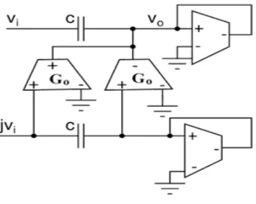
Complex filter is a frequency shifted band pass or band stop filter by using imaginary and real components of the input signal.Since the magnitude spectrum of any filter is symmetric and even hence it should have both positive and negative symmetric response.The image signal in the communication is negative frequency hence the attenuation of image band can be done by shifting the desired band of frequency to the right side by the frequency transformation.[2] [3][13]This can be implemented by both active RC and GmC filters because GmC complex filters use low-power and less chip area they are preferred. In order to get required image rejection ratio more cascaded stages have to be connected and in Active RC due to use of more passive components the noise will be more and dissipates more power hence using Active RC implementation draws more power,hence in low power applications GmC filter are useful,Fig 2 shows the mathematical analysis of rejecting the image signal by using complex filter.
B. Conventional Architecture For Complex Band pass Filter
A Conventional Complex band pass filter can be made by shifting the negative cutoff frequency of the low pass filter to the positive frequency.Using conventional GmC filters in order to get improved band pass filter response and high IRR, the order of the filter should be very high. Here the frequency transformation can be done by differential capacitance transformation [2] [4]that is in place of each capacitance the differential capacitance which is the combination of both negative and positive Gm should be used. The Conventional Approach for GmC realization for the fifth order Complex Bandpass Filter is shown in the Fig 3.That is A fifth order low pass ladder can be converted to a complex band pass by using in phase and quadrature phase blocks and each capacitance should be connected to parallel combination of positive and negative Gm to give differential Capacitance. where each Resistance and inductance is replaced by GmC cells by using gyrator principle.[5][6]
As shown in the Fig 3, the low pass response can be transformed to bandpass by using frequency right shifting. This shifting can be done by using both positive and negative Gm cells.WRE is the cutoff frequency of the low pass filter. WSHIF T is shifting frequency from low pass cutoff frequency. Shifting can be done by using GSHIF T cell.[7] [8]In this process in phase signal and quadrature signals has to be taken [9] [10]individually and each capacitance is converted to differential capacitance to get the band pass response as shown in the Fig 3.
C. Limitations of conventional Gm C Complex bandpass filter
Since by conventional approach of GmC complex band pass filter IRR is depends on the order of the filter i.e for more IRR the order of the filter has to be increased. Hence to attenuate image frequency signal more power will consume.[11]12The second limitation is in order to increase Q factor of this filter the value of GSHIF T is more compared to GRE so this is also will increase the power consumption. To overcome these limitations the novel complex Gm
III. NOVEL APPROACH OF COMPLEX
BAND PASS FILTER WITH REQUIRED
IMAGE REJECTION BAND
C filter gives good IRR band and improved band pass response.[1][2][4]
159
Copyright © 2017. Vandana Publications. All Rights Reserved.
with just a second order complex and one first order complexnotch filter hence no need to go for higher order filters.In this paper a second order conventional complex filter has taken as shown in the Fig 5 and the left shifted notch filter is shown in the Fig.6
A. New Complex Notch Filter
Complex notch filter is similar to complex band pass filter. In this high pass filter frequency response will be shifted with the amount of wo to the left side of the origin. The high pass filter with a low cutoff frequency alone can be used in the place of complex notch filter. But the design of GmC high pass filter with very low cutoff frequency is difficult because of high capacitance and low Gm is required. Since lower cutoff frequency of a High pass filter is proportional to Gm/C hence in order to achieve lower cutoff frequency around 45 KHz need to have very high capacitance more than 100 pF when Gm is tuned to 46 s or high Gm has to be required. High Gm can be achieved by increasing the bias tail current of OTA cell even though the effective Gm
Hence complex stop band or notch filter is used a, by observing the frequency response of this filter as shown in the Fig 10. the positive notch frequency is shifted to the left side as mentioned earlier, as capacitance decreases the notch shifting towards left side is also increases. one can get the desired notch response by tuning the capacitance by fixing the G
value is not sufficient to get very low cutoff frequency.
m. The cutoff frequency of the high pass filter is shifted towards the left side by a frequency wo as the equations written in the paper the transformation has done from high pass filter to the complex band reject filter. Where H(s) represents the transfer function of the first order GmC highpass filter and frequency shifting of this function to the left side by a wy
as mentioned in the above equation (4),the Complex notch filter is designed is shown in the Fig 7.The frequency response of this new notch filter shown in the Fig 11.Since shifting frequency depends on the G
represents first order complex notch filter. The shifting frequency is proportional to gm and inversely proportional to the capacitance as shown in the equation 3.This technique can be used for High frequency image rejection applications. The implementation of the Complex notch filter based on the following equations:
o and C hence to shift the frequency to left have to vary either Go or capacitance. For the first order at capacitance 1 pF notch frequency around 8 KHz is obtained if we decreasing the capacitance to 100 fF the notch frequency can be increased around 1 MHz. In this paper the first order notch filter is designed by using above equations that is by using positive G and negative G.The notch response of this filter with respect to capacitance can be observed in Fig 11.Notch filter alone can be used to suppress image frequency or electrical frequency 50 Hz where it is useful in bio medical applications, but it can not suppress image frequency with High IRR and that to it is limited to certain low bands. That is why the novel complex filter architecture will be useful in any frequency band of Image rejecting applications
B. Proposed Complex Bandpass Filter
As shown in the Fig 7, it is the multiplication of the two asymmetrical responses with the less filter order stages. i.e the cascaded connection of second order complex filter and first order notch filter will give the desired IRR .This filter operating at center frequency of 4 MHz has achieved more than 55dB IRR with improved band pass filter response. As shown in the Fig 5, H1
The second order low pass response, as shown in the equation(7) can be converted to complex bandpass response by shifting frequency to right .H
(S) shows the second order low pass response of the filter as shown in the Fig 3.
1(S sx
(8)is right shifted low pass response with a frequency of w ) is showing in equation
160
Copyright © 2017. Vandana Publications. All Rights Reserved.
and H2(S + sy is showing the frequency left shifted high passfilter i.e first order complex notch filter. The product of the second order complex band pass and first order complex notch filter response gives the desired novel complex band pass filter as shown in the below equation(14).
H1(S-sx) =
K
(8) 2
( S -sx)2 + 2K( S-sx) + K2
H2(S) =
S
(9)
S + K
H2(S + sy) =
(S + sy)
(10) K + (S + sy)
H1(S-sx).H2(S + sy) =
K2 (S + sy
(11) )
( (S-sx)2 + 2K( S -sx) + K2 . K + (S + sy) ) where s = jω and ωx is the right shifted frequency of second order complex band pass filter, similarly ωy is left shifted frequency of first order complex notch filter. In order to get desired IRR band and improved band pass response, the magnitude of !y is always less than magnitude of ωx.
While observing the stability of all filters are stable because of each filter mentioned in this paper has the poles in left half of the s plane, hence no need to compensate any pole of the system. While analyzing the equation one thing has to be remember i.e
the value of K is dependent on Gm and capacitance. As
capacitance is decreased the negative notch frequency will be increased, but a very low negative notch frequency is required for this proposed architecture. Hence the optimal value of the capacitance has to be chosen in this paper is 150 fF.
C. Proposed Operational transconductance amplifier used in this paper
The bulk driven Operational trans conductance amplifier(OTA) is proposed to operate in sub threshold region(weak inversion with 0.5V supply is shown in the Fig.8.This proposed OTA can be used for very low frequency as well as high frequency with varying transistor aspect ratio. All transistors in this OTA except M13,M14 are operating in sub threshold region. Transistors M13,M14 are operating in triode region to act as Resistance. This two resistance will give internal common mode feed back. Where as transistors M11,M12 are cross coupled to act as negative resistance. Because the bulk driven OTA will have less dc gain, that can be increased by using this negative resistance. Since most of the transistors are operating in weak inversion region the power consumed by the Gm cell is low. The input is given to PMOS transistors M3,M1 and M2,M24 where (W/L) of M3 is less than that of M1 similarly M2 is less than that of M4.NMOS transistors.
161
Copyright © 2017. Vandana Publications. All Rights Reserved.
IV.
RESULTS
162
Copyright © 2017. Vandana Publications. All Rights Reserved.
filter frequency response with capacitance tuning is shown inFig 10.The Second order conventional complex bandpass filter frequency response and phase response is shown in the Fig 11 and Fig 13 respectively. The first order complex notch filter frequency response and phase response is shown in Fig 12 and Fig 14 respectively.
V. V. CONCLUSION
The proposed Gm
[7] Nan Qi; Zheng Song; Baoyong Chi; Wang, A.; Tianling Ren; Zhihua Wang, ”A multi-mode complex bandpass filter
with gm-assisted power optimization and I/Q calibration,” in Circuits and Systems (ISCAS), 2013 IEEE International Symposium on , vol., no., pp.1845-1848, 19-23 May 2013
C Complex filter uses less number of filter stages and achieved 55 dB Image Rejection Ratio with the lower Order of three. When compared with the conventional filter i.e Only 39 dB IRR is attained by using Conventional approach second order Filter where as more than 55 dB IRR is attained with just a second order complex band pass filter and a first order complex notch filter. SFDR (Spurious Free Dyanamic Range) is 63.8 dB. the total power consumption of third order proposed complex bandpass filter is 54 W with a 0.5 V supply. This technique is also useful in the RF frequency applications.
REFERENCES
[1] Chuanchuan Wan; Zhiqun Li, ”A 2MHz CMOS Gm-C complex filter with on-chip automatic tuning for wireless sensor networks application,” in Communications, 2009. APCC 2009. 15th Asia-Pacific Conference on , vol., no., pp.199-202, 8-10 Oct. 2009
[2] Alzaher, H.A.; Alghamdi, M.K., ”Implementation of Compact Polyphase Channel-Select Filters for Multistandard Broadcasting,” in Very Large Scale Integration (VLSI) Systems, IEEE Transactions on , vol.23, no.10, pp.2312-2316, Oct. 2015
[3] Ao Li; Hong Zhang; Xunwei Weng; Ruizhi Zhang, ”A low-power Gm-R-C image rejection filter for complex low-IF receiver,” in ASIC (ASICON), 2011 IEEE 9th International Conference on , vol., no., pp.998-1001, 25-28 Oct. 2011 [4] Indner, B.; Wagner, J.; Joram, N.; Yodprasit, U.; Ellinger, F., ”Reconfig-urable complex gm-c band-pass filter with high linearity for multi-standard radio receivers,” in Intelligent Signal Processing and Communication Systems (ISPACS), 2014 International Symposium on , vol., no., pp.287-290, 1-4 Dec. 2014
[5] Abdelrahim, T.A.; Elesseily, T.; Ahmed Saad Abdou; Sharaf, K.M.W., ”A 12-mW Fully Integrated Low-IF dual-band GPS Receiver on 0.13-m CMOS,” in Circuits and Systems, 2007. ISCAS 2007. IEEE International Symposium on , vol., no., pp.3034-3038, 27-30 May 2007
[6] Nan Qi; Yang Xu; Baoyong Chi; Xiaobao Yu; Xing Zhang; Ni Xu; Chiang, P.; Woogeun Rhee; Zhihua Wang, ”A Dual-Channel Com-pass/GPS/GLONASS/Galileo Reconfigurable GNSS Receiver in 65 nm CMOS With On-Chip I/Q Calibration,” in Circuits and Systems I: Regular Papers, IEEE Transactions on , vol.59, no.8, pp.1720-1732, Aug. 2012
[8] Teo, T.H.; Khoo, E.-S.; Uday, D.; Tear, C.-B., ”Design, analysis, and implementation of analog complex filter for low-IF Wireless LAN application,” in VLSI Design, 2004. Proceedings. 17th International Conference on , vol., no., pp.416-421, 2004
[9] ahmy, M.M.; Mahmoud, Soliman A., ”A CMOS complex Gm C filter for low-IF bluetooth receiver,” in Microelectronics, 2008. ICM 2008. International Conference on , vol., no., pp.78-81, 14-17 Dec. 2008
[10] Guthrie, B., Hughes, J., Sayers, T. and Spencer, A., ”A CMOS gyrator low-IF filter for a dual-mode Bluetooth/ZigBee transceiver,” IEEE Journal of Solid-State Circuits, vol.40, no.9, pp.1872-1879, 2005.
[11] Tedeschi, M., Liscidini, A. and Castello, R., ”Low-Power Quadrature Receivers for ZigBee (IEEE 802.15.4) Applications,” IEEE Journal on Solid-State Circuits,, vol.45, no.9, pp.1710-1719, Sept. 2010
[12] Laoudias, C. and Psychalinos, C., ”Low-voltage Bluetooth/ZigBee complex filter using current mirrors,” IEEE International Symposium on Circuits and Systems (ISCAS), pp.1268-1271, 2010.