Programmable Logic Design
Quick Start Hand Book
By Karen Parnell & Nick Mehta
June 2003
Edition
ISE 5.1i
Whether you design with discrete logic, base all of your designs on microcontrollers, or simply want to learn how to use the latest and most advanced programmable logic software, you will find this book an interesting insight into a different way to design.
Programmable logic devices were invented in the late seventies and since then have proved to be very popular and are now one of the largest growing sectors in the semiconductor industry. Why are programmable logic devices so widely used? Programmable logic devices provide designers ultimate flexibility, time to market
advantage, design integration, are easy to design with and can be reprogrammed time and time again even in the field to upgrade system functionality.
This book was written to complement the popular Xilinx Campus Seminar series but can also be used as a stand-alone tutorial and information source for the first of your many programmable logic designs. After you have finished your first design this book will prove useful as a reference guide or quick start handbook.
The book details the history of programmable logic, where and how to use them, how to install the free, full functioning design software
(Xilinx WebPACK ISE included with this book) and then guides you through your first of many designs. There are also sections on VHDL and schematic capture design entry and finally a data bank of useful applications examples.
We hope you find the book practical, informative and above all easy to use.
Programmable Logic Design
Quick Start Hand Book
NAVIGATING THE BOOK
This book was written for both the professional engineer who has never designed using programmable logic devices and for the new engineer embarking on their exciting career in electronics design. To accommodate this the following navigation section has been written to help the reader decide in advance which section he/she wishes to read.
This chapter gives an overview of how and where programmable logic devices are used. It gives a brief history of the programmable logic devices and goes on to describe the different ways of designing with PLDs.
Chapter 2 describes the products and services offered by Xilinx to ensure PLD designs enable time to market advantage, design flexibility and system future proofing. The Xilinx portfolio includes both CPLD & FPGA devices, design software, design services & support, and Cores.
The WebPACK ISE design software offers a complete design suite based on the Xilinx Foundation ISE series software. This chapter describes how to install the software and what each module does.
Chapter 2 Xilinx Solutions Chapter 3 WebPACK ISE Design Software Chapter 1 Introduction
This section is a step by step approach to your first simple design. The following pages are intended to demonstrate the basic PLD design entry implementation process.
This chapter discusses the Synthesis and
implementation process for FPGAs. The design targets a Spartan IIE FPGA.
This section takes the VHDL or Schematic design through to a working physical device. The design is the same design as in the previous chapters but targeting a CoolRunner CPLD.
The final chapter contains a useful list of design examples and applications that will give you a good jump-start into your future programmable logic designs. It will also give you pointers on where to look for and download code and search for Intellectual Property (IP) Cores from the Xilinx Web site. Chapter 4 WebPACK ISE Design Entry Chapter 5 Implementing FPGAs Chapter 7 Design Reference Bank Chapter 6 Implementing CPLDs
ABSTRACT
NAVIGATING
THE
BOOK
CONTENTS
ABBREVIATIONS
Chapter 1 INTRODUCTION
1.1
The History of Programmable Logic
1.2 Complex
Programmable
Logic
Devices (CPLDs)
1.2.1
Why
Use
a
CPLD?
1.3
Field Programmable Gate Arrays
(FPGAs)
1.4
The Basic Design Process
1.5
Intellectual Property (IP) Cores
1.6 Design
Verification
Chapter 2
XILINX SOLUTIONS
2.1 Introduction
2.2 Xilinx
Devices
2.2.1 Platform FPGAs
2.2.2 Virtex
FPGAs
2.2.3 Spartan
FPGAs
2.2.4 Xilinx CPLDs
2.2.5 Military and Aerospace
2.2.6 Automotive and
Industrial
2.3 Design
Tools
2.4
Xilinx Intellectual Property (IP) Cores
2.5
Web Based Information Guide
2.5.1 ESP Emerging
Standards and
Protocols
2.5.2 Xtreme DSP
2.5.3 Xilinx On Line
2.5.4 Configuration Solutions
2.5.5 Processor Central
2.5.6 Memory Corner
2.5.7 DSP Central
2.5.8 Connectivity Central
2.5.9 Signal Integrity
2.5.10 Education Services
2.5.11 University Program
2.5.12 Design Consultants
2.5.13 Technical Support
Chapter 3 WebPACK
ISE DESIGN
SOFTWARE
3.1 Module
Descriptions
3.2
WebPACK Design Suite
3.3
WebPACK CDROM Installation
3.4
Getting
Started
Chapter
4
WebPACK
ISE DESIGN ENTRY
4.1
Introduction
4.2
Design
Entry
4.3
Functional
Simulation
4.4
State Machine Editor
4.5
Top Level VHDL Designs
Chapter 5
IMPLEMENTING FPGAS
5.1 Introduction
5.2 Synthesis
5.3 Constraints
Editor
5.4 Reports
5.5 Timing
Simulation
5.6 Configuration
Chapter 6
IMPLEMENTING CPLDS
6.1
Introduction
6.2 Synthesis
6.3
The Constraints File
6.4
CPLD
Reports
6.5
Timing
Simulation
6.6
Programming
Chapter 7
DESIGN REFERENCE BANK
7.1
Introduction
7.2
Get the Most out of
Microcontroller-Based Designs
7.3
Application Notes and Example Code
7.3 Website
Reference
ABEL
Advanced Boolean Expression Language
ASIC
Application Specific Integrated Circuit
ASSP
Application Specific Standard Product
ATE
Automatic Test Equipment
CDMA
Code Division Multiple Access
CPLD
Complex Programmable Logic Device
CLB
Configurable
Logic
Block
DCM
Digital Clock Manager
DCI
Digitally Controlled Impedance
DES
Data Encryption Standard
DRAM
Dynamic Random Access Memory
DSL
Digital Subscriber Line
DSP
Digital Signal Processor
DTV
Digital
Television
ECS
Schematic
Editor
EDA
Electronic Design Automation
FAT
File Allocation Table
FIFO
First In First Out
FIR
Finite Impulse Response (Filter)
Fmax
Frequency Maximum
FPGA
Field Programmable Gate Array
FSM
Finite State Machine
GPS
Geo-stationary Positioning System
GUI
Graphical User Interface
HDTV
High Definition Television
IP Intellectual
Property
I/O
Inputs and Outputs
IRL
Internet
Reconfigurable
Logic
ISP
In-System
Programming
IQ
Extended temperature devices for automotive
and industrial applications
JTAG
Joint Test Advisory Group
LSB
Least Significant Bit
LUT
Look Up Table
MP3
MPEG Layer III Audio Coding
MPEG
Motion Picture Experts Group
MSB
Most Significant Bit
NRE
Non-Recurring
Engineering
(Cost)
PAL
Programmable Array Logic device
PCB
Printed
Circuit
Board
PCI
Peripheral Component Interconnect
PCMCIA
Personal Computer Memory Card International
Association
PCS
Personnel Communications System
PLA
Programmable Logic Array
PLD
Programmable Logic Device
PROM
Programmable Read Only Memory
EPROM
Erasable Programmable Read Only Memory
RAM
Random
Access
Memory
ROM
Read Only Memory
SPLD
Simple Programmable Logic Device
SRAM
Static Random Access Memory
SRL16
Shift Register LUT
Tpd
Time of Propagation Delay through the device
UMTS
Universal Mobile Telecommunications System
VHDL
VHISC High Level Description Language
VHSIC
Very High Speed Integrated Circuit
VSS
Visual
Software
Solutions
WLAN
Wireless Local Access Network
XST
Xilinx Synthesis Technology
XCITE
Xilinx Controlled Impedance TEchnology
QML
Qualified Manufacturers Listing
QPRO
QML Performance Reliability of supply
Off-the-shelf ASIC
INTRODUCTION
The following chapter gives an overview of how and where
programmable logic devices are used. It gives a brief history of the programmable logic devices and goes on to describe the different ways of designing with PLDs.
1.1
The History of Programmable Logic
By the late 70’s, standard logic devices were the rage and printed circuit boards were loaded with them. Then someone asked the question: “What if we gave the designer the ability to implement different interconnections in a bigger device?” This would allow the designer to integrate many standard logic devices into one part. In order to give the ultimate in design flexibility Ron Cline from
Signetics (which was later purchased by Philips and then eventually Xilinx!) came up with the idea of two programmable planes. The two programmable planes provided any combination of ‘AND’ and ‘OR’ gates and sharing of AND terms across multiple OR’s.
This architecture was very flexible, but at the time due to wafer geometry's of 10um the input to output delay or propagation delay (Tpd) was high which made the devices relatively slow.
Figure 1.1 What is a CPLD?
MMI (later purchased by AMD) was enlisted as a second source for the PLA array but after fabrication issues was modified to become the Programmable Array Logic (PAL) architecture by fixing one of the programmable planes. This new architecture differs from that of the PLA by having one of the programmable planes fixed - the OR array. This PAL architecture had the added benefit of faster Tpd and less complex software but without the flexibility of the PLA structure. Other architectures followed, such as the PLD (Programmable Logic Device). This category of devices is often called Simple PLD (SPLD).
Figure 1.2 SPLD Architectures
The architecture has a mesh of horizontal and vertical interconnect tracks. At each junction, there is a fuse. With the aid of software tools, the user can select which junctions will not be connected by “blowing” all unwanted fuses. (This is done by a device programmer or more commonly nowadays using In-System Programming or ISP). Input pins are connected to the vertical interconnect and the
horizontal tracks are connected to AND-OR gates, also called
“product terms”. These in turn connect to dedicated flip-flops whose outputs are connected to output pins.
PLDs provided as much as 50 times more gates in a single package than discrete logic devices! A huge improvement, not to mention fewer devices needed in inventory and higher reliability over standard logic.
Programmable Logic Device (PLD) technology has moved on from the early days with such companies as Xilinx producing ultra low power CMOS devices based on Flash technology. Flash PLDs provide the ability to program the devices time and time again
electrically programming and ERASING the device! Gone are the days of erasing taking in excess of twenty minutes under an UV eraser.
1.2 Complex Programmable Logic Devices (CPLDs)
Complex Programmable Logic Devices (CPLD) are another way to extend the density of the simple PLDs. The concept is to have a few PLD blocks or macrocells on a single device with general purpose interconnect in between. Simple logic paths can be implemented within a single block. More sophisticated logic will require multiple blocks and use the general purpose interconnect in between to make these connections.
Figure 1.3 CPLD Architecture
CPLDs are great at handling wide and complex gating at blistering speeds e.g. 5ns which is equivalent to 200MHz. The timing model for CPLDs is easy to calculate so before you even start your design you can calculate your in to output speeds.
1.2.1 Why Use a CPLD?
CPLDs enable ease of design, lower development costs, more product revenue for your money, and the opportunity to speed your products to market...
Ease of Design: CPLDs offer the simplest way to implement design. Once a design has been described, by schematic and/or HDL entry, a designer simply uses CPLD development tools to optimise, fit, and simulate the design. The development tools create a file, which is then used to customise (program) a standard off-the-shelf CPLD with the desired functionality. This provides an instant hardware prototype and allows the debugging process to begin. If
modifications are needed, design changes are just entered into the CPLD development tool, and the design can be re-implemented and tested immediately.
Lower Development Costs: CPLDs offer very low development costs. Ease of design, as described above, allows for shorter development cycles. Because CPLDs are re-programmable,
designers can easily and very inexpensively change their designs. This allows them to optimise their designs and continues to add new features to continue to enhance their products. CPLD development tools are relatively inexpensive and in the case of Xilinx, are free. Traditionally, designers have had to face large cost penalties such as re-work, scrap, and development time. With CPLDs, designers have flexible solutions thus avoiding many traditional design pitfalls.
More Product Revenue: CPLDs offer very short development cycles, which means your products get to market quicker and begin generating revenue sooner. Because CPLDs are re-programmable, products can be easily modified using ISP over the Internet. This in turn allows you to easily introduce additional features and quickly generate new revenue from them. (This results in an expanded time for revenue). Thousands of designers are already using CPLDs to get to market quicker and then stay in the market longer by
continuing to enhance their products even after they have been introduced into the field. CPLDs decrease Time To Market (TTM) and extend Time In Market (TIM).
number of system gates per area) and are available in very small form factor packages. This provides the perfect solution for
designers of products which must fit into small enclosures or who have a limited amount of circuit board space to implement the logic design. The CoolRunner CPLDs are available in the latest chip scale packages, e.g. CP56 which has a pin pitch of 0.5mm and is a mere 6mm by 6mm in size so are ideal for small, low power end products.
Cost of Ownership: Cost of Ownership can be defined as the amount it costs to maintain, fix, or warranty a product. For instance, if a design change requiring hardware rework must be made to a few prototypes, the cost might be relatively small. However, as the number of units that must be changed increases, the cost can
become enormous. Because CPLDs are re-programmable, requiring no hardware rework, it costs much less to make changes to designs implemented using them. Therefore cost of ownership is dramatically reduced. And don't forget the ease or difficulty of design changes can also affect opportunity costs. Engineers who are spending a lot of time fixing old designs could be working on introducing new products and features - ahead of the competition.
There are also costs associated with inventory and reliability. PLDs can reduce inventory costs by replacing standard discrete logic devices. Standard logic has a predefined function and in a typical design lots of different types have to be purchased and stocked. If the design is changed then there may be excess stock of
superfluous devices. This issue can be alleviated by using PLDs i.e. you only need to stock one device and if your design changes you simply reprogram. By utilising one device instead of many your board reliability will increase by only picking and placing one device instead of many. Reliability can also be increased by using the ultra low power CoolRunner CPLDs i.e. lower heat dissipation and lower power operation leads to decreased Failures In Time (FIT).
1.3 Field Programmable Gate Arrays (FPGAs)
In 1985, a company called Xilinx introduced a completely new idea. The concept was to combine the user control and time to market of PLDs with the densities and cost benefits of gate arrays. A lot of customers liked it - and the FPGA was born. Today Xilinx is still the number one FPGA vendor in the world!
An FPGA is a regular structure of logic cells or modules and interconnect which is under the designer’s complete control. This means the user can design, program and make changes to his circuit whenever he wants. And with FPGAs now exceeding the 10 million gate limit (Xilinx Virtex II is the current record holder), the designer can dream big!
Figure 1.4 FPGA Architecture
With the introduction of the Spartan range of FPGAs we can now compete with Gate Arrays on all aspects - price, gate and I/O count,
performance and cost! The new Spartan IIE will provide up to 300k gates at a price point that enables Application Specific Standard Product (ASSP) replacement. For example a Reed Solomon IP Core implemented in a Spartan II XC2S100 FPGA has an effective cost of $9.95 whereas the equivalent ASSP would cost around $20.
There are 2 basic types of FPGAs: SRAM-based reprogrammable and One-time programmable (OTP). These two types of FPGAs differ in the implementation of the logic cell and the mechanism used to make connections in the device.
The dominant type of FPGA is SRAM-based and can be
reprogrammed by the user as often as the user chooses. In fact, an SRAM FPGA is reprogrammed every time it is powered-up because the FPGA is really a fancy memory chip! (That’s why you need a serial PROM or system memory with every SRAM FPGA).
In the SRAM logic cell, instead of conventional gates there is instead a Look Up Table (LUT) which determines the output based on the values of the inputs. (In the “SRAM logic cell” diagram above you can see 6 different combinations of the 4 inputs that will determine the values of the output). SRAM bits are also used to make
connections.
One-time programmable (OTP) FPGAs use anti-fuses (contrary to fuses, connections are made not “blown” during programming) to make permanent connections in the chip and so do not require a SPROM or other means to download the program to the FPGA. However, every time you make a design change, you must throw away the chip! The OTP logic cell is very similar to PLDs with dedicated gates and flip-flops.
Design Integration
The integration of 74 series standard logic into a low cost CPLD is a very attractive proposition. Not only do you save Printed Circuit Board (PCB) area and board layers therefore reducing your total system cost but you only have to purchase and stock one generic part instead of upto as many as twenty pre-defined logic devices. In production the pick and place machine only has to place one part - therefore speeding up production. Less parts means higher quality and better Failure In Time (FIT) factor.
By using Xilinx CoolRunner devices (our family of ultra low power parts) in a design customers can benefit from low power
consumption and reduced thermal emissions. This in turn leads to the reduction of the use of heat sinks (another cost saving) and a higher reliability end product.
Figure 1.6 Basic Logic Definitions
1.4 The Basic Design Process
The availability of design software such as WebPACK ISE has made it much easier to design with programmable logic. Designs can be described easily and quickly using either a description
language such as ABEL (Advanced Boolean Expression Language), VHDL (VHSIC Hardware Description Language), Verilog or via a schematic capture package.
Schematic capture is the traditional method that designers have used to specify gate arrays and programmable logic devices. It is a graphical tool that allows the designer to specify the exact gates he requires and how he wants them connected. There are 4 basic steps to using schematic capture.
Step one: After selecting a specific schematic capture tool and device library, the designer begins building his circuit by loading the desired gates from the selected library. He can use any combination
of gates that he needs. A specific vendor and device family library must be chosen at this time (e.g. Xilinx XCR3256XL) but he doesn’t have to know what device within that family he will ultimately use with respect to package and speed.
Step two: Connect the gates together using nets or wires. The designer has complete control of connecting the gates in whatever configuration is required for his application.
Step three: The input and output buffers are added and labelled. These will define the I/O package pins for the device.
Step four: The final step is to generate a netlist.
The netlist is a text equivalent of the circuit which is generated by design tools such as a schematic capture program. The netlist is a compact way for other programs to understand what gates are in the circuit, how they are connected and the names of the I/O pins.
In the example below, the netlist reflects the actual syntax for the circuit in the schematic. There is one line for each of the
components and one line for each of the nets. Note that the computer assigns names to components (G1 to G4) and the nets (N1 to N8). When we implement this design, it will have input package pins A, B, C, D and output pins Q, R, S.
EDIF (Electronic Digital Interchange Format) is the industry-wide standard for netlists although there are many other including vendor-specific ones such as the Xilinx Netlist Format (XNF).
If you have the design netlist, you have all you need to determine what the circuit does.
The example on the previous pages are obviously very simplistic. A more realistic design of 10,000 equivalent gates is shown here. The typical schematic page contains about 200 gates included the logic contained with soft macros. Therefore, it would require 50 schematic pages to create a 10,000 gate design! Each page needs to go through all the steps mentioned previously: adding
components, interconnecting the gates, adding I/Os and generating a netlist! This is rather time-consuming, especially if you want to design a 20k, 50k or larger design.
Another inherent problem with using schematic capture is the difficulty in migrating between vendors and technologies. If you initially create your 10,000 gate design with FPGA vendor X and then want to migrate to a gate array, you would have to modify every one of those 50 pages using the gate array vendor’s component library! There has to be a better way...
And of course, there is. It’s called High Level Design (HLD), Behavioural or Hardware Description Language (HDL). For our purposes, these three terms are essentially the same thing.
The idea is to use a high-level language to describe the circuit in a text file rather than a graphical low-level gate description. The term Behavioural is used because in this powerful language, the designer describes the function or behaviour of the circuit in words rather than figuring out the appropriate gates needed to create the application. There are two major flavours of HDL: VHDL and Verilog. Although it’s not really important for you to know, VHDL is an acronym for “VHSIC High-level Design Language”. And yes, VHSIC is another acronym “Very High Speed Integrated Circuit”.
As an example we will design a 16 by 16 multiplier specified with a schematic and with an HDL file. A multiplier is a regular but complex arrangement of adders and registers which requires quite a few
gates. Our example has two 16 bit inputs (A and B) and a 32 bit product output (Y=A*B) - that’s a total of 64 I/Os. This circuit requires approximately 6,000 equivalent gates.
In the schematic implementation, all the required gates would have to be loaded, positioned on the page, interconnected, and I/O buffers added. About 3 days worth of work.
The HDL implementation, which is also 6,000 gates, requires 8 lines of text and can be done in 3 minutes. This file contains all the
information necessary to define our 16x16 multiplier!
So, as a designer, which method would you choose? In addition to the tremendous time savings, the HDL method is completely vendor-independent. That means that this same code could be used to implement a Xilinx FPGA as an LSI Logic gate array! This opens up tremendous design possibilities for engineers. For example, what if you wanted to create a 32X32 multiplier
Obviously, you would want to modify the work already done for the smaller multiplier. For the schematic approach, this would entail making 3 copies of the 30 pages, then figuring out where to edit the 90 pages so that they addressed the larger bus widths. This would probably require 4 hours of graphical editing. For the HDL
specification, it would be a matter of changing the bus references: change 15 to 31 in line 2 and 31 to 63 in line 3 (4 seconds)!
HDL File Change Example Before (16x 16 multiplier):
entity MULT is
port(A,B:in std_logic(15 downto 0);
Y:out std_logic(31 downto 0));
end MULT;
architecture BEHAVE of MULT is
begin
Y <= A * B;
end BEHAVE;
After (32 x 32 multiplier):
entity MULT is
port(A,B:in std_logic(
31
downto 0);
Y:out std_logic(
63
downto 0));
end MULT;
architecture BEHAVE of MULT is
begin
Y <= A * B;
So HDL is ideal for design re-use, you can share you ‘library’ of parts with other designers at your company therefore saving and avoid duplication of effort.
I think you can see now why HDL is the way to design logic circuits! So, now that we have specified the design in a behavioural
description, how do we convert this into gates, which is what all logic devices are made of?
The answer is Synthesis. It is the synthesis tool that does the intensive work of figuring out what gates to use based on the high level description file provided by the designer. (Using schematic capture, the designer has to do this all this manually). Since the resulting netlist is vendor and device family specific, the appropriate vendor library must be used. Most synthesis tools support a large range of gate array, FPGA and CPLD device vendors.
In addition, the user can specify optimisation criteria that the synthesis tool will take into account when selecting the gate-level selection or Mapping. Some of these options include: optimise the complete design for the least number of gates, optimise a certain section of the design for fastest speed, use the best gate
configuration to minimise power, use the FPGA-friendly register rich configuration for state machines.
The designer can easily experiment with different vendors, device families and optimisation constraints thus exploring many different solutions instead of just one with the schematic approach.
To recap, the advantages of high level design & synthesis are many. It is much simpler and faster to specify your design using HLD. And much easier to make changes to the design by the designer or another engineer because of the self-documenting nature of the language. The designer is relieved from the tedium of selecting and interconnecting at the gate level. He merely selects the library and optimisation criteria (e.g. speed, area) and the synthesis tool will determine the results. The designer can thereby try different design alternatives and select the best one for the application. In fact, there is no real practical alternative for designs exceeding 10,000 gates.
1.5 Intellectual Property (IP) Cores
Intellectual Property (IP) Cores are defined as very complex pre-tested system-level functions that are used in logic designs to dramatically shorten development time. The IP Core benefits are:
• Faster Time-to-Market
• Simplifies the development process
• Minimal Design Risk
• Reduces software compile time
• Reduced verification time
• Predictable performance/functionality
IP Cores are similar to vendor-provided soft macros in that they simplify the design specification step by removing the designer from gate-level details of commonly used functions. IP Cores differ from soft macros in that they are generally much larger system-level functions such as PCI bus interface, DSP filter, PCMCIA interface, etc. They are extensively tested (and hence rarely free of charge) to offload the designer from having to verify the IP Core functions
himself
1.6 Design Verification
To verify a programmable logic design we will probably use a simulator, which is a software program to verify the functionality and/or timing of a circuit
The industry-standard formats used ensure that designs can be re-used and there is no concerns if a vendors changes their libraries - no rework is necessary, just a synthesis recompile. Even if the customer decides to move to a different vendor and/or technology, it is just a compile away after selecting the new library. It’s even
design tool independent so the designer can try synthesis tools from different vendors and pick the best results!
It is more common to have cores available in HDL format since that makes them easier to modify and use with different device vendors.
After completing the design specification, you need to know if the circuit actually works as it’s supposed to. That is the purpose of Design Verification. A simulator is used to well ... simulate the circuit.
You need to provide the design information (via the netlist after schematic capture or synthesis) and the specific input pattern or Test Vectors that you want checked. The simulator will take this information and determine the outputs of the circuit.
i. Functional Simulation
At this point in the design flow, we are doing a Functional Simulation which means we are only checking to see if the circuits gives us the right combinations of ones and zeros. We will do Timing Simulation a little later in the design flow.
If there are any problems, the designer goes back to the schematic or HDL file, makes the changes, re-generates the netlist and then reruns the simulation. Designers typically spent 50% of the
development time going through this loop until the design works as required.
Using HDL offers an additional advantage when verifying the design. You can simulate directly from the HDL source file. This by passes the time-consuming synthesis process that would be required for every design change iteration. Once the circuit works correctly, we would need to run the synthesis tool to generate the netlist for the next step in the design flow - Device Implementation.
ii. Device Implementation
We now have a design netlist that completely describes our design using the gates for a specific vendor/ device family and it has been fully verified. It is now time to put this in a chip, referred to as Device Implementation.
Translate consists of a number of various programs that are used to import the design netlist and prepare it for layout. The programs will vary among vendors. Some of the more common programs during translate include: optimisation, translation to the physical device elements, device-specific design rule checking (e.g. does the design exceed the number of clock buffers available in this device). It is during the stage of the design flow that you will be asked to select the target device, package, speed grade and any other device-specific options.
The translate step usually ends with a comprehensive report of the results of all the programs executed. In addition to warnings and
errors, there is usually a listing of device and I/O utilisation, which helps the designer to determine if he has selected the best device.
iii. Fitting
For CPLDs, the design step is called Fitting to “Fit” the design to the target device. In the diagram above, a section of the design is fit to the CPLD. CPLDs are a fixed architecture so the software needs to pick the gates and interconnect paths that match the circuit. This is usually a fast process.
The biggest potential problem here is if the designer has previously assigned the exact locations of the I/O pins, commonly referred to as Pin Locking. (Most often this is from a previous design iteration and has now been committed to the printed circuit board layout).
Architectures (like the Xilinx XC9500 & CoolRunner CPLDs) that support I/O pin locking have a very big advantage. They permit the designer to keep the original I/O pin placements regardless of the number of design changes, utilisation or required performance. Pin locking is very important when using In-System Programming - ISP. This means that if you layout your PCB to accept a specific pin out then if you need to change the design you can re-programme confident that you pin out will stay the same.
iv. Place and Route
For FPGAs, the Place and Route programs are run after Compile. “Place” is the process of selecting specific modules or logic blocks in the FPGAs where design gates will reside. “Route” as the name implies, is the physical routing of the interconnect between the logic blocks.
Most vendors provide automatic place and route tools so the user does not have to worry about the intricate details of the device architecture. Some vendors have tools that allow expert users to manually place and/or route the most critical parts of their designs and achieve better performance than with the automatic tools. Floorplanner is a form of such manual tools.
These two programs require the longest time to complete
successfully since it is a very complex task to determine the location of large designs, ensure they all get connected correctly, and meet the desired performance. These programs however, can only work well if the target architecture has sufficient routing for the design. No amount of fancy coding can compensate for an ill-conceived
architecture, especially if there is not enough routing tracks. If the designer faces this problem, the most common solution to is to use a larger device. And he will likely remember the experience the next time he is selecting a vendor.
A related program is called Timing-Driven Place & Route (TDPR). This allows users to specify timing criteria that will be used during device layout.
A Static Timing Analyser is usually part of the vendor’s
implementation software. It provides timing information about paths in the design. This information is very accurate and can be viewed in many different ways (e.g. display all paths in the design and rank them from longest to shortest delay).
In addition, the user at this point can use the detailed layout
information after reformatting, and go back to his simulator of choice with detailed timing information. This process is called
Back-Annotation and has the advantage of providing the accurate timing as well as the zeros and ones operation of his design.
In both cases, the timing reflects delays of the logic blocks as well as the interconnect.
v. Downloading or Programming
Download generally refers to volatile devices such as SRAM FPGAs. As the name implies, you download the device configuration
information into the device memory. The Bitstream that is transferred contains all the information to define the logic and interconnect of the design and is different for every design. Since SRAM devices lose their configuration when the power is turned off, the bitstream must be stored somewhere for a production solution. A common such place is a serial PROM. There is an associated piece of hardware that connects from the computer to a board containing the target device.
Program is used to program all non-volatile programmable logic devices including serial PROMs. Programming performs the same function as download except that the configuration information is retained after the power is removed from the device. For antifuse devices, programming can only be done one per device. (Hence the term One-Time Programmable, OTP).
Programming of Xilinx CPLDs can be done In-System via JTAG (Joint Test Advisory Group) or using a conventional device
programmer e.g. Data I/O. JTAG boundary scan – formally known as IEEE/ANSI standard 1149.1_1190 – is a set of design rules, which facilitate testing, device programming and debugging at the chip, board and system levels. In-System programming has the added advantage that devices can be soldered directly to the PCB, e.g. TQFP surface mount type devices, and if the design changes do not need to be removed form the board but simply re-programmed in-system. JTAG stands for Joint Test Advisory Group and is an industry.
Figure 1.11 Device Implementation – Download/Program
vi. System Debug
At this point in the design flow, the device is now working but we’re not done yet. We need to do a System Debug - verify that our device works in the actual board. This is truly the moment of truth because any major problems here means the engineer has made a assumption on the device specification that is incorrect or has not considered some aspect of the signal required to/from the
programmable logic device. If so, he will then collect data on the problem and go back to the drawing (or behavioural) board! Xilinx has the world’s first WebPOWERED programmable logic devices!
This means we have the first WebFITTER, you can fit your design in real time at our web site. Simply take your existing design to our WebFITTER webpage - these files can be HDL source code or netlists - and specify your target device or your key design criteria - speed, low power etc and then press ‘fit’. You will receive your
results moments later via email, which includes full fitter results, design files and programming file (JEDEC file).
If you like the results you can then go on to get an on-line price. You may then like to download your personal copy, which can be downloaded in modules, so you can decide which parts you need. Modules include the design environment (Project Navigator), XST (Xilinx Synthesis tool), ModelSim Xilinx Edition Starter which is a 3rd party simulator, chip viewer and eventually ECS schematic capture & VSS.
ChipViewer (a JavaTM utility) graphically represents pin constraints and assignments. You can also use this tool to graphically view a design implementation from the chip boundary to the individual macrocell equations.
XILINX SOLUTION
Chapter 2 describes the products and services offered by Xilinx to ensure PLD designs enable time to market advantage, design flexibility and system future proofing. The Xilinx portfolio includes both CPLD & FPGA devices, design software, design services & support, and Cores.
2.1 Introduction
Xilinx programmable logic solutions help minimise risks for
manufacturers of electronic equipment by shortening the time required to develop products and take them to market. Designers can design and verify their unique circuits in Xilinx programmable devices much faster than they could than by choosing traditional methods such as mask-programmed, fixed logic gate arrays. Moreover, because Xilinx devices are standard parts that need only to be programmed, you are not required to wait for prototypes or pay large non-recurring
engineering (NRE) costs. Customers incorporate Xilinx programmable logic into products for a wide range of markets. Those include data processing, telecommunications, networking, industrial control, instrumentation, consumer electronics, automotive, defence and aerospace markets.
Leading-edge silicon products, state-of-the-art software solutions and World-class technical support make up the total solution delivered by Xilinx. The software component of this solution is critical to the success of every design project. Xilinx Software Solutions provide powerful tools which make designing with programmable logic simple. Push button design flows, integrated on-line help, multimedia tutorials, plus
high performance automatic and auto-interactive tools, help designers achieve optimum results. And the industry's broadest array of
programmable logic technology and EDA integration options deliver unparalleled design flexibility.
Xilinx is also actively developing breakthrough technology that will enable the hardware in Xilinx-based systems to be upgraded remotely over any kind of network including the Internet even after the
equipment has been shipped to a customer. Such Xilinx Online Upgradable Systems would allow equipment manufacturers to remotely add new features and capabilities to installed systems or repair problems without having to physically exchange hardware.
2.2 Devices
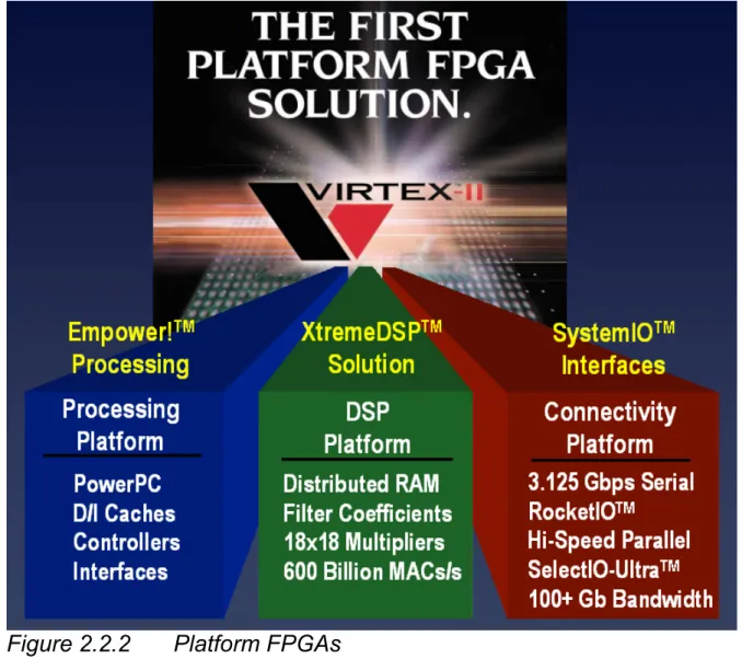
2.2.1 Platform FPGAs Virtex-II™ FPGAs
‘The Platform for Programmable Logic’
The Virtex-II solution is the first embodiment of the Platform FPGA, once again setting a new benchmark in performance, and offering a feature set that is unparalleled in the industry.
It's an era where Xilinx leads the way, strengthened by our strategic alliances with IBM, Wind River Systems, Conexant, RocketChips, The MathWorks, and other technology leaders.
The Platform FPGA delivers SystemIO™ interfaces to bridge emerging standards, XtremeDSP™ for unprecedented DSP performance (up to 100 times faster than the leading DSP processor), and will offer
Empower!™ processor technology for flexible high-performance system processing needs.
The Virtex-II solution is the first embodiment of the Platform FPGA, once again setting a new benchmark in performance, and offering a feature set that is unparalleled in the industry.
With densities ranging from 40,000 up to 10 million system gates, the Virtex-II solution delivers enhanced system memory and lightning –fast DSP through a flexible IP-Immersion fabric.
Additionally, significant new capabilities address system-level design issues including flexible system interfaces with signal integrity
(SystemIO™ , DCI), complex system clock management (Digital Clock Manager), and on-board EMI management (EMIControl™ ).
Virtex-II solutions are empowered by advanced design tools that drive time to market advantages through fast design, powerful synthesis, smart implementation algorithms, and efficient verification capabilities. Not only does the fabric provide the ability to integrate a variety of soft IP, but it also has the capability of embedding hard IP cores such as processors and Gigabit serial I/Os in future Virtex-II families.
Virtex-II Pro™ FPGAs
‘The Platform for Programmable Systems’
With up to four IBM PowerPC™ 405 processors immersed into the industry's leading FPGA fabric, Xilinx/Conexant's flawless high-speed serial I/O technology, and Wind River System's cutting-edge
embedded design tools, Xilinx delivers a complete development
platform of infinite possibilities. The era of the programmable system is here.
The Power of Xtreme Processing
Each PowerPC runs at 300+ MHz delivering 420 Dhrystone MIPS, and is supported by IBM CoreConnect™ bus technology. With the unique Xilinx IP-Immersion architecture, system architects can now harness the power of high-performance processors, along with easy integration of soft IP into the industry's highest performance programmable logic.
XtremeDSP - The World's Fastest Programmable DSP Solution
The Xilinx XtremeDSP solution is the world's fastest programmable DSP solution. With up to 556 embedded 18 x 18 multipliers, 10 Mbits of embedded block RAM, an extensive library of DSP algorithms and tools that include System Generator for DSP, ISE and Cadence SPW, XtremeDSP is the industry's premier programmable solution for
enabling TeraMAC/s applications.
The Ultimate Connectivity Platform
The first programmable device to combine embedded processors along with 3.125 Gbps transceivers, the Virtex-II Pro series addresses all existing connectivity requirements as well as the emerging high-speed interface standards. Xilinx Rocket I/O™ transceivers offer a complete serial interface solution, supporting 10 Gigabit Ethernet with XAUI, 3GIO, SerialATA, you name it. And our SelectI/O™-Ultra
supports 840 Mbps LVDS and high speed single-ended standards such as XSBI and SFI-4.
The Power of Integration
In a single off-the-shelf programmable device, systems architects can take advantage of microprocessors, the highest density of on-chip memory, multi-gigabit serial transceivers, digital clock managers, on-chip termination and more. The result is a dramatic simplification of board layout, a reduced bill of materials, and unbeatable time to market.
Enabling a New Development Paradigm
For the first time ever, systems designers can partition and repartition their systems between hardware and software at any time during the development cycle - even after the product shipped. That means you can optimize the overall system, guaranteeing your performance target in the most cost-efficient manner. You can also debug hardware and software simultaneously at speed.
Industry-Leading Tools
Optimized for the PowerPC, Wind River's industry-proven embedded tools are the premier support for real-time microprocessor and logic designs. Driving the Virtex-II Pro FPGA is the Xilinx lightning-fast ISE software, the most comprehensive, easy-to-use development system available.
2.2.2 Virtex FPGAs
The Xilinx Virtex™ series was the first line of FPGAs to offer one million system gates. Introduced in 1998, the Virtex product line fundamentally redefined programmable logic by expanding the
traditional capabilities of field programmable gate arrays (FPGAs) to include a powerful set of features that address board level problems for high performance system designs.
The latest devices in the Virtex-E series, unveiled in 1999, offer more than three million system gates. The Virtex-EM devices, introduced in 2000 and the first FPGAs to be manufactured using an advanced copper process, offer additional on chip memory for network switch applications.
2.2.3 Spartan FPGAs
Xilinx Spartan™ FPGAs are ideal for low-cost, high volume
applications and are targeted as replacements for fixed-logic Gate Arrays and for application specific standard products (ASSP) products such as bus interface chip sets. The are five members of the family Spartan-3 (1.2V), Spartan IIE (1.8V), Spartan II (2.5V), Spartan XL (3.3V) and Spartan (5V) devices.
The Spartan-3 (1.2V, 90nm) FPGA has been designed to not only be very low cost but integrates many architectural features associated with high-end programmable logic. This combination of low cost and features makes it an ideal replacement for ASICs (Gate Arrays) and many ASSP devices. For example in a Car Multimedia System the Spartan 3 could absorb many system functions. These functions can take the form of embedded IP Cores, bespoke system interfaces, DSP and logic. The diagram below shows such a system:
Figure 2.2.3 Car Multimedia System
In the Car Multimedia System shown in figure 2.2.3 the PCI Bridge takes the form of a pre-verified drop in IP Core, the device level and
board level clocking functions are implemented in the Spartan 3 on-chip Digital Control Management (DCMs). CAN core IP can be used to connect to the body electronics modules, these cores can be provided by AllianceCore partners such as Bosch, Memec Design, Cast, Xylon and Intelliga. On-chip 18x18 multipliers can be used in DSP type activity such as filtering and formatting. Other bespoke interfaces to off-chip processors, IDE interface to the drive unit of a DVD player, audio interfaces, memory and LCD can also be implemented.
Additionally the Spartan 3 XCITE Digitally Controlled Impedance technology can reduce EMI and also component count by providing on-chip tuneable impedances to provide line matching without the need for external resistors.
The Spartan-3 family is based on IBM and UMC advanced 90nm, 8-layer metal process technology. Xilinx is using 90nm technology to drive pricing down to under $20* for a one-million-gate FPGA
(approximately 17,000 logic cells), which represents a cost savings up to 80 percent compared to competitive offerings. A smaller die size and 300mm wafers improve device densities and yields, thereby reducing overall production costs. This in turn leads to a more highly integrated, less expensive product that takes up less board space when designed into an end product.
The Spartan™-3 FPGA memory architecture provides the optimal granularity and efficient area utilization.
Shift Register SRL16 blocks
• Each CLB LUT (Look-Up Table) works as a 16-bit fast, compact shift register
• LUTs can be cascaded to build longer shift registers
• Implement pipeline registers and buffers for video, wireless Up to 520 Kb Distributed SelectRAM+™ Memory
• Each LUT works as a single-port or dual-port RAM/ROM
• LUTs can be cascaded to build larger memories
• Applications include flexible memory sizes, FIFOs, and buffers Up to 1.87 Mb Embedded Block RAM
• Up to 104 blocks of synchronous cascadable 18 Kb block RAM
• Each 18 Kb block can be configured as a single/dual-port RAM
• Supports multiple aspect ratios, data-width conversion and parity
• Applications include data caches, deep FIFOs, and buffers Memory Interfaces. Spartan-3 FPGAs enable electrical interfaces such as HSTL and SSTL to connect to popular external memories.
A variety of Spartan™-3 multipliers enable simple arithmetic and math as well advanced DSP functions. Derive over 330 Billion MACs/sec of DSP performance.
• 18x18 embedded multipliers. Up to 104 18 x 18 multipliers, support 18-bit signed or 17-bit unsigned multiplication, which can be cascaded to support wider bits
• Constant coefficient multipliers. On-chip memories and logic cells work hand-in-hand to build compact multipliers with a constant operand
• Logic Cell multipliers. Implement user-preferred algorithms such as Baugh-Wooley, Booth, Wallace tree, and others
Digital Clock Managers (DCMs) deliver sophisticated digital clock management impervious to system jitter, temperature, voltage
variations and other problems typically found with PLLs integrated into FPGAs.
• Flexible frequency generation from 25 MHz to 325 MHz
o 100ps jitter
o Integer multiplication and division parameters
• Quadrature and precision phase shift control
o 0, 90, 180, 270 degrees
o Fine grain control (1/256 clock period) for clock data
synchronization
• Precise 50/50 duty cycle generation
• Temperature compensation
XCITE Digitally Controlled Impedance Technology- A Xilinx Innovation I/O termination is required to maintain signal integrity. With hundreds of I/Os and advanced package technologies, external termination
resistors are no longer viable. It dynamically eliminates drive strength variation due to process, temperature, and voltage fluctuations.
Spartan-3 XCITE DCI Technology Highlights
o Series and parallel termination for single-ended and differential
standards
o Maximum flexibility with support of series and parallel termination
on all I/O banks
o Input, output, bidirectional and differential I/O support o Wide series impedance range
o Popular standard support including LVDS, LVDSEXT, LVCMOS,
LVTTL,SSTL, HSTL, GTL, and GTLP
Spartan-3 Features and Value
Spartan-3 Feature Value FPGA fabric and routing, up to 5,000,000
system gates
Allows for implementation of system level function blocks, high on-chip connectivity and high-throughput
BlockRAM – 18k blocks Enables implementation of large packet buffers/FIFOs, line buffers
Distributed RAM For implementing smaller FIDOs/Buffers, DSP coefficients
Shift register mode (SRL16) 16-bit shift register ideal for capturing high speed or burst mode data and to store data in DSP and encryption applications e.g. fast pipelining
Dedicated 18 x 18 multiplier blocks High speed DSP processing; use of multipliers in conjunction with fabric allows for ultra-fast, parallel DSP operations Single-ended signalling (up to 622 Mbps) –
LVTTL, LVCMOS, GTL, GTL+, PCI, HSTL-I, IHSTL-I, IIHSTL-I, SSTL-HSTL-I,II
Connectivity to commonly used to-chip, memory (SRAM, SDRAM) and chip-to-backplane signalling standards;
eliminates the need for multiple translation ICs
Differential signalling (up to 622 Mbps) - LVDS, BLVDS, Ultra LVD, SRSDS and LDT
Differential signalling at low cost – bandwidth management (saving the number of pins, reduced power
consumption, reduced EMI, high noise immunity
Digital clock management (DCM) Eliminate on-chip & board level clock delay, simultaneous multiply and divide, reduction of board level clock speed and number of board level clocks, adjustable clock phase for ensuring coherency Global routing resources Distribution of clocks and other signals
with very high fanout throughout the device Programmable output drive Improves signal integrity, achieving right
Spartan IIE
The Spartan-IIE (1.8V core) family offers some of the most advanced FPGA technologies available today, including programmable support for multiple I/O standards (including LVDS, LVPECL & HSTL), on-chip block RAM and digital delay lock loops for both chip-level and board-level clock management. In addition, the Spartan-IIE devices provide superior value by eliminating the need for many simple ASSPs such as phase lock loops, FIFOs, I/O translators and system bus drivers that in the past have been necessary to complete a system design.
Spartan-IIE Architectural Features
Figure 2.5 Spartan IIE Architecture
The Spartan-IIE family leverages the basic feature set of the Virtex-E architecture in order to offer outstanding value. The basic CLB
structure contains distributed RAM and performs basic logic functions. The four DLLs are used for clock management and can perform clock de-skew, clock multiplication, and clock division. Clock de-skew can be done on an external (board level) or internal (chip level) basis.
The block memory blocks are 4K bits each and can be configured from 1 to 16 bits wide. Each of the two independent ports can be configured for width independently.
The SelectI/O feature allows many different I/O standards to be implemented in the areas of chip, memory, and chip-to-backplane interfaces
Spartan-IIE Block Diagram
Figure 2.6 Spartan IIE Block Diagram
The Spartan-IIE family of Field Programmable Gate Arrays (FPGAs) is implemented with a regular, flexible, programmable architecture of Configurable Logic Blocks (CLBs), surrounded by a perimeter of programmable Input/Output Blocks (IOBs), interconnected by a
powerful hierarchy of versatile routing resources. The architecture also provides advanced functions such as Block RAM and clock control blocks.
Spartan-IIE Input/Output Block
Figure 2.7 Spartan IIE Input/Output Block
The Spartan-IIE IOB features inputs and outputs that support 19 I/O signalling standards, including LVDS, BLVDS, LVPECL, LVCMOS, HSTL, SSTL, and GTL. These high-speed inputs and outputs are capable of supporting various state-of-the-art memory and bus
interfaces. The three IOB registers function either as edge-triggered D-type flip-flops or as level sensitive latches. Each IOB has a clock signal (CLK) shared by the three registers and independent clock enable (CE) signals for each register.
In addition to the CLK and CE control signals, the three registers share a Set/Reset (SR). For each register, this signal can be independently configured as a synchronous Set, a synchronous Reset, an
Spartan-IIE Banking of I/O Standards
Figure 2.8 Spartan IIE Banking of I/O Standards
Some of the I/O standards require VCCO and/or VREF voltages. These voltages externally are connected to device pins that serve groups of IOBs, called banks. Consequently, restrictions exist about which I/O standards can be combined within a given bank. Eight I/O banks result from separating each edge of the FPGA into two banks. Each bank has multiple VCCO pins, all of which must be connected to the same voltage. This voltage is determined by the output standards in use.
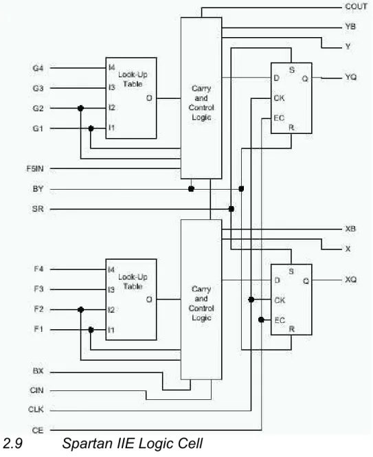
Logic Cells
The basic building block of the Spartan-IIE CLB is the logic cell (LC). An LC includes a four-input function generator, carry logic, and a storage element. The output from the function generator in each LC drives both the CLB output and the D input of the flip-flop. Each
Spartan-IIE CLB contains four LCs, organised in two similar slices. In addition to the four basic LCs, the Spartan-IIE CLB contains logic that combines function generators to provide functions of five or six inputs. Consequently, when estimating the number of system gates provided by a given device, each CLB counts as 4.5 LCs.
Spartan-IIE function generators are implemented as 4-input look-up tables (LUTs). In addition to operating as a function generator, each LUT can provide a 16 x 1-bit synchronous RAM. Furthermore, the two LUTs within a slice can be combined to create a 16 x 2-bit or 32 x 1-bit synchronous RAM, or a 16x1-bit dual-port synchronous RAM. The Spartan-IIE LUT can also provide a 16-bit shift register that is ideal for capturing high-speed or burst-mode data. This SRL16 (Shift Register LUT) mode can be used to increase the effective number of flip-flops by a factor of 16. Adding flip-flops enables fast pipelining which are ideal for DSP applications. The storage elements in the Spartan-IIE slice can be configured either as edge-triggered D-type flip-flops or as level-sensitive latches.
Block RAM
Spartan-IIE FPGAs incorporate several large Block SelectRAM+ memories. These complement the distributed SelectRAM+ resources that provide shallow RAM structures implemented in CLBs. Block SelectRAM+ memory blocks are organised in columns. All Spartan-II devices contain two such columns, one along each vertical edge. These columns extend the full height of the chip. Each memory block is four CLBs high, and consequently, a Spartan-IIE device 8 CLBs high will contain 2 memory blocks per column, and a total of 4 blocks.
Figure 2.11 Block RAM Applications
Delay-Locked Loop
Associated with each global clock input buffer is a fully digital Delay-Locked Loop (DLL) that can eliminate skew between the clock input pad and internal clock input pins throughout the device. Each DLL can drive two global clock networks. The DLL monitors the input clock and the distributed clock, and automatically adjusts a clock delay element. Additional delay is introduced such that clock edges reach internal flip-flops exactly one clock period after they arrive at the input. This closed-loop system effectively eliminates clock-distribution delay by ensuring that clock edges arrive at internal flip-flops in synchronism with clock edges arriving at the input.
Figure 2.12 Spartan IIE Clock Management
Configuration
Configuration is the process by which the FPGA is programmed with the configuration file generated by the Xilinx development system. Spartan-IIE devices support both serial configuration, using the master/slave serial and JTAG modes, as well as byte-wide configuration employing the slave parallel mode.
Figure 2.14 Spartan IIE Family Overview
Xilinx CPLDs
Currently, Xilinx offers CPLD products in two categories: XC9500 and CoolRunner. To choose a CPLD that's right for you, review the product features below to identify the product family that fits your application, then review the selection considerations to choose the device that best meets your design criteria.
Product Features:
XC9500 - The XC9500 In-System Programmable (ISP) CPLD families take complex programmable logic devices to new heights of high-performance, feature-richness, and flexibility. These families deliver industry-leading speeds, while giving you the flexibility of enhanced customer proven pin-locking architecture along with extensive IEEE Std.1149.1 JTAG boundary scan support. This CPLD family is ideal for high speed, low cost designs.
CoolRunner - The CoolRunner product families offer extreme low power making them the leaders in an all new market segment for CPLDs - portable electronics. With standby current in the low micro amps and minimal operational power consumption, these parts are ideal for any application is that is especially power sensitive, for example, battery powered or portable applications. CoolRunner II extends the CPLD usage as it offers system level features such as LVTTL & SSTL, Clocking modes and input hysteresis.
Selection Considerations:
To decide which device best meets your design criteria, take a minute to jot down your design specs (using the list below as a criteria reference). Next, go to a specific product family page to get more detailed information about the device you need.
Density - for each part, an equivalent 'gate count' is given. This is an estimate of the logic density of the part.
Number of registers - count up the number of registers you need for your counters, state machines, registers and latches. The number of macrocells in the device must be at least this large.
Number of I/O pins - How many inputs and outputs does your design need?
Speed requirements - What is the fastest combinatorial path in your design? This will determine the tpd (propagation delay through the device in nano seconds) of the device. What is the fastest sequential circuit in your design? This will tell you what fMax (Maximum
frequency) you need.
Package - What electromechanical constraints are you under? Do you need the smallest ball grid array package possible or can you use a more ordinary QFP? Or are you prototyping and wish to use a
socketed device, in this case a PLCC package?
Low Power - is your end product battery or solar powered? Does your design require the lowest power devices possible? Do you have heat dissipation concerns?
System Level Functions - Does you board have multi-voltage devices? Do you need to level shift between these devices? Do you need to square up clock edges? Do you need to interface to memories and microprocessors?
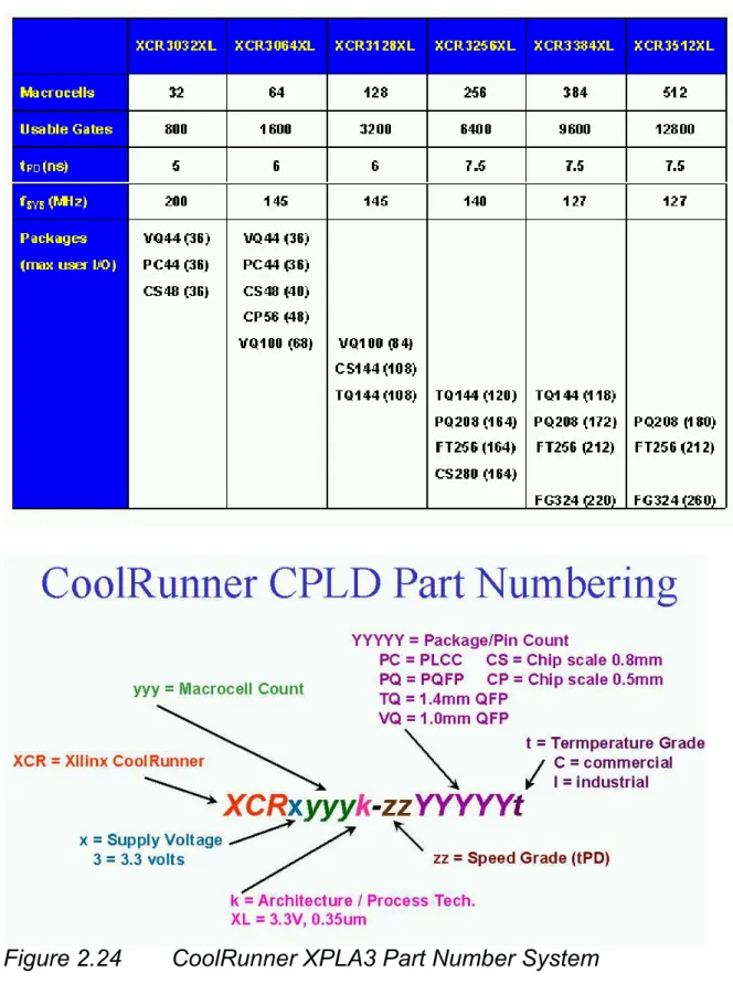
XC9500 ISP CPLD Overview
The high-performance, low-cost XC9500™ families of Xilinx CPLDs are targeted for leading-edge systems that require rapid design development, longer system life, and robust field upgrade capability. The XC9500 families range in density from 36 to 288 macrocells and are available in 2.5-volt (XC9500XV), 3.3-volt (XC9500XL) and 5-volt (XC9500) versions. These devices support In-System Programming (ISP) which allows manufacturers to perform unlimited design
iterations during the prototyping phase, extensive system in-board debugging, program and test during manufacturing, as well as field upgrades. Based upon advanced process technologies, the XC9500 families provide fast, guaranteed timing, superior pin locking, and a full JTAG compliant interface. All XC9500 devices have excellent quality and reliability characteristics with 10,000 program/erase cycles
XC9500 5V Family
The XC9500™ In-System Programmable (ISP) CPLD family takes complex programmable logic devices to new heights of
high-performance, feature-richness, and flexibility. This 5V family delivers industry-leading speeds, while giving you the flexibility of an enhanced customer proven pin-locking architecture along with extensive IEEE Std. 1149.1 JTAG boundary scan support. It features six devices ranging from 36 to 288 macrocells with a wide variety of package combinations that both minimise board space and maintain package footprints as designs grow or shrink. All I/O pins allow direct
interfacing to both 3 and 5 volt systems, while the latest in compact, easy-to-use CSP and BGA packaging gives you access to as many as 192 signals.
Flexible Pin-Locking Architecture
The XC9500 devices, in conjunction with our fitter software, give you the maximum in routeability and flexibility while maintaining high performance. The architecture is feature rich, including individual p-term output enables, three global clocks, and more p-p-terms per output than any other CPLD. The proven ability of the architecture to adapt to design changes while maintaining pin assignments (pin-locking) has been demonstrated in countless real-world customer designs since the introduction of the XC9500 family. This assured
pin-locking means you can take full advantage of
in-system-programmability and you can easily change at any time, even in the field.
Full IEEE 1149.1 JTAG Development and Debugging Support
The JTAG capability of the XC9500 family is the most comprehensive of any CPLD on the market. It features the standard support including BYPASS, SAMPLE/PRELOAD, and EXTEST. Additional boundary scan instructions, not found in any other CPLD, such as INTEST (for device functional test), HIGHZ (for bypass), and USERCODE (for program tracking), allow you the maximum debugging capability. The XC9500 family is supported by a wide variety of industry standard third-party development and debugging tools including Corelis, JTAG Technologies, and Asset Intertech. These tools allow you to develop boundary scan test vectors to interactively analyse, test, and debug system failures. The family is also supported on all major ATE
platforms including Teradyne, Hewlett Packard, and Genrad.