Springer-Verlag, Vol. 23, No 1, pp. 77-100, 2005.
Open Mobile Alliance (OMA) Security Layer: Architecture,
Implementation and Performance Evaluation of the Integrity Unit
N. Sklavos, P. Kitsos, E. Alexopoulos and O. Koufopavlou Electrical and Computer Engineering Department
University of Patras, Patras GREECE [email protected]
Abstract:
Security has become a very critical issue in the provision of mobile services. The Open Mobile Alliance (OMA) has specified a powerful security layer, the WTLS. In this paper, a VLSI architecture for the implementation of the WTLS integrity unit is proposed. The proposed architecture is reconfigurable in the sense that operates in three different modes: as Keyed-Hash Authentication Code (HMAC), as SHA-1 and MD5 hash functions, according to WTLS specifications. This multi-mode operation is achieved due to the reconfigurable applied design technique in the proposed architecture, which keeps the allocated area resources at a minimized level. The proposed architecture achieves high speed performance, due to the pipeline designed architecture. Especially, SHA-1 operation achieved throughput is equal to 1,7 Gbps, while MD5 operation mode bit rate is equal to 2,1 Gbps. The proposed architecture has been integrated by using VHDL and has been synthesized placed and routed in an FPGA device. Comparisons with related hash functions implementations have been done in terms of throughput, operating frequency, allocated area and Area-Delay product. The achieved performance of the SHA-1 operation mode is better at about 14-42 times compared with the other conventional works. In addition, MD5 performance is superior to the other works at about 6-18 times, in all of the cases. The proposed Integrity Unit is a very trustful and powerful solution for the WTLS layer. In addition, it can be integrated in security systems which are used for the implementation networks for wireless protocols, with special needs of integrity in data transmission.
Keywords: Open Mobile Alliance, Wireless Application Protocol, Hardware Implementation,
Springer-Verlag, Vol. 23, No 1, pp. 77-100, 2005.
1. INTRODUCTION
The Open Mobile Alliance is completely a new concept. It is specified by a consortium, the OMA Forum, in June 2002 [1]. The mission of the Open Mobile Alliance is to grow the market for the entire mobile industry by removing the barriers to global user adoption, and by ensuring seamless application interoperability, while allowing businesses to compete through innovation and differentiation. Wireless networks intentionally radiate data over the area, which could be allocated and outside of the limits that the network controls. This means that someone can passively retrieve all the transmitted information from a distance with the appropriate technical equipment. It is obvious that wireless communications as a shared medium could be easily intercepted. Bulk encryption, integrity and authentication are always considered when developing a wireless standard, such as OMA, or a mobile networking system. Especially integrity is a very critical security issue in addition to the encryption of data transmission [2-3]. Every client and application server provider must be authenticated, in order both communication parties to be safely sure, that the other part is the original one that it claims to be. In most of the cases, the services need strong authentication with certificates. Especially, OMA has specified a powerful security layer, the Wireless Transport Layer Security (WTLS).
In this paper, a VLSI architecture for the implementation of the WTLS Integrity Unit is proposed. The proposed architecture performs efficiently for three different operation modes: as original SHA-1 and MD5 hash functions [2-3], and as Keyed-Hash Message Authentication Code (HMAC) [4], according to WTLS specifications. The HMAC operation mode is based on the hash computations of the input data, alternatively by using one of the two specified hash functions (MD5 and SHA-1). The operation mode is selected upon to the user’s needs each time, and it is not predefined by the proposed Integrity Unit operation scenario. This multi-mode operation is achieved by a reconfigurable hash function core, which minimizes the allocated area resources and achieves high speed performance.
The proposed architecture has been developed by using the VHDL description language, and has been synthesized placed and routed in an FPGA device. From the synthesis results it is proven that the introduced Integrity Unit has ultra high speed performance. Especially, the achieved throughput is equal to 1,7 Gbps for the SHA-1 hash function. In the case of MD5 operation system performance is equal to 2,1 Gbps. When the Integrity Unit operates as HMAC security scheme, the system performance is equal to the throughput of the selected hash function (MD5, or SHA-1) each time. Comparisons with related hash functions implementations have been done in terms of throughput, operating frequency, allocated area and Area-Delay product. The achieved performance of the SHA-1 operation mode is better at about 1428-4250 % compared with the other conventional architectures. In addition, the MD5 operation performance is superior to the other related works at about 600-1800 %. These performance results have been achieved due to the applied pipeline methodology in the Integrity Unit architecture. In addition with the reconfigurable architecture design the allocated area resources are kept at a minimized level. The above advantages prove that the proposed unit is a very trustful and powerful solution for the WTLS layer. Furthermore, this Integrity Unit can be used hash functions applications of all the types, with hard high-speed performance demands (LANs, Wireless Protocols), and with high-level security needs for data integrity, at the same time.
This paper is organized as follows: in section two the WTLS layer is described. In the next section, the proposed Integrity Unit architecture is presented in detail. Section 4 is dedicated to the system evaluation and testing. The VLSI implementation results are given in the section 5 and comparisons with other related works are presented. Finally, conclusions and observations are discussed in the last section.
Springer-Verlag, Vol. 23, No 1, pp. 77-100, 2005.
2. SECURITY AND WIRELESS TRANSPORT LAYER SECURITY (WTLS)
Security is very critical issue in wireless communications and especially in OMA, in order the users safely and honestly to connect in sensitive services, such as e-commerce and online-banking. The security layer of OMA is the Wireless Transport Layer (WTLS) [5]. It is the equivalent to the Transport Security Layer (TLS) in the mobile world [6]. WTLS introduces new features such as key refreshing, datagram support, optimized packet size and handshake. The data transmission in WTLS is supported by the security schemes of privacy, message integrity and authentication. The privacy is based on DES, IDEA, and RC5 ciphers, while for integrity MD5 and SHA-1 hash functions have been specified. In authentication, RSA, Diffie-Hellman and Elliptic Curve algorithms have been selected. In addition, specialized security mechanisms such as HMAC and Digital Signature have been adopted by OMA, in order to support powerfully the WTLS layer.
The Data Integrity Unit of WTLS is based on two powerful and widely used hash functions: SHA-1 and MD5. Hash functions are used for digital signature scheme, data integrity, HMAC and other cryptographic purposes (random number generators) [2-3, 7-8]. These functions map data messages of an arbitrary length, to a hash value of fixed length. This last value is called message digest.
MD5 is the hash function developed by Ronald Rivest [9]. The algorithm accesses 512-bit message blocks and finally produces a 128-bit message digest. This hash function is an improved version of MD4 but a more complex design [2-3, 7]. In MD5 architecture a fourth round has been added, while each transformation step has a unique additive constant. Each step now adds the result of the previous transformation step. This promotes a faster avalanche effect compared with MD4. Furthermore the order of the processed message sub-blocks is changed in transformation rounds 2 and 3. In spite of these differences, both MD4 and MD5 produce a 128-bit.
SHA-1 is the Secure Hash Algorithm designed by NIST [10]. This hash function is widely used in the Digital Signature Algorithm. SHA-1 is based on design aspects and mathematical principles similar to MD4 and MD5. Especially, SHA-1 has almost the same architecture as MD4 with the addition of an expand transformation, an extra round, and with better avalanche effect [2-3, 7]. SHA-1 produces a 160-bit message digest, longer than the generated 128-bit of MD5. SHA-1 offers high security level, and no cryptanalytic attack has been applied successfully against this hash function. The 160-bit message digest of SHA-1 makes it more resistant to birthday and brute-force-attacks than the 128-bit hash value of MD5.
Both MD5 and SHA-1 support efficiently the Hash Message Authentication Code (HMAC). On April 3, 2002, it was announced the FIPS-198, The Keyed-Hash Message Authentication Code (HMAC) and this publication became a Federal Standard on March 6, 2002 [4]. This standard specifies a mechanism for message authentication using cryptographic hash functions. HMAC can be used with any iterative FIPS approved hash function, in combination with a shared secret key.
According to HMAC standard, SHA-1 and MD5 hash functions can be used alternatively, in order to support its operation. HMAC has defined two functional distinct parameters, the input data message and the secret key. We assume K the secret key and H(x) the used hash function. The input message is hashed by iterating a basic compression function on blocks of data (512-bit for both SHA-1 and MD5). With B=64 is denoted the byte-length of such blocks and is L the byte-length of the hash function output (with L=16 for MD5 and L=20 for SHA-1). The authentication key can be of any length up to B, which is the length of the hash function input data block. In applications that keys with longer length than B are required, the key is firstly hashed by using the H(x) function. Then the resultant L bytes data block (hash function output) is used, as the actual key to HMAC. In any case, the minimal recommended length for K is L bytes. In addition two fixed constants are specified: ipad, which is equal to the byte “36” repeated B times for the inner, and opad, which is equal to the byte “5C” repeated B times for the outer. In order to compute the HMAC over a data block, the following defined function is used:
Springer-Verlag, Vol. 23, No 1, pp. 77-100, 2005.
HMAC(K,D)=H{(K XOR opad) || H (K XOR ipad || D)} (I) where: || indicates concatenation.
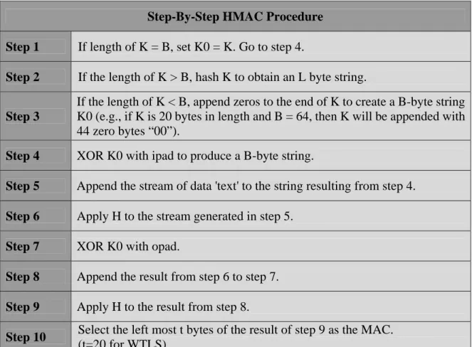
In the above equation, the block K indicates the HMAC key and D is the input data block. In this equation XOR block has higher precedence than concatenation ||. In the following Table 1 the HMAC scheme is presented in detail (step-by-step described procedure).
Step-By-Step HMAC Procedure
Step 1 If length of K = B, set K0 = K. Go to step 4.
Step 2 If the length of K > B, hash K to obtain an L byte string.
Step 3
If the length of K < B, append zeros to the end of K to create a B-byte string K0 (e.g., if K is 20 bytes in length and B = 64, then K will be appended with 44 zero bytes “00”).
Step 4 XOR K0 with ipad to produce a B-byte string.
Step 5 Append the stream of data 'text' to the string resulting from step 4.
Step 6 Apply H to the stream generated in step 5.
Step 7 XOR K0 with opad.
Step 8 Append the result from step 6 to step 7.
Step 9 Apply H to the result from step 8.
Step 10 Select the left most t bytes of the result of step 9 as the MAC.
(t=20 for WTLS)
Table 1: HMAC Scheme Procedure
Furthermore, in the Appendix the most important technical issues of both SHA-1 and MD5 standards are presented. The Appendix is a brief presentation of the standard specifications [9,10] and it is given for better understanding. Due to the limited length of the paper, used constants, generation constants mechanisms, analytical arithmetic and logical functions and padding operations are not included. For more information about the SHA-1 and MD5 hash family the readers are encouraged to study the standard specifications [9,10].
3. PROPOSED INTEGRITY UNIT ARCHITECTURE
3.1 Proposed Architecture
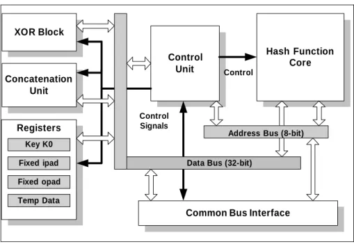
The proposed architecture for the implementation of WTLS Integrity Unit is illustrated in the following Figure 1.
Springer-Verlag, Vol. 23, No 1, pp. 77-100, 2005. Control Unit Hash Function Core Concatenation Unit
Common Bus Interface XOR Block
Registers
Data Bus (32-bit)
Address Bus (8-bit) Key K0 Fixed ipad Fixed opad Temp Data Control Signals Control
Figure 1: Proposed Integrity Unit Architecture
The heart of the Integrity Unit is the Hash Function Core, which implements both SHA-1 and MD5 hash functions. Especially this core operates efficiently in two different modes, one for each hash function, and will be analyzed in detail in the next sections. Like the most of the system-on-chip designs the above proposed architecture includes a simple Common Bus Interface unit for communication with the external environment. Two internal buses, the address and the data bus of 8- and 32-bit respectively, have also been integrated. In addition, an XOR block and a Concatenation Unit have also been included in the proposed Integrity Unit architecture. The Concatenation Unit is necessary for all the needed appending data processes. Finally, four registers are used for the specified constants, key and temporary data storage.
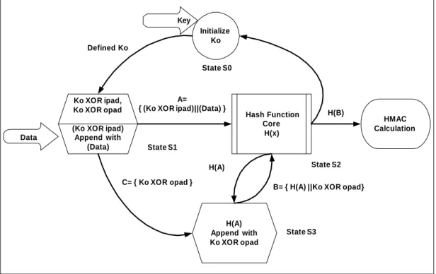
The proposed Integrity Unit is reconfigurable in the sense that operates for three different modes: for SHA-1 and MD5 hash functions, and for HMAC security scheme. The selection of the operation mode is upon to the user needs it’s time, and it is not predefined by the Integrity Unit operation scenario. Especially, in the case of HMAC operation mode, the Control Unit coordinates all the system’s operations, according to an FSM (Finite State Machine) diagram which is shown in the next Figure. 2.
This FSM diagram is based on the specified HMAC step-by-step procedure, which has been described in the previous Table I. In the State S0, the used key Ko is initialized (entered by the user). Then the procedure is continued to the State S1. As the Figure 2 shows, in this state, some XOR transformations are performed between the key Ko, and the constants ipad and opad. The input data are concatenated to the end of the generated data block {Ko XOR ipad} and in this way the data output A is generated. The State S2 includes the Hash Function Transformation of the data block A. This transformation is based on MD5 or SHA-1 hash function. The selection of the used hash it’s time is upon to the user demands. Then, the HMAC operation is continued to the State S3. As the Figure 2 indicates, the produced data block B is equal to the concatenation of the hash value H(A) with the produced C data block of the State S1. After the B data block generation, the operation returns to State S2. The produced new hash value H(B) of this State, is the requested hash value (HMAC calculation). Then, the system returns to the initial State S0. The system remains in this state (idle mode) until the next HMAC calculation is requested. The produced HMAC calculation is equal to 128-bit when MD5 is selected and equal to 160-bit in the case of SHA-1 operation.
Except the HMAC operation mode, the proposed Integrity Unit architecture operates efficiently as an original MD5 or SHA-1 hash function, according to WTLS specifications. When the user demands
Springer-Verlag, Vol. 23, No 1, pp. 77-100, 2005.
the proposed reconfigurable architecture (Figure 1) to operate as MD5 or SHA-1, the Control Unit uses only the Hash Function Core and not any other unit, in order to perform the requested task, as an original MD5 or SHA-1 hash function.
Initialize Ko
Ko XOR ipad, Ko XOR opad (Ko XOR ipad)
Append with (Data) H(A) Append with Ko XOR opad Hash Function Core H(x) HMAC Calculation H(A) A=
{ (Ko XOR ipad)||(Data) }
B= { H(A) ||Ko XOR opad} H(B) Key Data C= { Ko XOR opad } Defined Ko State S0 State S1 State S3 State S2
Figure 2: HMAC Operation Mode FSM Diagram
3.2 Hash Function Core
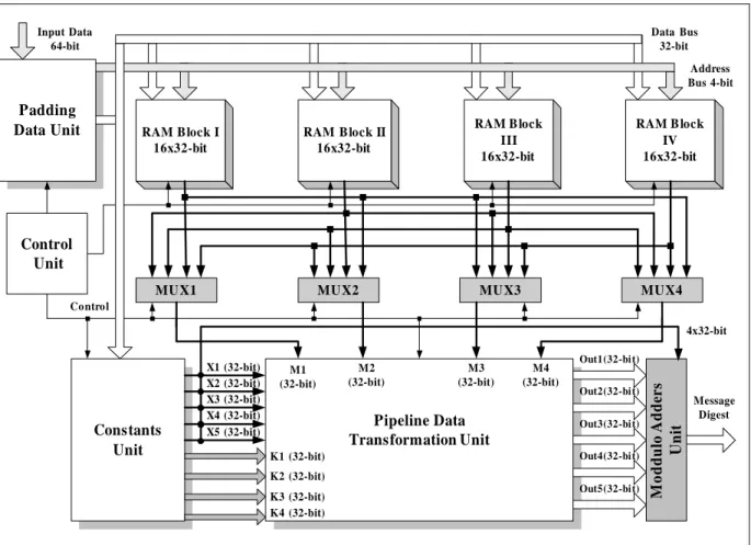
The critical component of the Integrity Unit (Figure 1) is the Hash Function Core. The architecture of this component is illustrated in the next Figure 3. The Hash Function Core, as it has already been mentioned before, operates for both MD5 and SHA-1 hash functions, alternatively.
The Padding Data Unit pads the input data and converts them to 512-bit blocks (padded data). This procedure is the same for both hash functions. It is characterized of simplicity and it is well defined by both MD5 and SHA-1 specifications [16], [17]. The purpose of padding is to make the total length of an input message a multiple of 512-bit. Both hash functions sequentially process blocks of 512-bit, when they compute the message digest. The padded data are generated according to the following process: a logic “1”, followed by m “0”s, followed by a 64-bit integer are appended to the end of the input data, to produce a padded data block with length equal to 512*n. The 64-bit integer is equal to the length of the input data message. The next Table II shows the structure of the padded data block.
Input Data
Message “1” “000…000” 64-bit Integer
512 66+m 65+m 64+m 65 64 1 Padded Data Block 512-bit
Springer-Verlag, Vol. 23, No 1, pp. 77-100, 2005.
Every produced Padded Data Block is stored in one of the four used RAM Blocks (Figure 3). Four Padded Data Blocks in total can be processed by the Hash Function Core at the same time. The appropriate data transformation is performed in the Pipeline Data Transformation Unit. The specified constants, for the MD5 and SHA-1 operations, are stored in the Constants Unit. The transformed data are finally modified by the Modulo Adders Unit, and in this way the message digest is produced.
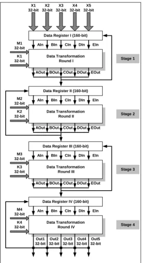
The Pipeline Data Transformation Unit is the critical component for the data transformation of the Hash Function Core. The architecture of this unit is shown in Figure 4 and has been designed with pipeline applied technique. Especially, this unit consists of four different data transformation rounds. Of course, the pipeline applied design technique demands four registers, one for each data transformation round. Every round operates on 5 inputs (AIn, BIn, CIn, Din, EIn) plus the message input (Mi) and the constant input (Ki), all equal to 32-bit.
RAM Block I 16x32-bit Address Bus 4-bit RAM B lock II 16x32-bit RAM B lock III 16x32-bit RAM B lock IV 16x32-bit MU X1 MU X2 MU X3 MU X4 Out1 (32-bi t) Pipeline Data Transformation Unit M o ddul o Adde rs Uni t M1 (32-bit) M2 (32-bit) M3 (32-bit) M4 (32-bit) Message Digest Data Bus 32-bit Padding Data Unit Constants Unit Control Unit Input Data 64-bit X2 (32-bit) X3 (32-bit) X4 (32-bit) X1 (32-bit) K2 (32-bit) K3 (32-bit) K4 (32-bit) K1 (32-bit) 4x32-bit Control X5 (32-bit) Out2 (32-bi t) Out3 (32-bi t) Out4 (32-bi t) Out5 (32-bi t)
Figure 3: Hash Function Core Architecture
In the case of the MD5 operation the Pipeline Data Transformation Unit uses only the four inputs/outputs (B,C,D,E) of each one of the four Data Transformation Rounds. The input/output named A is not used (idle), for this hash function operation (MD5). This is due to the fact that MD5 processes on 128-bit blocks (4x32-bit) transformation blocks, instead of the 160-bit blocks (5x32-bit) that are used in SHA-1. The specified constants for the MD5 operation are stored in the Constants Unit. Four 32-bit constants (initial values) have been defined. These values (X1, X2, X3, X4) are called chaining variables. In addition, every one of the four data Transformation Rounds demands 16x32-bit constants, (K1, K2, K3, K4). The four Data Transformation Rounds are similar, but its one performs a different operation. In Figure 5, the integrated architecture for the Data Transformation Rounds is presented in detail.
Springer-Verlag, Vol. 23, No 1, pp. 77-100, 2005.
Data Transformation Round I Data Register I (160-bit) X1 32-bit X2 32-bit X3 32-bit X4 32-bit X5 32-bit
AIn BIn CIn DIn EIn
AOut BOut COut DOut EOut M1 32-bit K1 32-bit Data Transformation Round II Data Register II (160-bit)
AIn BIn CIn DIn EIn
AOut BOut COut DOut EOut M2 32-bit K2 32-bit Data Transformation Round III Data Register III (160-bit)
AIn BIn CIn DIn EIn
AOut BOut COut DOut EOut M3 32-bit K3 32-bit Data Transformation Round IV Data Register IV (160-bit)
AIn BIn CIn DIn EIn
Out1 32-bit Out2 32-bit Out3 32-bit Out4 32-bit Out5 32-bit M4 32-bit K4 32-bit Stage 1 Stage 2 Stage 3 Stage 4
Figure 4: Pipeline Data Transformation Unit
Ki 32-bit MA MA MA Shifter <<< MA Nonlinear Function i Shifter <<< Shifter <<< Mux Mux Mi 32-bit Ein 32-bit Din 32-bit Cin 32-bit Bin 32-bit Ain 32-bit M U L T I P L E X E R EOut 32-bit DOut 32-bit COut 32-bit BOut 32-bit AOut 32-bit AND AND OR Not AND AND OR Not X O R MUX X Y Z F1Out
NF1(x,y,z) NF2(x,y,z) F2Out
X Z Y MD5 SHA-1 XOR OR Not X O R MUX NF4(x,y,z) F4Out Y Z X MD5 SHA-1 AND AND OR X O R MUX NF3(x,y,z) F3Out X Y Z SHA-1 MD5 AND (A ) D a ta T ra n s fo rma ti on R o un d i (B) No nl inear Fun ctio ns i N F 1, NF 2, NF 3, NF4
Springer-Verlag, Vol. 23, No 1, pp. 77-100, 2005.
In the above architecture the MA components indicate modulo addition 232, while the shifters components define left shift rotations of the input data block. The Data Transformation Round i operation is based on a Nonlinear Function i transformation of the three of BIn, CIn, and DIn, inputs. Then, this result is added to the fourth input EIn with the input data block (Mi) and the constant (Ki). That result is rotated to the right and the rotated output data are added with the input DIn. There are four different nonlinear functions, one used for each Data Transformation Round, which perform the digital logic transformation according to the following equations:
MD5 Round Block 1: F1 (X,Y,Z)= ( X AND Y ) OR [ ( NOT X ) AND Z ] (II) MD5 Round Block 2: F2 (X,Y,Z)= ( X AND Z ) OR [ Y AND ( NOT Z ) ] (III) MD5 Round Block 3: F3 (X,Y,Z)= ( X XOR Y XOR Z ) (IV) MD5 Round Block 4: F4 (X,Y,Z)= Y XOR [ X OR ( NOT Z ) ] (V) where X,Y,X are 32-bit variables.
In the proposed architecture of Figure 3, four different padded data blocks are been processed at the same time. When the transformation of the N padded data block is completed in the Data Transformation Round K, then it is forwarded to round K+1. After that, the N+1 padded data block is forced to the K data Transformation Round Block. This operation is repeated every 16 clock cycles. Every padded data block needs 64 clock cycles in total to be completely transformed, in the four Data Transformation Rounds.
The Hash Function Core (Figure 3) can be used alternatively for the operation SHA-1 hash function also. In this case, the Pipeline Data Transformation Unit and the Data Transformation Rounds process the data in a different way, compared with MD5 operation mode, in order the Hash Function Core to perform efficiently as SHA-1 hash function.
For the SHA-1 operation each Data Transformation Round operates on all the five 32-bit variables (inputs/outputs) and this is one of the basic differences compared with MD5 mode. Especially each output of the Data Transformation Round is equal to critical data path transformation of the following equations:
AOut = {Left Circular Shift (BIn), by 5-bit} + Fi (Bin, CIn, DIn) + EIn + Wi + Ki (VI) Bout = AIn (VII) COut = {Left Circular Shift (BIn), by 30-bit} (VIII) DOut = CIn (IX) EOut = DIn (X) The Nonlinear Function Fi, of each Data Transformation Round performs a different digital logic transformation this time. The next four equations define the Nonlinear Functions operation in each case (Transformation Round):
SHA-1 Round 1: F1 (X,Y,Z)= ( X AND Y ) OR [ ( NOT X ) AND Z ] (XI) SHA-1 Round 2: F2 (X,Y,Z)= ( X XOR Y XOR Z ) (XII) SHA-1 Round 3: F3 (X,Y,Z)= (X AND Y) OR (X AND Z) OR (Z AND Y) (XIII) SHA-1 Round 4: F4 (X,Y,Z)= ( X XOR Y XOR Z ) (XIV) where X,Y,X are 32-bit variables.
In addition four 32-bit constants are used (K1, K2, K3, K4), one for each round of the Pipeline Data Transformation Unit. It has to be mentioned that both initial values and rounds constants have been specified by SHA-1 standard [10]. Especially, the initial values are refreshed each time, a new message digest is produced (for more details see [10]). The data are transformed 20 times in each round (80 times in total) and finally a 160-bit (5x32-bit) transformed data block is produced. The
Springer-Verlag, Vol. 23, No 1, pp. 77-100, 2005.
Constants Unit (Figure 3) in the case of SHA-1 operation initializes the inputs of Pipeline Data Transformation Unit, with five 32-bit different initial values, compared with MD5 mode.
The design criteria of both Pipeline Data Transformation (Figure 4) and Data Transformation Round i (Figure 5) units have been derived as a combination of both MD5 and SHA-1 standards specifications (see [9], [10] and Appendix). Both hash functions use four basic iterations of data transformations (according to four equations, (II)-(V) for MD5 and (XI)-(XIV) for SHA-1). For each iteration loop, which executes the calculation of an equation for many times, a pipeline stage has been designed. So, totally there are four stages (Figure 4). Each one of the equations, (II)-(V) for MD5, and (XI)-(XIV) for SHA-1, is calculated by the Data Transformation Round i. The Nonlinear Function i (Figure 5), operates in two different modes, one for MD-5 and one for SHA-1. Especially, NF1 operates in one common mode for both MD5 and SHA-1, since equations (II) for MD5 is equal to equation (XI) for SHA-1. NF2 function calculates equation (III) for MD5, and (VII) for SHA-1. NF3 function calculates equation (IV) for MD5 and (VIII) for SHA-1. Finally, NF4 function calculates equation (V) for MD5 and (IX) for SHA-1. The operation of each Data Transformation Round i is supported by 16X32 constants, which are stored in four RAM Block sets (Figure 3), one block per round.
The Pipeline Data Transformation Round generates a data block equal to 160-bit (5x32) and 128-bit (4x32) for SHA-1 and MD5 operation modes respectively. This block is forced to the Modulo Adder Unit (Figure 3). The Modulo Adders Unit consists of 5 modulo adders. In this unit modulo additions 232 are performed, between the input data (Out1, Out2, Out3, Out4, Out5) and the constants (X1, X2, X3, X4, X5). In this way, the message digest is finally produced. In the case of MD5 operation, only the four data blocks are processed (Out2, Out3, Out4, Out5) and a 128-bit (4x32-bit) message digest is produced. In the case of SHA-1 operation all the five data blocks are transformed by the Modulo Adders Unit and a 160-bit (5x32-bit) block is generated. With the pipeline designed architecture of the Hash Function Core a new 128-bit message digest is generated every (16+1) clock cycles in the case of MD5 operation and a 160-bit message digest is produced in SHA-1 operation mode after every (20+1) clock cycles.
3.3Power Consumption
The requirement of portability of mobile phones and hand held devices places severe restrictions on power consumption. In order to satisfy these requirements, special care has been taken in the design of the proposed architecture (Figure 1), regarding to power consumption issue. Low power design techniques have been applied in both system and architectural level.
Energy consumption in a hardware design is proportional to the active (switching) capacitance. Therefore, a technique that can be used for the reduction of the power consumption in a design is the minimization of the total capacitance. In the proposed architecture significant reduction of the total capacitance is achieved by using feedback loops. A sole reduction in the chip area usually translates into a reduction of the active capacitance. The data transfer to/from external components, through long interconnections lines, results in an enormous increase of the active capacitance. So, in the proposed architecture, the use of on-chip storage resources reduces significantly the active capacitance. This is achieved by using internal small memory blocks. In addition, the small memory blocks, which are used in the designs, consume less power due to their small active capacitance. The clock distribution net is kept as low as possible, by using a clock-tree and input/output ports with low fan-out. Finally, the switching activity have been minimized by using correct choice of number representation, such as Gray code, which achieves interesting energy savings.
Furthermore, the wasteful circuitry activity has been avoided. This was achieved by adopting sleep/idle modes on the proposed architecture internal components. The components enter to such sleep/idle modes in specific time frames by turning off the clock. The technique of dynamically turning off the clock has also been applied to the design of the synchronous Finite State Machine
Springer-Verlag, Vol. 23, No 1, pp. 77-100, 2005. (FSM) of Figure 2.
The low power design techniques mentioned above, reduced 25-30 % the total power consumption of the proposed system. The power consumption of the proposed implementation has been measured by the tool providing in [11]. The total power of the whole design is 32 mW. So the proposed architecture is suitable for mobile phones and hand held devices.
4. VERIFICATION AND TESTING
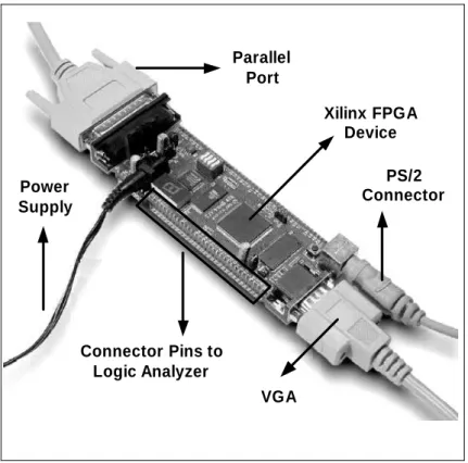
The Integrity Unit architecture (Figure 1) has been captured by using VHDL. All the internal components of the proposed architecture were synthesized placed and routed using a XILINX FPGA device [12]. The system then was simulated again, for the verification of the correct functionality. In order to verify the right operation of the developed system, the test board of Xilinx (XSA Board) was used. This board is shown in the following Figure 6.
Parallel Port Power Supply Connector Pins to Logic Analyzer Xilinx FPGA Device PS/2 Connector VGA
Figure 6: Used FPGA Board
Initially, the developed system is downloaded to the FPGA device by using the parallel computer port. Then, the required VHDL code that permits emulation of the developed architecture is created, and it is downloaded to the board also. The values of the input/output signals were monitored through the help of a logic analyzer, which is connected to the board. (The PS/2 connector and the CRT port are not used in our case). The test scenarios that are applied to the board, in order to verify systems’ correct functionality, are provided by the HMAC, SHA-1 and MD5 standards [4, 9-10]. In addition, during the test procedure a great number of test vectors were used to verify the right operation of the received FPGA device samples. These test vectors, were mostly selected in a random way. Some special values of the input data (for example “FFF…FFF”, “000…000”) have been included also, to ensure maximum test coverage. The right outputs of this extra test vectors can also be verified by the produced outputs of a developed code in a software package such as C++ [10].
The proposed Integrity Unit architecture passed all the above test vectors correctly. In addition, the synthesis results of the introduced Integrity Unit implementation are given in the next section 5.
Springer-Verlag, Vol. 23, No 1, pp. 77-100, 2005.
5. VLSI IMPLEMENTATION RESULTS
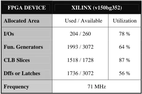
The synthesis results for the proposed Integrity Unit implementation are illustrated in the following Table 3. For the implementation, the XILINX (v150bg352) FPGA device was used. The achieved operating frequency is equal to 71 MHz and the system allocated resources are: 204 I/Os, 1993 Functions Generators and 1518 Configurable Logic Blocks (CLBs). In addition, 1736 Flip-Flops (Dffs) are used.
FPGA DEVICE XILINX (v150bg352)
Allocated Area Used / Available Utilization
I/Os 204 / 260 78 %
Fun. Generators 1993 / 3072 64 %
CLB Slices 1518 / 1728 87 %
Dffs or Latches 1736 / 3072 56 %
Frequency 71 MHz
Table 3: Integrity Unit Synthesis Results
In Table 4, the achievable Hash Function Core (Figure 3) performance, and the covered area resources of the implementation are given. As it has been mentioned in the previous sections, this core is the critical component of the proposed Integrity Unit architecture.
FPGA DEVICE XILINX v150bg352
Allocated Area Used / Available Utilization
I/Os 140 / 260 53 %
Fun. Generators 1303 / 3072 42 %
CLB Slices 1018 / 1728 59 %
Dffs or Latches 1036 / 3072 33 %
Frequency 71 MHz
Table 4: Hash Function Core Implementations Results
A 512-bit data block in MD5 mode, requires 17 clock cycles, in order to be completely processed in the proposed Hash Function Core. In the case of SHA-1 mode, the total process demands 21 clock cycles for a 512-bit data block. In order to have a fair and detail comparison of the proposed unit, comparisons of the proposed Hash Function Core with other published implementations of the same hash functions (SHA-1 and MD5) are presented in Table 5.
Springer-Verlag, Vol. 23, No 1, pp. 77-100, 2005. Hardware / Software Implementations Allocated Area (CLBs) F (MHz) Throughput (Mbps) SHA-1 [13] Software - 133 4.23 41.51 SHA-1 [15] Software 90 40 SHA-1 [14] 1004 43 119 MD5 [15] Software 90 114 MD5 [16] - 300 256 MD5 [14] 1004 43 146 MD5 [17] 880 4763 21 71.4 165 354
Hash Function Core
(SHA-1, MD5) 1718 71
1,7 Gbps SHA-1 2,1 Gbps MD5
Table 5: Hash Functions Implementations Comparison
As the Table 5 illustrates, the proposed Hash Function Core performs better, for both operation modes, compared with the software developments of SHA-1 [13,15] and MD5 [15]. The work [13] is an assembly development in two different kinds of processors. The second processor of [13] operates at 133 MHz while for the first no information is given for the system clock. In the assembly implementation of [15] a 90 MHz processor is used. The performance of these software developments (40-42 Mbps for SHA-1, 114 Mbps for MD5) are too low compared with the achieved performance of the proposed Hash Function Core (1,7 Gbps for SHA-1 and 2,1 Gbps for MD5).
The proposed implementation is better at about 14 times in the term of throughput compared with the FPGA implementation of [14], for SHA-1 operation mode. The proposed Hash Function Core allocates area resources at about 1.7 times more, compared with the same work [14]. The introduced architecture in [14] is designed like a typical processor with data and address buses. This work [14] requires 392 clock cycles to perform the 64 data rounds of MD5 and the 80 rounds of SHA-1. Our proposed unit requires for the cases of SHA-1 and MD5 operation modes, 21 and 17 clock cycles respectively. The shared used arithmetic units in [14], supported by data and address buses, has been proved a design technique with very poor performance, compared with the applied pipeline architecture, based on the full rolling loop technique of the proposed unit. The system throughput of [14], has been sacrificed by the claimed architectural simplicity. From the synthesis results comparisons, it is proven that not good balance between these two different design scopes (simplicity, performance) has not been achieved in [14].
The proposed Hash Function Core, in the case of MD5 operation mode, has better throughput compared with the conventional implementations in all of the cases [14-17]. Especially, compared with the hardware designs of [14, 16, 17] it achieves better throughput at about 14, 8 and 6-13 times respectively. The work [16] provides only a performance estimation of a theoretical MD5 implementation and does not report results of a real hardware implementation. Of course the reported estimations of [16] are still under the readers’ interest. In addition, the first implementation of [17] allocates less covered area than the proposed. This is a physical result of the design [17] rather than a disadvantage of the proposed Hash Function Core. In this work [17], the specified MD5 Padding Unit has not been implemented. The proposed implementation supports this fundamental unit of MD5
Springer-Verlag, Vol. 23, No 1, pp. 77-100, 2005.
specifications. The integration of this unit has consult to a low increment of the allocated area resources. In applications with high speed demands, the 600% better throughput of the proposed architecture is proved superior compared with the first conventional implementation of [17], in spite of the doubled increased area. The second implementation of [17] uses a full-step architecture. Although this design approach achieves doubled performance compared with the first architecture of the same work [17], the covered area resources are increased dramatically by a factor equal to 6. The proposed implementation is superior to the second implementation of [17] both in the covered area resources and the performance.
The full rolling loop technique, applied in our proposed work, is proved a design methodology with better performance, for the implementation of an integrity unit with both MD5 and SHA-1 operation modes. In addition, the pipeline applied technique of our proposed architecture guarantees the very high speed performance. Finally, due to the reconfigurable Data Transformation Rounds design, the allocated area resources are minimized to the lower possible level.
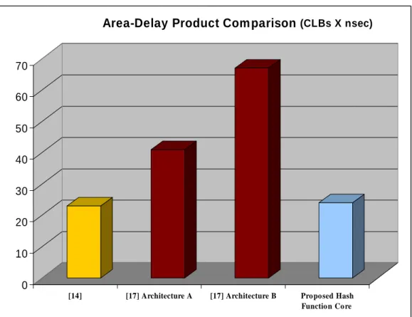
Especially, and only for the hardware implementations the Area-Delay product can be used as a comparison term. This product is calculated easily according to the equation:
Area-Delay Product = Allocated Area (Number of CLBs) X Tdelay (XV)
where Tdelay = 1 / Frequency.
The following Figure 7 shows the Area-Delay Product Comparison.
0 10 20 30 40 50 60 70
[14] [17] Architecture A [17] Architecture B Proposed Hash Function Core Area-Delay Product Com parison (CLBs X nsec)
Figure 7: Area-Delay Product Comparison
From the above figure it is obvious that the proposed architecture has better (less) Area-Delay product compared with both architectures of [17]. The introduced design of [14] has almost the same Area-Delay with the proposed Integrity Unit. Although the great disadvantage of this work [14] is the low throughput, 146 and 119 Mbps, for both MD5 and SHA-1 operation modes respectively,
Springer-Verlag, Vol. 23, No 1, pp. 77-100, 2005.
compared with the proposed Integrity Unit achieved throughput, 2,1 Gbps for MD5 and 1,7 Gbps for SHA-1.
6. CONCLUSIONS AND OBSERVATIONS
In this paper, a VLSI architecture of the Integrity Unit for the OMA security layer is presented. The proposed architecture is reconfigurable in the sense that operates in three different operation modes: HMAC, SHA-1 and MD5. The proposed unit guarantees high security level, in all the applications requiring data integrity and message authentication, via the construction of a message authentication code (HMAC), based on a hash function (SHA-1, and MD5). The proposed architecture has very high-speed performance: 1,7 Gbps for SHA-1 and 2,1 Gbps for MD5. The achieved performance of the SHA-1 operation mode is better at about 14-42 times compared with the other conventional architectures. In addition, the MD5 operation performance is superior to the other related works at about 6-18 times, in all of the cases. These performance results have been achieved by the applied pipeline technique of the proposed architecture. The comparisons of the synthesis results, proved that the proposed Integrity Unit is better, compared with designs with shared used arithmetic units and full step architectures, for the implementation of a powerful Integrity Unit. The achieved performance does not sacrifice the proposed architecture allocated area resources, which have been kept to a minimized level. Furthermore, the proposed Hash Function Core can be used as an independent reconfigurable unit for the operation of both SHA-1 and MD5, instead of the total Integrity Unit (HMAC, SHA-1 and MD5 operations). In this case, the allocated area resources are reduced at about 30%, with no performance penalty.
The above advantages prove that the proposed Integrity Unit is a very trustful and powerful solution for the OMA security layer. In addition, this Integrity Unit can also be integrated in security systems which are used for the implementation of computer networks and wireless protocols in general, with special needs of integrity in data transmission. The introduced Integrity Unit can be used in all the types of HMAC, SHA-1 and MD5 applications, with hard high-speed performance demands (LANs, Wireless Protocols), and with high-level security needs, at the same time.
Springer-Verlag, Vol. 23, No 1, pp. 77-100, 2005.
REFERENCES
[1] “Open Mobile Alliance Specifications”, www.openmobilealliance.org, 2003.
[2] A. Menezes, P.van Oorchot, and S.Vanstone, Handbook of Applied Cryptography, CRC Press, Inc, October 1997.
[3] Bruce Schneier, Applied Cryptography – Protocols, Algorithms and Source Code in C, Second Edition, John Wiley and Sons, New York, 1996.
[4] HMAC Standard, National Institute of Standards and Technology, The Keyed-Hash Message Authentication Code (HMAC), http://csrc.nist.gov/publications/fips/dfips-HMAC.pdf, 2003.
[5] S. Jormalainen and J. Laine, “Security in WTLS”, http://www.hut.fi/~jtlaine2/wtls/, 2003. [6] “SSL Protocol Specifications”, www.netscape.com/eng/ssl3, 2003.
[7] Douglas R. Stinson, “Cryptography: Theory and Practice”, CRC Press LLC, 1995.
[8] S. Bakhtiari, R.Safavi-Naini, J. Pieprzyk, “Cryptographic Hash Functions: A Survey”, Technical Report 95-09, Department of Computer Science, University of Wollongong, July 1995.
[9] R.Rivest, The MD5 Message-Digest Algorithm, RFC 1321, MIT LCS and RSA Data Security, Inc. April 1992.
[10] SHA-1 Standard, National Institute of Standards and Technology (NIST), Secure Hash Standard, FIPS PUB 180-1, www.itl.nist.gov/fipspubs/fip180-1.htm, 2003.
[11] Xilinx, San Jose, California, USA, A simple method of estimating power in XC40000X1/EX/E FPGAs, Application Brief XBRF 014 v1.0, 2003.
[12] Xilinx, San Jose, California, USA, Virtex, 2.5 V Field Programmable Gate Arrays, www.xilinx.com, 2003.
[13] Michael Roe, “Performance of Block Ciphers and Hash Functions-One Year Later”, proceedings of Second International Workshop for Fast Software Encryption ’94, Leuven, Belgium, December 14-16, 1994.
[14] S. Dominikus, “A Hardware Implementation of MD4-Family Hash Algorithms”, proceedings of IEEE International Conference on Electronics Circuits and Systems (ICECS’02), Vol. III, pp.1143-1146, Croatia, September 15-18, 2002.
[15] H. Dobbertin, A. Bosselaers, B. Preneel, “RIPEMD-160, a strengthened version of RIPEMD”, Fast Software Encryption, LNCS 1039, pp. 71-82, Springer-Verlag 1996.
[16] J.D. Touch, “Performance Analysis of MD5”, proceedings of ACM SIGCOMM’95, Cambridge, Massachusetts, 1995.
[17] J. Deepakumara, H.M. Heys, and R. Venkatesan, "FPGA Implementation of MD5 Hash Algorithm", proceedings of IEEE Canadian Conference on Electrical and Computer Engineering (CCECE 2001), Toronto, Ontario, May 2001.
Springer-Verlag, Vol. 23, No 1, pp. 77-100, 2005.
APPENDIX
A. Specifications for SECURE HASH STANDARD (SHA-1)
1.1 Introduction
The Secure Hash Algorithm (SHA-1) is required for use with the Digital Signature Algorithm (DSA) as specified in the Digital Signature Standard (DSS) and whenever a secure hash algorithm is required for federal applications. For a message of length < 2^64 bits, the SHA-1 produces a 160-bit condensed representation of the message called a message digest. The message digest is used during generation of a signature for the message. The SHA-1 is also used to compute a message digest for the received version of the message during the process of verifying the signature. Any change to the message in transit will, with very high probability, result in a different message digest, and the signature will fail to verify. The SHA-1 is designed to have the following properties: it is computationally infeasible to find a message which corresponds to a given message digest, or to find two different messages which produce the same message digest.
1.2 Operations on Words
The following logical operators will be applied to words: X ^ Y = bitwise logical "and" of X and Y.
X \/ Y = bitwise logical "inclusive-or" of X and Y.
X XOR Y = bitwise logical "exclusive-or" of X and Y. ~ X = bitwise logical "complement" of X.
1.3 Message Padding
The SHA-1 is used to compute a message digest for a message or data file that is provided as input. The message or data file should be considered to be a bit string. The length of the message is the number of bits in the message (the empty message has length 0). If the number of bits in a message is a multiple of 8, for compactness we can represent the message in hex. The purpose of message padding is to make the total length of a padded message a multiple of 512. The SHA-1 sequentially processes blocks of 512 bits when computing the message digest. The following specifies how this padding shall be performed. As a summary, a "1" followed by m "0"s followed by a 64-bit integer are appended to the end of the message to produce a padded message of length 512 * n. The 64-bit integer is l, the length of the original message. The padded message is then processed by the SHA-1 as n 512-bit blocks.
1.4 Functions Used
A sequence of logical functions f0, f1,..., f79 is used in the SHA-1. Each ft, 0 <= t <= 79, operates on three 32-bit words B, C, D and produces a 32-bit word as output. ft(B,C,D) is defined as follows, for words B, C, D,
Springer-Verlag, Vol. 23, No 1, pp. 77-100, 2005. ft(B,C,D) = B XOR C XOR D, (20 <= t <= 39) ft(B,C,D) = (B AND C) OR (B AND D) OR (C AND D), (40 <= t <= 59) ft(B,C,D) = B XOR C XOR D, (60 <= t <= 79)
1.5 Constants Used
A sequence of constant words K(0), K(1), ... , K(79) is used in the SHA-1. In hex these are given by Kt = 5A827999 ( 0 <= t <= 19)
Kt = 6ED9EBA1 (20 <= t <= 39) Kt = 8F1BBCDC (40 <= t <= 59) Kt = CA62C1D6 (60 <= t <= 79)
1.6 Computing the Message Digest
The message digest is computed using the final padded message. The computation uses two buffers, each consisting of five 32-bit words, and a sequence of eighty 32-bit words. The words of the first 5-word buffer are labelled A,B,C,D,E. The words of the second 5-word buffer are labelled H0, H1, H2, H3, H4. The words of the 80-word sequence are labelled W0, W1,..., W79. A single word buffer TEMP is also employed. To generate the message digest, the 16-word blocks M1, M2,..., Mn defined in Section 4 are processed in order. The processing of each Mi involves 80 steps. Before processing any blocks, the {Hi} are initialized as follows (in hex):
H0 = 67452301, H1 = EFCDAB89, H2 = 98BADCFE, H3 = 10325476, H4 = C3D2E1F0. Now M1, M2, ... , Mn are processed. To process Mi, we proceed as follows:
a. Divide Mi into 16 words W0, W1, ... , W15, where W0 is the left-most word.
b. For t = 16 to 79 let Wt = S1(Wt-3 XOR Wt-8 XOR Wt- 14 XOR Wt-16).
c. Let A = H0, B = H1, C = H2, D = H3, E = H4. d. For t = 0 to 79 do TEMP = S5(A) + f t(B,C,D) + E + Wt + Kt; E = D; D = C; C = S30(B); B = A; A = TEMP; e. Let H0 = H0 + A, H1 = H1 + B, H2 = H2 + C, H3 = H3 + D, H4 = H4 + E.
After processing Mn, the message digest is the 160-bit string represented by the 5 words H0 H1 H2 H3 and H4.
Springer-Verlag, Vol. 23, No 1, pp. 77-100, 2005.
B. Specifications for MESSAGE DIGEST (MD-5)
2.1 Executive Summary
The algorithm takes as input a message of arbitrary length and produces as output a 128-bit "fingerprint" or "message digest" of the input. It is conjectured that it is computationally infeasible to produce two messages having the same message digest, or to produce any message having a given pre-specified target message digest.
2.2 Terminology and Notation
In this document a "word" is a 32-bit quantity and a "byte" is an eight-bit quantity. A sequence of bits can be interpreted in a natural manner as a sequence of bytes, where each consecutive group of eight bits is interpreted as a byte with the high-order (most significant) bit of each byte listed first. Similarly, a sequence of bytes can be interpreted as a sequence of 32-bit words, where each consecutive group of four bytes is interpreted as a word with the low-order (least significant) byte given first.
Let x_i denote "x sub i". If the subscript is an expression, we surround it in braces, as in x_{i+1}. Similarly, we use ^ for superscripts (exponentiation), so that x^i denotes x to the i-th power. Let the symbol "+" denote addition of words (i.e., modulo-2^32 addition). Let X <<< s denote the 32-bit value obtained by circularly shifting (rotating) X left by s bit positions. Let not(X) denote the bit-wise complement of X, and let X v Y denote the bit-wise OR of X and Y. Let X xor Y denote the bit-wise XOR of X and Y, and let XY denote the bit-wise AND of X and Y.
2.3 MD5 Algorithm Description
We begin by supposing that we have a b-bit message as input, and that we wish to find its message digest. Here b is an arbitrary nonnegative integer; b may be zero, it need not be a multiple of eight, and it may be arbitrarily large. We imagine the bits of the message written down as follows: m_0, m_1,..., m_{b-1}
The following five steps are performed to compute the message digest of the message. Step 1. Append Padding Bits
The message is "padded" (extended) so that its length (in bits) is congruent to 448, modulo 512. That is, the message is extended so that it is just 64 bits shy of being a multiple of 512 bits long. Padding is always performed, even if the length of the message is already congruent to 448, modulo 512. Padding is performed as follows: a single "1" bit is appended to the message, and then "0" bits are appended so that the length in bits of the padded message becomes congruent to 448, modulo 512. In all, at least one bit and at most 512 bits are appended.
Step 2. Append Length
A 64-bit representation of b (the length of the message before the padding bits were added) is appended to the result of the previous step. In the unlikely event that b is greater than 2^64, then only the low-order 64 bits of b are used. These bits are appended as two 32-bit words and appended low-order word first in accordance with the previous conventions. At this point the resulting message (after padding with bits and with b) has a length that is an exact multiple of 512 bits. Equivalently, this
Springer-Verlag, Vol. 23, No 1, pp. 77-100, 2005.
message has a length that is an exact multiple of 16 (32-bit) words. Let M[0 ... N-1] denote the words of the resulting message, where N is a multiple of 16.
Step 3. Initialize MD Buffer
A four-word buffer (A,B,C,D) is used to compute the message digest. Here each of A, B, C, D is a 32-bit register. These registers are initialized to the following values in hexadecimal, low-order bytes first):
word A: 01234567 word B: 89abcdef word C: fedc ba98 word D: 76543210
Step 4. Process Message in 16-Word Blocks
We first define four auxiliary functions that each take as input three 32-bit words and produce as output one 32-bit word.
F(X,Y,Z) = XY v not(X) Z G(X,Y,Z) = XZ v Y not(Z) H(X,Y,Z) = X xor Y xor Z I(X,Y,Z) = Y xor (X v not(Z))
In each bit position F acts as a conditional: if X then Y else Z. The function F could have been defined using + instead of v since XY and not(X)Z will never have 1's in the same bit position.) It is interesting to note that if the bits of X, Y, and Z are independent and unbiased, the each bit of F(X,Y,Z) will be independent and unbiased.The functions G, H, and I are similar to the function F, in that they act in "bitwise parallel" to produce their output from the bits of X, Y, and Z, in such a manner that if the corresponding bits of X, Y, and Z are independent and unbiased, then each bit of G(X,Y,Z), H(X,Y,Z), and I(X,Y,Z) will be independent and unbiased. Note that the function H is the bit-wise "xor" or "parity" function of its inputs. This step uses a 64-element table T[1 ... 64] constructed from the sine function.
Do the following:
/* Process each 16-word block. */ For i = 0 to N/16-1 do
/* Copy block i into X. */ For j = 0 to 15 do
Set X[j] to M[i*16+j]. end /* of loop on j */
/* Save A as AA, B as BB, C as CC, and D as DD. */ AA = A
BB = B CC = C DD = D
Springer-Verlag, Vol. 23, No 1, pp. 77-100, 2005. /* Round 1. */
/* Let [abcd k s i] denote the operation
a = b + ((a + F(b,c,d) + X[k] + T[i]) <<< s). */ /* Do the following 16 operations. */
[ABCD 0 7 1] [DABC 1 12 2] [CDAB 2 17 3] [BCDA 3 22 4] [ABCD 4 7 5] [DABC 5 12 6] [CDAB 6 17 7] [BCDA 7 22 8] [ABCD 8 7 9] [DABC 9 12 10] [CDAB 10 17 11] [BCDA 11 22 12] [ABCD 12 7 13] [DABC 13 12 14] [CDAB 14 17 15] [BCDA 15 22 16] /* Round 2. */
/* Let [abcd k s i] denote the operation
a = b + ((a + G(b,c,d) + X[k] + T[i]) <<< s). */ /* Do the following 16 operations. */
[ABCD 1 5 17] [DABC 6 9 18] [CDAB 11 14 19] [BCDA 0 20 20] [ABCD 5 5 21] [DABC 10 9 22] [CDAB 15 14 23] [BCDA 4 20 24] [ABCD 9 5 25] [DABC 14 9 26] [CDAB 3 14 27] [BCDA 8 20 28] [ABCD 13 5 29] [DABC 2 9 30] [CDAB 7 14 31] [BCDA 12 20 32] /* Round 3. */
/* Let [abcd k s t] denote the operation
a = b + ((a + H(b,c,d) + X[k] + T[i]) <<< s). */ /* Do the following 16 operations. */
[ABCD 5 4 33] [DABC 8 11 34] [CDAB 11 16 35] [BCDA 14 23 36] [ABCD 1 4 37] [DABC 4 11 38] [CDAB 7 16 39] [BCDA 10 23 40] [ABCD 13 4 41] [DABC 0 11 42] [CDAB 3 16 43] [BCDA 6 23 44] [ABCD 9 4 45] [DABC 12 11 46] [CDAB 15 16 47] [BCDA 2 23 48] /* Round 4. */
/* Let [abcd k s t] denote the operation
a = b + ((a + I(b,c,d) + X[k] + T[i]) <<< s). */ /* Do the following 16 operations. */
[ABCD 0 6 49] [DABC 7 10 50] [CDAB 14 15 51] [BCDA 5 21 52] [ABCD 12 6 53] [DABC 3 10 54] [CDAB 10 15 55] [BCDA 1 21 56] [ABCD 8 6 57] [DABC 15 10 58] [CDAB 6 15 59] [BCDA 13 21 60] [ABCD 4 6 61] [DABC 11 10 62] [CDAB 2 15 63] [BCDA 9 21 64]
/* Then perform the following additions. (That is increment each of the four registers by the value it had before this block was started.) */
A = A + AA B = B + BB C = C + CC D = D + DD end /* of loop on i */ Step 5. Output
Springer-Verlag, Vol. 23, No 1, pp. 77-100, 2005.
Nicolas Sklavos, Ph.D. Researcher: He is a PhD Researcher with the Electrical
and Computer Engineering Department, of the University of Patras, Greece. His interests include computer security, new encryption algorithms design, wireless communications, and reconfigurable computing. He holds an award for his PhD thesis on “VLSI Designs of Wireless Communications Security Systems” from IFIP VLSI SOC 2003. He is a referee of International Journals and Conferences. He is a member of the IEEE, the Technical Chamber of Greece, and the Greek Electrical Engineering Society. He has authored or co-authored up to 50 scientific articles in the areas of his research.
Paris Kitsos, Ph.D. Researcher: He is currently pursuing his Ph.D. in the
Department of Electrical and Computer Engineering at the University of Patras, Greece. He received the B.S. in Physics from the University of Patras in 1999. His research interests include VLSI design, hardware implementations of cryptography algorithms, security protocols for wireless communication systems, and Galois field arithmetic implementations. He has published many technical papers in the areas of his research.
Epaminondas Alexopoulos, Student: He is a student of the Department of
Electrical and Computer Engineering at University of Patras, Greece. His research includes hardware implementations, mobile computing and security. He has published papers in the areas of his research.
Odysseas Koufopavlou, Professor: He received the Diploma of Electrical
Engineering in 1983 and the Ph.D. degree in Electrical Engineering in 1990, both from University of Patras, Greece. From 1990 to 1994 he was at the IBM Thomas J. Watson Research Center, Yorktown Heights, NY, USA. He is currently an Associate Professor with the Department of Electrical and Computer Engineering, University of Patras. His research interests include VLSI, low power design, VLSI crypto systems, and high performance communication subsystems architecture and implementation. Dr. Koufopavlou has published more than 100 technical papers and received patents and inventions in these areas.