1. General
description
The LPC1769/68/67/66/65/64/63 are ARM Cortex-M3 based microcontrollers for embedded applications featuring a high level of integration and low power consumption. The ARM Cortex-M3 is a next generation core that offers system enhancements such as enhanced debug features and a higher level of support block integration.
The LPC1768/67/66/65/64/63 operate at CPU frequencies of up to 100 MHz. The LPC1769 operates at CPU frequencies of up to 120 MHz. The ARM Cortex-M3 CPU incorporates a 3-stage pipeline and uses a Harvard architecture with separate local instruction and data buses as well as a third bus for peripherals. The ARM Cortex-M3 CPU also includes an internal prefetch unit that supports speculative branching.
The peripheral complement of the LPC1769/68/67/66/65/64/63 includes up to 512 kB of flash memory, up to 64 kB of data memory, Ethernet MAC, USB Device/Host/OTG interface, 8-channel general purpose DMA controller, 4 UARTs, 2 CAN channels, 2 SSP
controllers, SPI interface, 3 I2C-bus interfaces, 2-input plus 2-output I2S-bus interface,
8-channel 12-bit ADC, 10-bit DAC, motor control PWM, Quadrature Encoder interface, four general purpose timers, 6-output general purpose PWM, ultra-low power Real-Time Clock (RTC) with separate battery supply, and up to 70 general purpose I/O pins.
The LPC1769/68/67/66/65/64/63 are pin-compatible to the 100-pin LPC236x ARM7-based microcontroller series.
For additional documentation, see Section 19 “References”.
2. Features and benefits
ARM Cortex-M3 processor, running at frequencies of up to 100 MHz
(LPC1768/67/66/65/64/63) or of up to 120 MHz (LPC1769). A Memory Protection Unit (MPU) supporting eight regions is included.
ARM Cortex-M3 built-in Nested Vectored Interrupt Controller (NVIC).
Up to 512 kB on-chip flash programming memory. Enhanced flash memory accelerator
enables high-speed 120 MHz operation with zero wait states.
In-System Programming (ISP) and In-Application Programming (IAP) via on-chip
bootloader software.
On-chip SRAM includes:
32/16 kB of SRAM on the CPU with local code/data bus for high-performance CPU
access.
LPC1769/68/67/66/65/64/63
32-bit ARM Cortex-M3 microcontroller; up to 512 kB flash and
64 kB SRAM with Ethernet, USB 2.0 Host/Device/OTG, CAN
Two/one 16 kB SRAM blocks with separate access paths for higher throughput. These SRAM blocks may be used for Ethernet, USB, and DMA memory, as well as for general purpose CPU instruction and data storage.
Eight channel General Purpose DMA controller (GPDMA) on the AHB multilayer
matrix that can be used with SSP, I2S-bus, UART, Analog-to-Digital and
Digital-to-Analog converter peripherals, timer match signals, and for memory-to-memory transfers.
Multilayer AHB matrix interconnect provides a separate bus for each AHB master.
AHB masters include the CPU, General Purpose DMA controller, Ethernet MAC, and the USB interface. This interconnect provides communication with no arbitration delays.
Split APB bus allows high throughput with few stalls between the CPU and DMA.
Serial interfaces:
Ethernet MAC with RMII interface and dedicated DMA controller. (Not available on
all parts, see Table 2.)
USB 2.0 full-speed device/Host/OTG controller with dedicated DMA controller and
on-chip PHY for device, Host, and OTG functions. (Not available on all parts, see
Table 2.)
Four UARTs with fractional baud rate generation, internal FIFO, and DMA support.
One UART has modem control I/O and RS-485/EIA-485 support, and one UART has IrDA support.
CAN 2.0B controller with two channels. (Not available on all parts, see Table 2.)
SPI controller with synchronous, serial, full duplex communication and
programmable data length.
Two SSP controllers with FIFO and multi-protocol capabilities. The SSP interfaces
can be used with the GPDMA controller.
Three enhanced I2C bus interfaces, one with an open-drain output supporting full
I2C specification and Fast mode plus with data rates of 1 Mbit/s, two with standard
port pins. Enhancements include multiple address recognition and monitor mode.
I2S (Inter-IC Sound) interface for digital audio input or output, with fractional rate
control. The I2S-bus interface can be used with the GPDMA. The I2S-bus interface
supports 3-wire and 4-wire data transmit and receive as well as master clock
input/output. (Not available on all parts, see Table 2.)
Other peripherals:
70 (100 pin package) General Purpose I/O (GPIO) pins with configurable
pull-up/down resistors. All GPIOs support a new, configurable open-drain operating mode. The GPIO block is accessed through the AHB multilayer bus for fast access and located in memory such that it supports Cortex-M3 bit banding and use by the General Purpose DMA Controller.
12-bit Analog-to-Digital Converter (ADC) with input multiplexing among eight pins,
conversion rates up to 200 kHz, and multiple result registers. The 12-bit ADC can be used with the GPDMA controller.
10-bit Digital-to-Analog Converter (DAC) with dedicated conversion timer and DMA
support. (Not available on all parts, see Table 2)
Four general purpose timers/counters, with a total of eight capture inputs and ten
compare outputs. Each timer block has an external count input. Specific timer events can be selected to generate DMA requests.
LPC1769_68_67_66_65_64_63 All information provided in this document is subject to legal disclaimers. © NXP Semiconductors N.V. 2015. All rights reserved.
Product data sheet Rev. 9.6 — 18 August 2015 3 of 90
NXP Semiconductors
LPC1769/68/67/66/65/64/63
32-bit ARM Cortex-M3 microcontroller
Quadrature encoder interface that can monitor one external quadrature encoder.
One standard PWM/timer block with external count input.
RTC with a separate power domain and dedicated RTC oscillator. The RTC block
includes 20 bytes of battery-powered backup registers.
WatchDog Timer (WDT). The WDT can be clocked from the internal RC oscillator,
the RTC oscillator, or the APB clock.
ARM Cortex-M3 system tick timer, including an external clock input option.
Repetitive interrupt timer provides programmable and repeating timed interrupts.
Each peripheral has its own clock divider for further power savings.
Standard JTAG debug interface for compatibility with existing tools. Serial Wire Debug
and Serial Wire Trace Port options. Boundary Scan Description Language (BSDL) is not available for this device.
Emulation trace module enables non-intrusive, high-speed real-time tracing of
instruction execution.
Integrated PMU (Power Management Unit) automatically adjusts internal regulators to
minimize power consumption during Sleep, Deep sleep, Power-down, and Deep power-down modes.
Four reduced power modes: Sleep, Deep-sleep, Power-down, and Deep power-down.
Single 3.3 V power supply (2.4 V to 3.6 V).
Four external interrupt inputs configurable as edge/level sensitive. All pins on Port 0
and Port 2 can be used as edge sensitive interrupt sources.
Non-maskable Interrupt (NMI) input.
Clock output function that can reflect the main oscillator clock, IRC clock, RTC clock,
CPU clock, and the USB clock.
The Wake-up Interrupt Controller (WIC) allows the CPU to automatically wake up from
any priority interrupt that can occur while the clocks are stopped in deep sleep, Power-down, and Deep power-down modes.
Processor wake-up from Power-down mode via any interrupt able to operate during
Power-down mode (includes external interrupts, RTC interrupt, USB activity, Ethernet wake-up interrupt, CAN bus activity, Port 0/2 pin interrupt, and NMI).
Brownout detect with separate threshold for interrupt and forced reset.
Power-On Reset (POR).
Crystal oscillator with an operating range of 1 MHz to 25 MHz.
4 MHz internal RC oscillator trimmed to 1 % accuracy that can optionally be used as a
system clock.
PLL allows CPU operation up to the maximum CPU rate without the need for a
high-frequency crystal. May be run from the main oscillator, the internal RC oscillator, or the RTC oscillator.
USB PLL for added flexibility.
Code Read Protection (CRP) with different security levels.
Unique device serial number for identification purposes.
Available as LQFP100 (14 mm 14 mm 1.4 mm), TFBGA1001 (9 mm 9 mm 0.7
mm), and WLCSP100 (5.074 5.074 0.6 mm) package.
3. Applications
4. Ordering
information
4.1 Ordering options
eMetering Alarm systems
Lighting White goods
Industrial networking Motor control
Table 1. Ordering information
Type number Package
Name Description Version
LPC1769FBD100 LQFP100 plastic low profile quad flat package; 100 leads; body 14 14 1.4 mm SOT407-1 LPC1768FBD100 LQFP100 plastic low profile quad flat package; 100 leads; body 14 14 1.4 mm SOT407-1 LPC1768FET100 TFBGA100 plastic thin fine-pitch ball grid array package; 100 balls; body 9 9 0.7 mm SOT926-1 LPC1768UK WLCSP100 wafer level chip-scale package; 100 balls; 5.074 5.074 0.6 mm
-LPC1767FBD100 LQFP100 plastic low profile quad flat package; 100 leads; body 14 14 1.4 mm SOT407-1 LPC1766FBD100 LQFP100 plastic low profile quad flat package; 100 leads; body 14 14 1.4 mm SOT407-1 LPC1765FBD100 LQFP100 plastic low profile quad flat package; 100 leads; body 14 14 1.4 mm SOT407-1 LPC1765FET100 TFBGA100 plastic thin fine-pitch ball grid array package; 100 balls; body 9 9 0.7 mm SOT926-1 LPC1764FBD100 LQFP100 plastic low profile quad flat package; 100 leads; body 14 14 1.4 mm SOT407-1 LPC1763FBD100 LQFP100 plastic low profile quad flat package; 100 leads; body 14 14 1.4 mm SOT407-1
Table 2. Ordering options
Ty p e n u m b e r D evice o rde r p a rt number F lash (kB ) SRAM in kB Ethernet US B CA N I 2S DA C GPIO Max im u m CPU op era tin g f re q ue nc y (MHz) CP U A HB SR AM0 A HB SR AM1 To ta l
LPC1769FBD100 LPC1769FBD100,551 512 32 16 16 64 yes Device/Host/OTG 2 yes yes 70 120 LPC1768FBD100 LPC1768FBD100/CP32 512 32 16 16 64 yes Device/Host/OTG 2 yes yes 70 100 LPC1768FET100 LPC1768FET100Z 512 32 16 16 64 yes Device/Host/OTG 2 yes yes 70 100 LPC1768UK LPC1768UKZ 512 32 16 16 64 yes Device/Host/OTG 2 yes yes 70 100 LPC1767FBD100 LPC1767FBD100,551 512 32 16 16 64 yes no no yes yes 70 100 LPC1766FBD100 LPC1766FBD100,551 256 32 16 16 64 yes Device/Host/OTG 2 yes yes 70 100 LPC1765FBD100 LPC1765FBD100/3271 256 32 16 16 64 no Device/Host/OTG 2 yes yes 70 100 LPC1765FET100 LPC1765FET100,551 256 32 16 16 64 no Device/Host/OTG 2 yes yes 70 100 LPC1764FBD100 LPC1764FBD100,551 128 16 16 - 32 yes Device only 2 no no 70 100 LPC1763FBD100 LPC1763FBD100K 256 32 16 16 64 no no no yes yes 70 100
LPC1769_68_67_66_65_64_63 All information provided in this document is subject to legal disclaimers. © NXP Semiconductors N.V. 2015. All rights reserved.
Product data sheet Rev. 9.6 — 18 August 2015 5 of 90
NXP Semiconductors
LPC1769/68/67/66/65/64/63
32-bit ARM Cortex-M3 microcontroller
5. Marking
The LPC176x devices typically have the following top-side marking: LPC176xxxx
xxxxxxx xxYYWWR[x]
The last/second to last letter in the third line (field ‘R’) will identify the device revision. This data sheet covers the following revisions of the LPC176x:
Field ‘YY’ states the year the device was manufactured. Field ‘WW’ states the week the device was manufactured during that year.
Table 3. Device revision table
Revision identifier (R) Revision description
‘-’ Initial device revision
‘A’ Second device revision
6. Block
diagram
(1) Not available on all parts. See Table 2.
Fig 1. Block diagram
SRAM 32/64 kB ARM CORTEX-M3 TEST/DEBUG INTERFACE EMULA TION TRA CE MODULE FLASH ACCELERATOR FLASH 512/256/128 kB DMA CONTROLLER ETHERNET CONTROLLER WITH DMA(1) USB HOST/ DEVICE/OTG CONTROLLER WITH DMA(1) I-code bus D-code bus system bus AHB TO APB BRIDGE 0 HIGH-SPEED GPIO AHB TO APB BRIDGE 1 CLOCK GENERATION, POWER CONTROL, SYSTEM FUNCTIONS XTAL1 XTAL2 RESET clocks and controls JTAG interface debug port USB PHY SSP0 UART2/3 I2S(1) I2C2 RI TIMER TIMER2/3 EXTERNAL INTERRUPTS SYSTEM CONTROL MOTOR CONTROL PWM QUADRATURE ENCODER SSP1 UART0/1 CAN1/2(1) I2C0/1 SPI0 TIMER 0/1 WDT PWM1 12-bit ADC PIN CONNECT GPIO INTERRUPT CONTROL
RTC
BACKUP REGISTERS 32 kHz
OSCILLATOR
APB slave group 1 APB slave group 0
DAC(1)
RTC POWER DOMAIN
LPC1769/68/67/ 66/65/64/63
master master master
002aad944 slave
slave slave slave
slave
ROM
slave
MULTILAYER AHB MATRIX
P0 to P4 SDA2 SCL2 SCK0 SSEL0 MISO0 MOSI0 SCK1 SSEL1 MISO1 MOSI1 RXD2/3 TXD2/3 PHA, PHB INDEX EINT[3:0] AOUT MCOA[2:0] MCOB[2:0] MCI[2:0] MCABORT 4 × MAT2 2 × MAT3 2 × CAP2 2 × CAP3 3 × I2SRX 3 × I2STX TX_MCLK RX_MCLK RTCX1 RTCX2 VBAT PWM1[7:0] 2 × MAT0/1 2 × CAP0/1 RD1/2 TD1/2 SDA0/1 SCL0/1 AD0[7:0] SCK/SSEL MOSI/MISO 8 × UART1 RXD0/TXD0 P0, P2 PCAP1[1:0]
RMII pins USB pins
CLKOUT
MPU
LPC1769_68_67_66_65_64_63 All information provided in this document is subject to legal disclaimers. © NXP Semiconductors N.V. 2015. All rights reserved.
Product data sheet Rev. 9.6 — 18 August 2015 7 of 90
NXP Semiconductors
LPC1769/68/67/66/65/64/63
32-bit ARM Cortex-M3 microcontroller
7. Pinning
information
7.1 Pinning
Fig 2. Pin configuration LQFP100 package
Fig 3. Pin configuration TFBGA100 package
LPC176xFBD100 50 1 25 75 51 26 76 100 002aad945 002aaf723 LPC1768/65FET100
Transparent top view J G K H F E D C B A 2 4 6 8 10 1 3 5 7 9 ball A1 index area
Fig 4. Pin configuration WLCSP100 package
Transparent top view 1 A B C D E F G H J K 2 3 4 5 6 7 8 9 10 LPC1768UK bump A1 index area aaa-009522
Table 4. Pin allocation table TFBGA100
Pin Symbol Pin Symbol Pin Symbol Pin Symbol
Row A
1 TDO/SWO 2 P0[3]/RXD0/AD0[6] 3 VDD(3V3) 4 P1[4]/ENET_TX_EN
5 P1[10]/ENET_RXD1 6 P1[16]/ENET_MDC 7 VDD(REG)(3V3) 8 P0[4]/I2SRX_CLK/
RD2/CAP2[0] 9 P0[7]/I2STX_CLK/ SCK1/MAT2[1] 10 P0[9]/I2STX_SDA/ MOSI1/MAT2[3] 11 - 12 -Row B 1 TMS/SWDIO 2 RTCK 3 VSS 4 P1[1]/ENET_TXD1 5 P1[9]/ENET_RXD0 6 P1[17]/ ENET_MDIO 7 VSS 8 P0[6]/I2SRX_SDA/ SSEL1/MAT2[0] 9 P2[0]/PWM1[1]/TXD1 10 P2[1]/PWM1[2]/RXD1 11 - 12 -Row C 1 TCK/SWDCLK 2 TRST 3 TDI 4 P0[2]/TXD0/AD0[7] 5 P1[8]/ENET_CRS 6 P1[15]/ ENET_REF_CLK 7 P4[28]/RX_MCLK/ MAT2[0]/TXD3 8 P0[8]/I2STX_WS/ MISO1/MAT2[2] 9 VSS 10 VDD(3V3) 11 - 12 -Row D 1 P0[24]/AD0[1]/ I2SRX_WS/CAP3[1] 2 P0[25]/AD0[2]/ I2SRX_SDA/TXD3 3 P0[26]/AD0[3]/ AOUT/RXD3 4 n.c. 5 P1[0]/ENET_TXD0 6 P1[14]/ENET_RX_ER 7 P0[5]/I2SRX_WS/
TD2/CAP2[1] 8 P2[2]/PWM1[3]/ CTS1/TRACEDATA[3] 9 P2[4]/PWM1[5]/ DSR1/TRACEDATA[1] 10 P2[5]/PWM1[6]/ DTR1/TRACEDATA[0] 11 - 12 -Row E
1 VSSA 2 VDDA 3 VREFP 4 n.c.
5 P0[23]/AD0[0]/ I2SRX_CLK/CAP3[0] 6 P4[29]/TX_MCLK/ MAT2[1]/RXD3 7 P2[3]/PWM1[4]/ DCD1/TRACEDATA[2] 8 P2[6]/PCAP1[0]/ RI1/TRACECLK
LPC1769_68_67_66_65_64_63 All information provided in this document is subject to legal disclaimers. © NXP Semiconductors N.V. 2015. All rights reserved.
Product data sheet Rev. 9.6 — 18 August 2015 9 of 90
NXP Semiconductors
LPC1769/68/67/66/65/64/63
32-bit ARM Cortex-M3 microcontroller
9 P2[7]/RD2/RTS1 10 P2[8]/TD2/TXD2 11 - 12 -Row F 1 VREFN 2 RTCX1 3 RESET 4 P1[31]/SCK1/ AD0[5] 5 P1[21]/MCABORT/ PWM1[3]/SSEL0 6 P0[18]/DCD1/ MOSI0/MOSI 7 P2[9]/USB_CONNECT/ RXD2 8 P0[16]/RXD1/ SSEL0/SSEL 9 P0[17]/CTS1/ MISO0/MISO 10 P0[15]/TXD1/ SCK0/SCK 11 - 12 -Row G
1 RTCX2 2 VBAT 3 XTAL2 4 P0[30]/USB_D
5 P1[25]/MCOA1/ MAT1[1] 6 P1[29]/MCOB2/ PCAP1[1]/MAT0[1] 7 VSS 8 P0[21]/RI1/RD1 9 P0[20]/DTR1/SCL1 10 P0[19]/DSR1/SDA1 11 - 12 -Row H 1 P1[30]/VBUS/ AD0[4] 2 XTAL1 3 P3[25]/MAT0[0]/ PWM1[2] 4 P1[18]/USB_UP_LED/ PWM1[1]/CAP1[0] 5 P1[24]/MCI2/ PWM1[5]/MOSI0 6 VDD(REG)(3V3) 7 P0[10]/TXD2/ SDA2/MAT3[0] 8 P2[11]/EINT1/ I2STX_CLK 9 VDD(3V3) 10 P0[22]/RTS1/TD1 11 - 12
-Table 4. Pin allocation table TFBGA100 …continued
7.2 Pin description
Row J 1 P0[28]/SCL0/ USB_SCL 2 P0[27]/SDA0/ USB_SDA 3 P0[29]/USB_D+ 4 P1[19]/MCOA0/ USB_PPWR/ CAP1[1] 5 P1[22]/MCOB0/ USB_PWRD/ MAT1[0] 6 VSS 7 P1[28]/MCOA2/ PCAP1[0]/ MAT0[0] 8 P0[1]/TD1/RXD3/SCL1 9 P2[13]/EINT3/ I2STX_SDA 10 P2[10]/EINT0/NMI 11 - 12 -Row K 1 P3[26]/STCLK/ MAT0[1]/PWM1[3] 2 VDD(3V3) 3 VSS 4 P1[20]/MCI0/ PWM1[2]/SCK0 5 P1[23]/MCI1/ PWM1[4]/MISO0 6 P1[26]/MCOB1/ PWM1[6]/CAP0[0] 7 P1[27]/CLKOUT /USB_OVRCR/ CAP0[1] 8 P0[0]/RD1/TXD3/SDA1 9 P0[11]/RXD2/ SCL2/MAT3[1] 10 P2[12]/EINT2/ I2STX_WS 11 - 12-Table 4. Pin allocation table TFBGA100 …continued
Pin Symbol Pin Symbol Pin Symbol Pin Symbol
Table 5. Pin description
Symbol Pin/ball Type Description
LQ
FP1
00
TFBGA100 WL
CSP100
P0[0] to P0[31] I/O Port 0: Port 0 is a 32-bit I/O port with individual direction controls for each bit. The operation of port 0 pins depends upon the pin function selected via the pin connect block. Pins 12, 13, 14, and 31 of this port are not available.
P0[0]/RD1/TXD3/ SDA1
46 K8 H10 [1] I/O P0[0] — General purpose digital input/output pin.
I RD1 — CAN1 receiver input. (LPC1769/68/66/65/64 only). O TXD3 — Transmitter output for UART3.
I/O SDA1 — I2C1 data input/output. (This is not an I2C-bus compliant
open-drain pin). P0[1]/TD1/RXD3/
SCL1
47 J8 H9 [1] I/O P0[1] — General purpose digital input/output pin.
O TD1 — CAN1 transmitter output. (LPC1769/68/66/65/64 only). I RXD3 — Receiver input for UART3.
I/O SCL1 — I2C1 clock input/output. (This is not an I2C-bus compliant
open-drain pin).
P0[2]/TXD0/AD0[7] 98 C4 B1 [2] I/O P0[2] — General purpose digital input/output pin.
O TXD0 — Transmitter output for UART0. I AD0[7] — A/D converter 0, input 7.
P0[3]/RXD0/AD0[6] 99 A2 C3 [2] I/O P0[3] — General purpose digital input/output pin.
I RXD0 — Receiver input for UART0. I AD0[6] — A/D converter 0, input 6.
LPC1769_68_67_66_65_64_63 All information provided in this document is subject to legal disclaimers. © NXP Semiconductors N.V. 2015. All rights reserved.
Product data sheet Rev. 9.6 — 18 August 2015 11 of 90
NXP Semiconductors
LPC1769/68/67/66/65/64/63
32-bit ARM Cortex-M3 microcontroller
P0[4]/ I2SRX_CLK/ RD2/CAP2[0]
81 A8 G2 [1] I/O P0[4] — General purpose digital input/output pin.
I/O I2SRX_CLK — Receive Clock. It is driven by the master and received by the slave. Corresponds to the signal SCK in the I2S-bus
specification. (LPC1769/68/67/66/65/63 only).
I RD2 — CAN2 receiver input. (LPC1769/68/66/65/64 only). I CAP2[0] — Capture input for Timer 2, channel 0.
P0[5]/ I2SRX_WS/ TD2/CAP2[1]
80 D7 H1 [1] I/O P0[5] — General purpose digital input/output pin.
I/O I2SRX_WS — Receive Word Select. It is driven by the master and received by the slave. Corresponds to the signal WS in the I2S-bus
specification. (LPC1769/68/67/66/65/63 only).
O TD2 — CAN2 transmitter output. (LPC1769/68/66/65/64 only). I CAP2[1] — Capture input for Timer 2, channel 1.
P0[6]/ I2SRX_SDA/ SSEL1/MAT2[0]
79 B8 G3 [1] I/O P0[6] — General purpose digital input/output pin.
I/O I2SRX_SDA — Receive data. It is driven by the transmitter and read by the receiver. Corresponds to the signal SD in the I2S-bus
specification. (LPC1769/68/67/66/65/63 only). I/O SSEL1 — Slave Select for SSP1.
O MAT2[0] — Match output for Timer 2, channel 0. P0[7]/
I2STX_CLK/ SCK1/MAT2[1]
78 A9 J1 [1] I/O P0[7] — General purpose digital input/output pin.
I/O I2STX_CLK — Transmit Clock. It is driven by the master and received by the slave. Corresponds to the signal SCK in the I2S-bus
specification. (LPC1769/68/67/66/65/63 only). I/O SCK1 — Serial Clock for SSP1.
O MAT2[1] — Match output for Timer 2, channel 1. P0[8]/
I2STX_WS/ MISO1/MAT2[2]
77 C8 H2 [1] I/O P0[8] — General purpose digital input/output pin.
I/O I2STX_WS — Transmit Word Select. It is driven by the master and received by the slave. Corresponds to the signal WS in the I2S-bus
specification. (LPC1769/68/67/66/65/63 only). I/O MISO1 — Master In Slave Out for SSP1. O MAT2[2] — Match output for Timer 2, channel 2. P0[9]/
I2STX_SDA/ MOSI1/MAT2[3]
76 A10 H3 [1] I/O P0[9] — General purpose digital input/output pin.
I/O I2STX_SDA — Transmit data. It is driven by the transmitter and read by the receiver. Corresponds to the signal SD in the I2S-bus
specification. (LPC1769/68/67/66/65/63 only). I/O MOSI1 — Master Out Slave In for SSP1. O MAT2[3] — Match output for Timer 2, channel 3. P0[10]/TXD2/
SDA2/MAT3[0]
48 H7 H8 [1] I/O P0[10] — General purpose digital input/output pin.
O TXD2 — Transmitter output for UART2.
I/O SDA2 — I2C2 data input/output (this is not an open-drain pin).
O MAT3[0] — Match output for Timer 3, channel 0.
Table 5. Pin description …continued
Symbol Pin/ball Type Description
LQ FP10 0 TF BGA 100 WL CSP100
P0[11]/RXD2/ SCL2/MAT3[1]
49 K9 J10 [1] I/O P0[11] — General purpose digital input/output pin.
I RXD2 — Receiver input for UART2.
I/O SCL2 — I2C2 clock input/output (this is not an open-drain pin).
O MAT3[1] — Match output for Timer 3, channel 1. P0[15]/TXD1/
SCK0/SCK
62 F10 H6 [1] I/O P0[15] — General purpose digital input/output pin.
O TXD1 — Transmitter output for UART1. I/O SCK0 — Serial clock for SSP0. I/O SCK — Serial clock for SPI. P0[16]/RXD1/
SSEL0/SSEL
63 F8 J5 [1] I/O P0[16] — General purpose digital input/output pin.
I RXD1 — Receiver input for UART1. I/O SSEL0 — Slave Select for SSP0. I/O SSEL — Slave Select for SPI. P0[17]/CTS1/
MISO0/MISO
61 F9 K6 [1] I/O P0[17] — General purpose digital input/output pin.
I CTS1 — Clear to Send input for UART1. I/O MISO0 — Master In Slave Out for SSP0. I/O MISO — Master In Slave Out for SPI. P0[18]/DCD1/
MOSI0/MOSI
60 F6 J6 [1] I/O P0[18] — General purpose digital input/output pin.
I DCD1 — Data Carrier Detect input for UART1. I/O MOSI0 — Master Out Slave In for SSP0. I/O MOSI — Master Out Slave In for SPI. P0[19]/DSR1/
SDA1
59 G10 K7 [1] I/O P0[19] — General purpose digital input/output pin.
I DSR1 — Data Set Ready input for UART1.
I/O SDA1 — I2C1 data input/output (this is not an I2C-bus compliant
open-drain pin).
P0[20]/DTR1/SCL1 58 G9 J7 [1] I/O P0[20] — General purpose digital input/output pin.
O DTR1 — Data Terminal Ready output for UART1. Can also be configured to be an RS-485/EIA-485 output enable signal. I/O SCL1 — I2C1 clock input/output (this is not an I2C-bus compliant
open-drain pin).
P0[21]/RI1/RD1 57 G8 H7 [1] I/O P0[21] — General purpose digital input/output pin.
I RI1 — Ring Indicator input for UART1.
I RD1 — CAN1 receiver input. (LPC1769/68/66/65/64 only). P0[22]/RTS1/TD1 56 H10 K8 [1] I/O P0[22] — General purpose digital input/output pin.
O RTS1 — Request to Send output for UART1. Can also be configured to be an RS-485/EIA-485 output enable signal. O TD1 — CAN1 transmitter output. (LPC1769/68/66/65/64 only).
Table 5. Pin description …continued
Symbol Pin/ball Type Description
LQ FP10 0 TF BGA 100 WL CSP100
LPC1769_68_67_66_65_64_63 All information provided in this document is subject to legal disclaimers. © NXP Semiconductors N.V. 2015. All rights reserved.
Product data sheet Rev. 9.6 — 18 August 2015 13 of 90
NXP Semiconductors
LPC1769/68/67/66/65/64/63
32-bit ARM Cortex-M3 microcontroller
P0[23]/AD0[0]/ I2SRX_CLK/ CAP3[0]
9 E5 D5 [2] I/O P0[23] — General purpose digital input/output pin.
I AD0[0] — A/D converter 0, input 0.
I/O I2SRX_CLK — Receive Clock. It is driven by the master and received by the slave. Corresponds to the signal SCK in the I2S-bus
specification. (LPC1769/68/67/66/65/63 only). I CAP3[0] — Capture input for Timer 3, channel 0. P0[24]/AD0[1]/
I2SRX_WS/ CAP3[1]
8 D1 B4 [2] I/O P0[24] — General purpose digital input/output pin.
I AD0[1] — A/D converter 0, input 1.
I/O I2SRX_WS — Receive Word Select. It is driven by the master and received by the slave. Corresponds to the signal WS in the I2S-bus
specification. (LPC1769/68/67/66/65/63 only). I CAP3[1] — Capture input for Timer 3, channel 1. P0[25]/AD0[2]/
I2SRX_SDA/ TXD3
7 D2 A3 [2] I/O P0[25] — General purpose digital input/output pin.
I AD0[2] — A/D converter 0, input 2.
I/O I2SRX_SDA — Receive data. It is driven by the transmitter and read by the receiver. Corresponds to the signal SD in the I2S-bus
specification. (LPC1769/68/67/66/65/63 only). O TXD3 — Transmitter output for UART3. P0[26]/AD0[3]/
AOUT/RXD3
6 D3 C5 [3] I/O P0[26] — General purpose digital input/output pin.
I AD0[3] — A/D converter 0, input 3.
O AOUT — DAC output (LPC1769/68/67/66/65/63 only). I RXD3 — Receiver input for UART3.
P0[27]/SDA0/ USB_SDA
25 J2 C8 [4] I/O P0[27] — General purpose digital input/output pin. Output is
open-drain.
I/O SDA0 — I2C0 data input/output. Open-drain output (for I2C-bus
compliance).
I/O USB_SDA — USB port I2C serial data (OTG transceiver,
LPC1769/68/66/65 only). P0[28]/SCL0/
USB_SCL
24 J1 B9 [4] I/O P0[28] — General purpose digital input/output pin. Output is
open-drain.
I/O SCL0 — I2C0 clock input/output. Open-drain output (for I2C-bus
compliance).
I/O USB_SCL — USB port I2C serial clock (OTG transceiver,
LPC1769/68/66/65 only).
P0[29]/USB_D+ 29 J3 B10 [5] I/O P0[29] — General purpose digital input/output pin.
I/O USB_D+ — USB bidirectional D+ line. (LPC1769/68/66/65/64 only). P0[30]/USB_D 30 G4 C9 [5] I/O P0[30] — General purpose digital input/output pin.
I/O USB_D — USB bidirectional D line. (LPC1769/68/66/65/64 only).
Table 5. Pin description …continued
Symbol Pin/ball Type Description
LQ FP10 0 TF BGA 100 WL CSP100
P1[0] to P1[31] I/O Port 1: Port 1 is a 32-bit I/O port with individual direction controls for each bit. The operation of port 1 pins depends upon the pin function selected via the pin connect block. Pins 2, 3, 5, 6, 7, 11, 12, and 13 of this port are not available.
P1[0]/ ENET_TXD0
95 D5 C1 [1] I/O P1[0] — General purpose digital input/output pin.
O ENET_TXD0 — Ethernet transmit data 0. (LPC1769/68/67/66/64 only).
P1[1]/ ENET_TXD1
94 B4 C2 [1] I/O P1[1] — General purpose digital input/output pin.
O ENET_TXD1 — Ethernet transmit data 1. (LPC1769/68/67/66/64 only).
P1[4]/
ENET_TX_EN
93 A4 D2 [1] I/O P1[4] — General purpose digital input/output pin.
O ENET_TX_EN — Ethernet transmit data enable. (LPC1769/68/67/66/64 only).
P1[8]/ ENET_CRS
92 C5 D1 [1] I/O P1[8] — General purpose digital input/output pin.
I ENET_CRS — Ethernet carrier sense. (LPC1769/68/67/66/64 only). P1[9]/
ENET_RXD0
91 B5 D3 [1] I/O P1[9] — General purpose digital input/output pin.
I ENET_RXD0 — Ethernet receive data. (LPC1769/68/67/66/64 only).
P1[10]/ ENET_RXD1
90 A5 E3 [1] I/O P1[10] — General purpose digital input/output pin.
I ENET_RXD1 — Ethernet receive data. (LPC1769/68/67/66/64 only).
P1[14]/ ENET_RX_ER
89 D6 E2 [1] I/O P1[14] — General purpose digital input/output pin.
I ENET_RX_ER — Ethernet receive error. (LPC1769/68/67/66/64 only).
P1[15]/
ENET_REF_CLK
88 C6 E1 [1] I/O P1[15] — General purpose digital input/output pin.
I ENET_REF_CLK — Ethernet reference clock. (LPC1769/68/67/66/64 only).
P1[16]/ ENET_MDC
87 A6 F3 [1] I/O P1[16] — General purpose digital input/output pin.
O ENET_MDC — Ethernet MIIM clock (LPC1769/68/67/66/64 only). P1[17]/
ENET_MDIO
86 B6 F2 [1] I/O P1[17] — General purpose digital input/output pin.
I/O ENET_MDIO — Ethernet MIIM data input and output. (LPC1769/68/67/66/64 only).
Table 5. Pin description …continued
Symbol Pin/ball Type Description
LQ FP10 0 TF BGA 100 WL CSP100
LPC1769_68_67_66_65_64_63 All information provided in this document is subject to legal disclaimers. © NXP Semiconductors N.V. 2015. All rights reserved.
Product data sheet Rev. 9.6 — 18 August 2015 15 of 90
NXP Semiconductors
LPC1769/68/67/66/65/64/63
32-bit ARM Cortex-M3 microcontroller
P1[18]/ USB_UP_LED/ PWM1[1]/ CAP1[0]
32 H4 D9 [1] I/O P1[18] — General purpose digital input/output pin.
O USB_UP_LED — USB GoodLink LED indicator. It is LOW when the device is configured (non-control endpoints enabled), or when the host is enabled and has detected a device on the bus. It is HIGH when the device is not configured, or when host is enabled and has not detected a device on the bus, or during global suspend. It transitions between LOW and HIGH (flashes) when the host is enabled and detects activity on the bus. (LPC1769/68/66/65/64 only).
O PWM1[1] — Pulse Width Modulator 1, channel 1 output. I CAP1[0] — Capture input for Timer 1, channel 0. P1[19]/MCOA0/
USB_PPWR/ CAP1[1]
33 J4 C10 [1] I/O P1[19] — General purpose digital input/output pin.
O MCOA0 — Motor control PWM channel 0, output A. O USB_PPWR — Port Power enable signal for USB port.
(LPC1769/68/66/65 only).
I CAP1[1] — Capture input for Timer 1, channel 1. P1[20]/MCI0/
PWM1[2]/SCK0
34 K4 E8 [1] I/O P1[20] — General purpose digital input/output pin.
I MCI0 — Motor control PWM channel 0, input. Also Quadrature Encoder Interface PHA input.
O PWM1[2] — Pulse Width Modulator 1, channel 2 output. I/O SCK0 — Serial clock for SSP0.
P1[21]/MCABORT/ PWM1[3]/
SSEL0
35 F5 E9 [1] I/O P1[21] — General purpose digital input/output pin.
O MCABORT — Motor control PWM, LOW-active fast abort. O PWM1[3] — Pulse Width Modulator 1, channel 3 output. I/O SSEL0 — Slave Select for SSP0.
P1[22]/MCOB0/ USB_PWRD/ MAT1[0]
36 J5 D10 [1] I/O P1[22] — General purpose digital input/output pin.
O MCOB0 — Motor control PWM channel 0, output B.
I USB_PWRD — Power Status for USB port (host power switch, LPC1769/68/66/65 only).
O MAT1[0] — Match output for Timer 1, channel 0. P1[23]/MCI1/
PWM1[4]/MISO0
37 K5 E7 [1] I/O P1[23] — General purpose digital input/output pin.
I MCI1 — Motor control PWM channel 1, input. Also Quadrature Encoder Interface PHB input.
O PWM1[4] — Pulse Width Modulator 1, channel 4 output. I/O MISO0 — Master In Slave Out for SSP0.
P1[24]/MCI2/ PWM1[5]/MOSI0
38 H5 F8 [1] I/O P1[24] — General purpose digital input/output pin.
I MCI2 — Motor control PWM channel 2, input. Also Quadrature Encoder Interface INDEX input.
O PWM1[5] — Pulse Width Modulator 1, channel 5 output. I/O MOSI0 — Master Out Slave in for SSP0.
Table 5. Pin description …continued
Symbol Pin/ball Type Description
LQ FP10 0 TF BGA 100 WL CSP100
P1[25]/MCOA1/ MAT1[1]
39 G5 F9 [1] I/O P1[25] — General purpose digital input/output pin.
O MCOA1 — Motor control PWM channel 1, output A. O MAT1[1] — Match output for Timer 1, channel 1. P1[26]/MCOB1/
PWM1[6]/CAP0[0]
40 K6 E10 [1] I/O P1[26] — General purpose digital input/output pin.
O MCOB1 — Motor control PWM channel 1, output B. O PWM1[6] — Pulse Width Modulator 1, channel 6 output. I CAP0[0] — Capture input for Timer 0, channel 0. P1[27]/CLKOUT
/USB_OVRCR/ CAP0[1]
43 K7 G9 [1] I/O P1[27] — General purpose digital input/output pin.
O CLKOUT — Clock output pin.
I USB_OVRCR — USB port Over-Current status. (LPC1769/68/66/65 only).
I CAP0[1] — Capture input for Timer 0, channel 1. P1[28]/MCOA2/
PCAP1[0]/ MAT0[0]
44 J7 G10 [1] I/O P1[28] — General purpose digital input/output pin.
O MCOA2 — Motor control PWM channel 2, output A. I PCAP1[0] — Capture input for PWM1, channel 0. O MAT0[0] — Match output for Timer 0, channel 0. P1[29]/MCOB2/
PCAP1[1]/ MAT0[1]
45 G6 G8 [1] I/O P1[29] — General purpose digital input/output pin.
O MCOB2 — Motor control PWM channel 2, output B. I PCAP1[1] — Capture input for PWM1, channel 1. O MAT0[1] — Match output for Timer 0, channel 1. P1[30]/VBUS/
AD0[4]
21 H1 B8 [2] I/O P1[30] — General purpose digital input/output pin.
I VBUS — Monitors the presence of USB bus power.
(LPC1769/68/66/65/64 only).
Note: This signal must be HIGH for USB reset to occur. I AD0[4] — A/D converter 0, input 4.
P1[31]/SCK1/ AD0[5]
20 F4 C7 [2] I/O P1[31] — General purpose digital input/output pin.
I/O SCK1 — Serial Clock for SSP1. I AD0[5] — A/D converter 0, input 5.
P2[0] to P2[31] I/O Port 2: Port 2 is a 32-bit I/O port with individual direction controls for each bit. The operation of port 2 pins depends upon the pin function selected via the pin connect block. Pins 14 through 31 of this port are not available.
P2[0]/PWM1[1]/ TXD1
75 B9 K1 [1] I/O P2[0] — General purpose digital input/output pin.
O PWM1[1] — Pulse Width Modulator 1, channel 1 output. O TXD1 — Transmitter output for UART1.
P2[1]/PWM1[2]/ RXD1
74 B10 J2 [1] I/O P2[1] — General purpose digital input/output pin.
O PWM1[2] — Pulse Width Modulator 1, channel 2 output. I RXD1 — Receiver input for UART1.
Table 5. Pin description …continued
Symbol Pin/ball Type Description
LQ FP10 0 TF BGA 100 WL CSP100
LPC1769_68_67_66_65_64_63 All information provided in this document is subject to legal disclaimers. © NXP Semiconductors N.V. 2015. All rights reserved.
Product data sheet Rev. 9.6 — 18 August 2015 17 of 90
NXP Semiconductors
LPC1769/68/67/66/65/64/63
32-bit ARM Cortex-M3 microcontroller
P2[2]/PWM1[3]/ CTS1/
TRACEDATA[3]
73 D8 K2 [1] I/O P2[2] — General purpose digital input/output pin.
O PWM1[3] — Pulse Width Modulator 1, channel 3 output. I CTS1 — Clear to Send input for UART1.
O TRACEDATA[3] — Trace data, bit 3. P2[3]/PWM1[4]/
DCD1/
TRACEDATA[2]
70 E7 K3 [1] I/O P2[3] — General purpose digital input/output pin.
O PWM1[4] — Pulse Width Modulator 1, channel 4 output. I DCD1 — Data Carrier Detect input for UART1.
O TRACEDATA[2] — Trace data, bit 2. P2[4]/PWM1[5]/
DSR1/
TRACEDATA[1]
69 D9 J3 [1] I/O P2[4] — General purpose digital input/output pin.
O PWM1[5] — Pulse Width Modulator 1, channel 5 output. I DSR1 — Data Set Ready input for UART1.
O TRACEDATA[1] — Trace data, bit 1. P2[5]/PWM1[6]/
DTR1/
TRACEDATA[0]
68 D10 H4 [1] I/O P2[5] — General purpose digital input/output pin.
O PWM1[6] — Pulse Width Modulator 1, channel 6 output. O DTR1 — Data Terminal Ready output for UART1. Can also be
configured to be an RS-485/EIA-485 output enable signal. O TRACEDATA[0] — Trace data, bit 0.
P2[6]/PCAP1[0]/ RI1/TRACECLK
67 E8 K4 [1] I/O P2[6] — General purpose digital input/output pin.
I PCAP1[0] — Capture input for PWM1, channel 0. I RI1 — Ring Indicator input for UART1.
O TRACECLK — Trace Clock. P2[7]/RD2/
RTS1
66 E9 J4 [1] I/O P2[7] — General purpose digital input/output pin.
I RD2 — CAN2 receiver input. (LPC1769/68/66/65/64 only). O RTS1 — Request to Send output for UART1. Can also be
configured to be an RS-485/EIA-485 output enable signal. P2[8]/TD2/
TXD2
65 E10 H5 [1] I/O P2[8] — General purpose digital input/output pin.
O TD2 — CAN2 transmitter output. (LPC1769/68/66/65/64 only). O TXD2 — Transmitter output for UART2.
P2[9]/
USB_CONNECT/ RXD2
64 F7 K5 [1] I/O P2[9] — General purpose digital input/output pin.
O USB_CONNECT — Signal used to switch an external 1.5 k resistor under software control. Used with the SoftConnect USB feature. (LPC1769/68/66/65/64 only).
I RXD2 — Receiver input for UART2.
P2[10]/EINT0/NMI 53 J10 K9 [6] I/O P2[10] — General purpose digital input/output pin. A LOW level on
this pin during reset starts the ISP command handler. I EINT0 — External interrupt 0 input.
I NMI — Non-maskable interrupt input.
Table 5. Pin description …continued
Symbol Pin/ball Type Description
LQ FP10 0 TF BGA 100 WL CSP100
P2[11]/EINT1/ I2STX_CLK
52 H8 J8 [6] I/O P2[11] — General purpose digital input/output pin.
I EINT1 — External interrupt 1 input.
I/O I2STX_CLK — Transmit Clock. It is driven by the master and received by the slave. Corresponds to the signal SCK in the I2S-bus
specification. (LPC1769/68/67/66/65/63 only). P2[12]/EINT2/
I2STX_WS
51 K10 K10 [6] I/O P2[12] — General purpose digital input/output pin.
I EINT2 — External interrupt 2 input.
I/O I2STX_WS — Transmit Word Select. It is driven by the master and received by the slave. Corresponds to the signal WS in the I2S-bus
specification. (LPC1769/68/67/66/65/63 only). P2[13]/EINT3/
I2STX_SDA
50 J9 J9 [6] I/O P2[13] — General purpose digital input/output pin.
I EINT3 — External interrupt 3 input.
I/O I2STX_SDA — Transmit data. It is driven by the transmitter and read by the receiver. Corresponds to the signal SD in the I2S-bus
specification. (LPC1769/68/67/66/65/63 only).
P3[0] to P3[31] I/O Port 3: Port 3 is a 32-bit I/O port with individual direction controls for each bit. The operation of port 3 pins depends upon the pin function selected via the pin connect block. Pins 0 through 24, and 27 through 31 of this port are not available.
P3[25]/MAT0[0]/ PWM1[2]
27 H3 D8 [1] I/O P3[25] — General purpose digital input/output pin.
O MAT0[0] — Match output for Timer 0, channel 0. O PWM1[2] — Pulse Width Modulator 1, output 2. P3[26]/STCLK/
MAT0[1]/PWM1[3]
26 K1 A10 [1] I/O P3[26] — General purpose digital input/output pin.
I STCLK — System tick timer clock input. The maximum STCLK frequency is 1/4 of the ARM processor clock frequency CCLK. O MAT0[1] — Match output for Timer 0, channel 1.
O PWM1[3] — Pulse Width Modulator 1, output 3.
P4[0] to P4[31] I/O Port 4: Port 4 is a 32-bit I/O port with individual direction controls for each bit. The operation of port 4 pins depends upon the pin function selected via the pin connect block. Pins 0 through 27, 30, and 31 of this port are not available.
P4[28]/RX_MCLK/ MAT2[0]/TXD3
82 C7 G1 [1] I/O P4[28] — General purpose digital input/output pin.
O RX_MCLK — I2S receive master clock. (LPC1769/68/67/66/65
only).
O MAT2[0] — Match output for Timer 2, channel 0. O TXD3 — Transmitter output for UART3.
P4[29]/TX_MCLK/ MAT2[1]/RXD3
85 E6 F1 [1] I/O P4[29] — General purpose digital input/output pin.
O TX_MCLK — I2S transmit master clock. (LPC1769/68/67/66/65
only).
O MAT2[1] — Match output for Timer 2, channel 1. I RXD3 — Receiver input for UART3.
Table 5. Pin description …continued
Symbol Pin/ball Type Description
LQ FP10 0 TF BGA 100 WL CSP100
LPC1769_68_67_66_65_64_63 All information provided in this document is subject to legal disclaimers. © NXP Semiconductors N.V. 2015. All rights reserved.
Product data sheet Rev. 9.6 — 18 August 2015 19 of 90
NXP Semiconductors
LPC1769/68/67/66/65/64/63
32-bit ARM Cortex-M3 microcontroller
TDO/SWO 1 A1 A1 [7] O TDO — Test Data out for JTAG interface.
O SWO — Serial wire trace output.
TDI 2 C3 C4 [1][8] I TDI — Test Data in for JTAG interface.
TMS/SWDIO 3 B1 B3 [1][8] I TMS — Test Mode Select for JTAG interface.
I/O SWDIO — Serial wire debug data input/output.
TRST 4 C2 A2 [1][8] I TRST — Test Reset for JTAG interface.
TCK/SWDCLK 5 C1 D4 [7] I TCK — Test Clock for JTAG interface.
I SWDCLK — Serial wire clock.
RTCK 100 B2 B2 [7] O RTCK — JTAG interface control signal.
RSTOUT 14 - - - O RSTOUT — This is a 3.3 V pin. LOW on this pin indicates the microcontroller being in Reset state.
RESET 17 F3 C6 [9] I External reset input: A LOW-going pulse as short as 50 ns on this
pin resets the device, causing I/O ports and peripherals to take on their default states, and processor execution to begin at address 0. TTL with hysteresis, 5 V tolerant.
XTAL1 22 H2 D7 [10][11] I Input to the oscillator circuit and internal clock generator circuits.
XTAL2 23 G3 A9 [10][11] O Output from the oscillator amplifier.
RTCX1 16 F2 A7 [10][11] I Input to the RTC oscillator circuit.
RTCX2 18 G1 B7 [10] O Output from the RTC oscillator circuit.
VSS 31, 41, 55, 72, 83, 97 B3, B7, C9, G7, J6, K3 E5, F5, F6, G5, G6, G7 [10] I ground: 0 V reference.
VSSA 11 E1 B5 [10] I analog ground: 0 V reference. This should nominally be the same
voltage as VSS, but should be isolated to minimize noise and error.
VDD(3V3) 28, 54, 71, 96 K2, H9, C10 , A3 E4, E6, F7, G4
[10] I 3.3 V supply voltage: This is the power supply voltage for the I/O
ports. VDD(REG)(3V3) 42, 84 H6, A7 F4, F10
[10] I 3.3 V voltage regulator supply voltage: This is the supply voltage
for the on-chip voltage regulator only.
VDDA 10 E2 A4 [10] I analog 3.3 V pad supply voltage: This should be nominally the
same voltage as VDD(3V3) but should be isolated to minimize noise
and error. This voltage is used to power the ADC and DAC. This pin should be tied to 3.3 V if the ADC and DAC are not used.
VREFP 12 E3 A5 [10] I ADC positive reference voltage: This should be nominally the
same voltage as VDDA but should be isolated to minimize noise and
error. Level on this pin is used as a reference for ADC and DAC. This pin should be tied to 3.3 V if the ADC and DAC are not used.
Table 5. Pin description …continued
Symbol Pin/ball Type Description
LQ FP10 0 TF BGA 100 WL CSP100
[1] 5 V tolerant pad providing digital I/O functions with TTL levels and hysteresis. This pin is pulled up to a voltage level of 2.3 V to 2.6 V. [2] 5 V tolerant pad providing digital I/O functions (with TTL levels and hysteresis) and analog input. When configured as a ADC input,
digital section of the pad is disabled and the pin is not 5 V tolerant. This pin is pulled up to a voltage level of 2.3 V to 2.6 V.
[3] 5 V tolerant pad providing digital I/O with TTL levels and hysteresis and analog output function. When configured as the DAC output, digital section of the pad is disabled. This pin is pulled up to a voltage level of 2.3 V to 2.6 V.
[4] Open-drain 5 V tolerant digital I/O pad, compatible with I2C-bus 400 kHz specification. This pad requires an external pull-up to provide output functionality. When power is switched off, this pin connected to the I2C-bus is floating and does not disturb the I2C lines. Open-drain configuration applies to all functions on this pin.
[5] Pad provides digital I/O and USB functions. It is designed in accordance with the USB specification, revision 2.0 (Full-speed and Low-speed mode only). This pad is not 5 V tolerant.
[6] 5 V tolerant pad with 10 ns glitch filter providing digital I/O functions with TTL levels and hysteresis. This pin is pulled up to a voltage level of 2.3 V to 2.6 V.
[7] 5 V tolerant pad with TTL levels and hysteresis. Internal pull-up and pull-down resistors disabled. [8] 5 V tolerant pad with TTL levels and hysteresis and internal pull-up resistor.
[9] 5 V tolerant pad with 20 ns glitch filter providing digital I/O function with TTL levels and hysteresis. [10] Pad provides special analog functionality. A 32 kHz crystal oscillator must be used with the RTC.
[11] When the system oscillator is not used, connect XTAL1 and XTAL2 as follows: XTAL1 can be left floating or can be grounded (grounding is preferred to reduce susceptibility to noise). XTAL2 should be left floating.
[12] When the RTC is not used, connect VBAT to VDD(REG)(3V3) and leave RTCX1 floating.
VREFN 15 F1 A6 I ADC negative reference voltage: This should be nominally the same voltage as VSS but should be isolated to minimize noise and
error. Level on this pin is used as a reference for ADC and DAC. VBAT 19 G2 A8 [10][12] I RTC pin power supply: 3.3 V on this pin supplies the power to the
RTC peripheral. n.c. 13 D4, E4 B6, D6 - not connected.
Table 5. Pin description …continued
Symbol Pin/ball Type Description
LQ FP10 0 TF BGA 100 WL CSP100
LPC1769_68_67_66_65_64_63 All information provided in this document is subject to legal disclaimers. © NXP Semiconductors N.V. 2015. All rights reserved.
Product data sheet Rev. 9.6 — 18 August 2015 21 of 90
NXP Semiconductors
LPC1769/68/67/66/65/64/63
32-bit ARM Cortex-M3 microcontroller
8. Functional
description
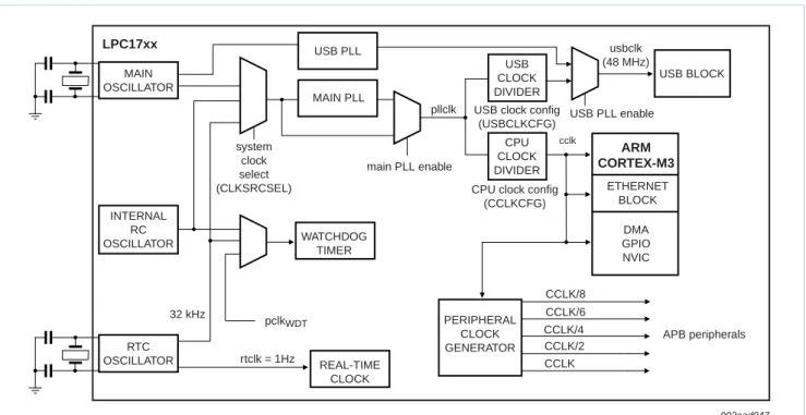
8.1 Architectural overview
Remark: In the following, the notation LPC17xx refers to all parts: LPC1769/68/67/66/65/64/63.
The ARM Cortex-M3 includes three AHB-Lite buses: the system bus, the I-code bus, and
the D-code bus (see Figure 1). The I-code and D-code core buses are faster than the
system bus and are used similarly to TCM interfaces: one bus dedicated for instruction fetch (I-code) and one bus for data access (D-code). The use of two core buses allows for simultaneous operations if concurrent operations target different devices.
The LPC17xx use a multi-layer AHB matrix to connect the ARM Cortex-M3 buses and other bus masters to peripherals in a flexible manner that optimizes performance by allowing peripherals that are on different slaves ports of the matrix to be accessed simultaneously by different bus masters.
8.2 ARM Cortex-M3 processor
The ARM Cortex-M3 is a general purpose, 32-bit microprocessor, which offers high performance and very low power consumption. The ARM Cortex-M3 offers many new features, including a Thumb-2 instruction set, low interrupt latency, hardware divide, interruptible/continuable multiple load and store instructions, automatic state save and restore for interrupts, tightly integrated interrupt controller with wake-up interrupt controller, and multiple core buses capable of simultaneous accesses.
Pipeline techniques are employed so that all parts of the processing and memory systems can operate continuously. Typically, while one instruction is being executed, its successor is being decoded, and a third instruction is being fetched from memory.
The ARM Cortex-M3 processor is described in detail in the Cortex-M3 Technical
Reference Manual that can be found on official ARM website.
8.3 On-chip flash program memory
The LPC17xx contain up to 512 kB of on-chip flash memory. A new two-port flash accelerator maximizes performance for use with the two fast AHB-Lite buses.
8.4 On-chip SRAM
The LPC17xx contain a total of 64 kB on-chip static RAM memory. This includes the main 32 kB SRAM, accessible by the CPU and DMA controller on a higher-speed bus, and two additional 16 kB each SRAM blocks situated on a separate slave port on the AHB multilayer matrix.
This architecture allows CPU and DMA accesses to be spread over three separate RAMs that can be accessed simultaneously.
8.5 Memory Protection Unit (MPU)
The LPC17xx have a Memory Protection Unit (MPU) which can be used to improve the reliability of an embedded system by protecting critical data within the user application.
The MPU allows separating processing tasks by disallowing access to each other's data, disabling access to memory regions, allowing memory regions to be defined as read-only and detecting unexpected memory accesses that could potentially break the system. The MPU separates the memory into distinct regions and implements protection by preventing disallowed accesses. The MPU supports up to 8 regions each of which can be divided into 8 subregions. Accesses to memory locations that are not defined in the MPU regions, or not permitted by the region setting, will cause the Memory Management Fault exception to take place.
8.6 Memory map
The LPC17xx incorporates several distinct memory regions, shown in the following
figures. Figure 5 shows the overall map of the entire address space from the user
program viewpoint following reset. The interrupt vector area supports address remapping. The AHB peripheral area is 2 MB in size and is divided to allow for up to 128 peripherals. The APB peripheral area is 1 MB in size and is divided to allow for up to 64 peripherals. Each peripheral of either type is allocated 16 kB of space. This allows simplifying the address decoding for each peripheral.
xxxxxxxxxxxxxxxxxxxxx xxxxxxxxxxxxxxxxxxxxxxxxxx xxxxxxx x x x xxxxxxxxxxxxxxxxxxxxxxxxxxxxxx xxxxxxxxxxxxxxxxxxx xx xx xxxxx xxxxxxxxxxxxxxxxxxxxxxxxxxx xxxxxxxxxxxxxxxxxxx xxxxxx xxxxxxxxxxxxxxxxxxxxxxxxxxxxxxxxxxx xxxxxxxxxxxx x x xxxxxxxxxxxxxxxxxxxxx xxxxxxxxxxxxxxxxxxxxxxxxxxxxxx xxxxx xxxxxxxxxxxxxxxxxxxxxxxxxxxxxxxxxxxxxxxxxxxxxxxxxx xxxxxxxx xxxxxxxxxxxxxxxxxxxxxxxxx xxxxxxxxxxxxxxxxxxxx xxx LP C1769 _68_6 7_66 _65_ 64_6 3 A ll i nfor m at ion pr ovi ded in this do cum ent i s sub jec t to leg al d is c laim er s. © NXP Se mic on duc tor s N.V . 20 15. Al l r ig h ts r e s e rv ed. Produ ct d at a sheet Rev . 9.6 — 18 Au gu st 2015 23 o f 90
N
X
P Semi
conductor
s
LPC1769/68/67/66/65/64/63
32-bit ARM Cor tex -M 3 mic roco ntr olle r(1) Not available on all parts. See Table 2. Fig 5. LPC17xx memory map
0x5000 0000 0x5000 4000 0x5000 8000 0x5000 C000 0x5020 0000 0x5001 0000 AHB peripherals Ethernet controller(1) USB controller(1) reserved 127- 4 reserved GPDMA controller 0 1 2 3 APB0 peripherals 0x4000 4000 0x4000 8000 0x4000 C000 0x4001 0000 0x4001 8000 0x4002 0000 0x4002 8000 0x4002 C000 0x4003 4000 0x4003 0000 0x4003 8000 0x4003 C000 0x4004 0000 0x4004 4000 0x4004 8000 0x4004 C000 0x4005 C000 0x4006 0000 0x4008 0000 0x4002 4000 0x4001 C000 0x4001 4000 0x4000 0000 WDT timer 0 timer 1 UART0 UART1 reserved I2C0 SPI RTC + backup registers GPIO interrupts pin connect SSP1 ADC CAN AF RAM(1) CAN AF registers(1) CAN common(1) CAN1(1) CAN2(1) 22 - 19 reserved I2C1 31 - 24 reserved 0 1 2 3 4 5 6 7 8 9 10 11 12 13 14 15 16 17 18 23 reserved reserved 32 kB local SRAM (LPC1769/8/7/6/5/3) 16 kB local SRAM (LPC1764) reserved reserved private peripheral bus
0x0000 0000 0 GB 0.5 GB 4 GB 1 GB 0x0004 0000 0x0002 0000 0x0008 0000 0x1000 4000 0x1000 0000 0x1000 8000 0x1FFF 0000 0x1FFF 2000 0x2008 0000 0x2007 C000 0x2008 4000 0x2200 0000 0x200A 0000 0x2009 C000 0x2400 0000 0x4000 0000 0x4008 0000 0x4010 0000 0x4200 0000 0x4400 0000 0x5000 0000 0x5020 0000 0xE000 0000 0xE010 0000 0xFFFF FFFF reserved reserved GPIO reserved reserved reserved reserved APB0 peripherals AHB peripherals APB1 peripherals
AHB SRAM bit-band alias addressing peripheral bit-band alias addressing
16 kB AHB SRAM1 (LPC1769/8/7/6/5) 16 kB AHB SRAM0 256 kB on-chip flash (LPC1766/65/63) 128 kB on-chip flash (LPC1764) 512 kB on-chip flash (LPC1769/8/7) PWM1 8 kB boot ROM 0x0000 0000 0x0000 0400
active interrupt vectors
+ 256 words I-code/D-code memory space 002aad946 APB1 peripherals 0x4008 0000 0x4008 8000 0x4008 C000 0x4009 0000 0x4009 4000 0x4009 8000 0x4009 C000 0x400A 0000 0x400A 4000 0x400A 8000 0x400A C000 0x400B 0000 0x400B 4000 0x400B 8000 0x400B C000 0x400C 0000 0x400F C000 0x4010 0000 SSP0 DAC(1) timer 2 timer 3 UART2 UART3 reserved I2S(1) I2C2 1 - 0 reserved 2 3 4 5 6 7 8 9 10 reserved repetitive interrupt timer 11 12 reserved motor control PWM 30 - 16 reserved 13 14 15 system control 31 QEI LPC1769/68/67/66/65/64/63
8.7 Nested Vectored Interrupt Controller (NVIC)
The NVIC is an integral part of the Cortex-M3. The tight coupling to the CPU allows for low interrupt latency and efficient processing of late arriving interrupts.
8.7.1 Features
•
Controls system exceptions and peripheral interrupts•
In the LPC17xx, the NVIC supports 33 vectored interrupts•
32 programmable interrupt priority levels, with hardware priority level masking•
Relocatable vector table•
Non-Maskable Interrupt (NMI)•
Software interrupt generation8.7.2 Interrupt sources
Each peripheral device has one interrupt line connected to the NVIC but may have several interrupt flags. Individual interrupt flags may also represent more than one interrupt source.
Any pin on Port 0 and Port 2 (total of 42 pins) regardless of the selected function, can be programmed to generate an interrupt on a rising edge, a falling edge, or both.
8.8 Pin connect block
The pin connect block allows selected pins of the microcontroller to have more than one function. Configuration registers control the multiplexers to allow connection between the pin and the on-chip peripherals.
Peripherals should be connected to the appropriate pins prior to being activated and prior to any related interrupt(s) being enabled. Activity of any enabled peripheral function that is not mapped to a related pin should be considered undefined.
Most pins can also be configured as open-drain outputs or to have a pull-up, pull-down, or no resistor enabled.
8.9 General purpose DMA controller
The GPDMA is an AMBA AHB compliant peripheral allowing selected peripherals to have DMA support.
The GPDMA enables peripheral-to-memory, memory-to-peripheral,
peripheral-to-peripheral, and memory-to-memory transactions. The source and destination areas can each be either a memory region or a peripheral, and can be accessed through the AHB master. The GPDMA controller allows data transfers between the USB and Ethernet controllers and the various on-chip SRAM areas. The supported
APB peripherals are SSP0/1, all UARTs, the I2S-bus interface, the ADC, and the DAC.
Two match signals for each timer can be used to trigger DMA transfers.
Remark: The Ethernet controller is available on parts LPC1769/68/67/66/64. The USB
controller is available on parts LPC1769/68/66/65/64. The I2S-bus interface is available on
LPC1769_68_67_66_65_64_63 All information provided in this document is subject to legal disclaimers. © NXP Semiconductors N.V. 2015. All rights reserved.
Product data sheet Rev. 9.6 — 18 August 2015 25 of 90
NXP Semiconductors
LPC1769/68/67/66/65/64/63
32-bit ARM Cortex-M3 microcontroller
8.9.1 Features
•
Eight DMA channels. Each channel can support an unidirectional transfer.•
16 DMA request lines.•
Single DMA and burst DMA request signals. Each peripheral connected to the DMAController can assert either a burst DMA request or a single DMA request. The DMA burst size is set by programming the DMA Controller.
•
Memory-to-memory, memory-to-peripheral, peripheral-to-memory, andperipheral-to-peripheral transfers are supported.
•
Scatter or gather DMA is supported through the use of linked lists. This means thatthe source and destination areas do not have to occupy contiguous areas of memory.
•
Hardware DMA channel priority.•
AHB slave DMA programming interface. The DMA Controller is programmed bywriting to the DMA control registers over the AHB slave interface.
•
One AHB bus master for transferring data. The interface transfers data when a DMArequest goes active.
•
32-bit AHB master bus width.•
Incrementing or non-incrementing addressing for source and destination.•
Programmable DMA burst size. The DMA burst size can be programmed to moreefficiently transfer data.
•
Internal four-word FIFO per channel.•
Supports 8, 16, and 32-bit wide transactions.•
Big-endian and little-endian support. The DMA Controller defaults to little-endianmode on reset.
•
An interrupt to the processor can be generated on a DMA completion or when a DMAerror has occurred.
•
Raw interrupt status. The DMA error and DMA count raw interrupt status can be readprior to masking.
8.10 Fast general purpose parallel I/O
Device pins that are not connected to a specific peripheral function are controlled by the GPIO registers. Pins may be dynamically configured as inputs or outputs. Separate registers allow setting or clearing any number of outputs simultaneously. The value of the output register may be read back as well as the current state of the port pins.
LPC17xx use accelerated GPIO functions:
•
GPIO registers are accessed through the AHB multilayer bus so that the fastestpossible I/O timing can be achieved.
•
Mask registers allow treating sets of port bits as a group, leaving other bitsunchanged.
•
All GPIO registers are byte and half-word addressable.•
Entire port value can be written in one instruction.•
Support for Cortex-M3 bit banding.Additionally, any pin on Port 0 and Port 2 (total of 42 pins) providing a digital function can be programmed to generate an interrupt on a rising edge, a falling edge, or both. The edge detection is asynchronous, so it may operate when clocks are not present such as during Power-down mode. Each enabled interrupt can be used to wake up the chip from Power-down mode.
8.10.1 Features
•
Bit level set and clear registers allow a single instruction to set or clear any number ofbits in one port.
•
Direction control of individual bits.•
All I/O default to inputs after reset.•
Pull-up/pull-down resistor configuration and open-drain configuration can beprogrammed through the pin connect block for each GPIO pin.
8.11 Ethernet
Remark: The Ethernet controller is available on parts LPC1769/68/67/66/64. The Ethernet block supports bus clock rates of up to 100 MHz (LPC1768/67/66/64) or 120
MHz (LPC1769). See Table 2.
The Ethernet block contains a full featured 10 Mbit/s or 100 Mbit/s Ethernet MAC designed to provide optimized performance through the use of DMA hardware acceleration. Features include a generous suite of control registers, half or full duplex operation, flow control, control frames, hardware acceleration for transmit retry, receive packet filtering and wake-up on LAN activity. Automatic frame transmission and reception with scatter-gather DMA off-loads many operations from the CPU.
The Ethernet block and the CPU share the ARM Cortex-M3 D-code and system bus through the AHB-multilayer matrix to access the various on-chip SRAM blocks for Ethernet data, control, and status information.
The Ethernet block interfaces between an off-chip Ethernet PHY using the Reduced MII (RMII) protocol and the on-chip Media Independent Interface Management (MIIM) serial bus.
8.11.1 Features
•
Ethernet standards support:– Supports 10 Mbit/s or 100 Mbit/s PHY devices including 10 Base-T, 100 Base-TX,
100 Base-FX, and 100 Base-T4.
– Fully compliant with IEEE standard 802.3.
– Fully compliant with 802.3x full duplex flow control and half duplex back pressure.
– Flexible transmit and receive frame options.
– Virtual Local Area Network (VLAN) frame support.
•
Memory management:– Independent transmit and receive buffers memory mapped to shared SRAM.
– DMA managers with scatter/gather DMA and arrays of frame descriptors.
LPC1769_68_67_66_65_64_63 All information provided in this document is subject to legal disclaimers. © NXP Semiconductors N.V. 2015. All rights reserved.
Product data sheet Rev. 9.6 — 18 August 2015 27 of 90
NXP Semiconductors
LPC1769/68/67/66/65/64/63
32-bit ARM Cortex-M3 microcontroller
•
Enhanced Ethernet features:– Receive filtering.
– Multicast and broadcast frame support for both transmit and receive.
– Optional automatic Frame Check Sequence (FCS) insertion with Cyclic
Redundancy Check (CRC) for transmit.
– Selectable automatic transmit frame padding.
– Over-length frame support for both transmit and receive allows any length frames.
– Promiscuous receive mode.
– Automatic collision back-off and frame retransmission.
– Includes power management by clock switching.
– Wake-on-LAN power management support allows system wake-up: using the
receive filters or a magic frame detection filter.
•
Physical interface:– Attachment of external PHY chip through standard RMII interface.
– PHY register access is available via the MIIM interface.
8.12 USB interface
Remark: The USB controller is available as device/Host/OTG controller on parts LPC1769/68/66/65 and as device-only controller on part LPC1764.
The Universal Serial Bus (USB) is a 4-wire bus that supports communication between a host and one or more (up to 127) peripherals. The host controller allocates the USB bandwidth to attached devices through a token-based protocol. The bus supports hot plugging and dynamic configuration of the devices. All transactions are initiated by the host controller.
The USB interface includes a device, Host, and OTG controller with on-chip PHY for device and Host functions. The OTG switching protocol is supported through the use of an external controller. Details on typical USB interfacing solutions can be found in
Section 15.1.
8.12.1 USB device controller
The device controller enables 12 Mbit/s data exchange with a USB Host controller. It consists of a register interface, serial interface engine, endpoint buffer memory, and a DMA controller. The serial interface engine decodes the USB data stream and writes data to the appropriate endpoint buffer. The status of a completed USB transfer or error condition is indicated via status registers. An interrupt is also generated if enabled. When enabled, the DMA controller transfers data between the endpoint buffer and the on-chip SRAM.
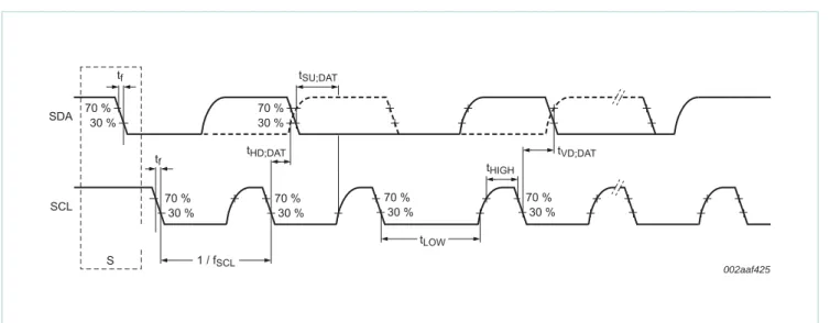
8.12.1.1 Features


![Table 13. Dynamic characteristic: I/O pins [1]](https://thumb-us.123doks.com/thumbv2/123dok_us/9565438.2441849/57.892.226.818.390.704/table-dynamic-characteristic-i-o-pins.webp)