Simply Adjustable Sinusoidal Oscillator
Based on Negative Three-Port Current Conveyors
Roman ŠOTNER
1, Zdeněk HRUBOŠ
1, Josef SLEZÁK
1, Tomáš DOSTÁL
21Dept. of Radio Electronics, Brno University of Technology, Purkynova 118, 612 00 Brno, Czech Republic 2Dept. of Electronics and Informatics, College of Polytechnics Jihlava, Tolsteho 16, Jihlava 586 01, Czech Republic
[email protected], [email protected], [email protected], [email protected]
Abstract. The paper deals with sinusoidal oscillator em-ploying two controlled second-generation negative-current conveyors and two capacitors. The proposed oscillator has a simple circuit configuration. Electronic (voltage) ad-justing of the oscillation frequency and condition of oscil-lation are possible. The presented circuit is verified in PSpice utilizing macro models of commercially available negative current conveyors. The circuit is also verified by experimental measurements. Important characteristics and drawbacks of the proposed circuit and influences of real active elements in the designed circuit are discussed in detail.
Keywords
Current conveyors, electronic adjusting, sinusoidal oscillator.
1.
Introduction
Many modern active functional blocks are available for application in analog technology and signal processing in the present time. This fact is discussed in paper [1] where the review and basic theory of the novel blocks are given. First applications of these blocks have been given in the literature, namely DBTA in [2], CFTA in [3] and others. An attention is now focused on the applications in current mode (CM) [4], in particular using the functional blocks with multi current outputs. There are some various modifications of the known circuit elements, namely the current conveyors (CC), the current feedback amplifiers (CFA) and the transconductors (OTA) with new names such as DO-CCCII [5 - 7], MO-CCII [8], CC-CFA [9], MO-OTA [10], or CDTA [11], [12], [13], CDBA [14] etc [1]. Because of their better frequency characteristics and features for electronic controlling, these blocks may be used in wide range of applications in the fields of filters, oscillators, high-speed communication systems, acoustic, measuring, control, sensor, and automotive electronics.
Recently, many circuits and concepts of harmonic oscillators based on CC of second generation (CCII) [15 -
31] and CFA [32 - 37] have been published. Many of these applications are not tunable [12, 13, 19, 22 and 23]. Others can be tuned by a single passive element, namely by a grounded resistor [15-18, 20, 27, 28, 30-32, 34-36, 38] or by a floating resistor [14, 21, 24, 31, 33-35, 37]. The grounded variable resistor can be simply implemented by a JFET [29, 34-35], by an OTA [39] or by a digital potenti-ometer. However using of the floating element is quite complicated, as you can see for example in a special filter in [40]. In several works [25-27] biasing current (Ib), which
drives the resistance Rx of the terminal X of the CC, is used
for electronic control. Unfortunately the parameter (Ib or Rx) depends on the IC manufacturing deviations, supply
voltage and also obviously on the temperature. Therefore it can cause some problems with precision in this application. Note that the manufacturing tolerances of the Rx can be
tens of percent.
Recently published circuits with the conveyors CCII are based on one active block only [21, 24, 31, 33, 36-38], complemented by four or five passive elements. Further-more circuits with two active blocks, complemented by four or six passive elements [13-14, 17, 19-20, 22, 25-27, 29, 32, 34, 36] and at the most with three CCII and eight passive elements [15-16, 19, 23, 28, 30, 34, 36] have been published. The positive-current conveyors or combination with negative ones are used in publications above. Note that the circuits mentioned above were mostly verified through simulations at audio frequencies only where the use of these new high-speed blocks is not substantiated. In audio band a classical VM approach, the standard opera-tional amplifiers and digital potentiometers for tuning can be fully sufficient. This is not suitable at higher frequen-cies, where parasitic capacitances and real parameters of the blocks play more significant role. Another weakness of the previous approaches can be inability of direct elec-tronic controlling (except controlling Rx for CCII),
compli-cated implementation (too many blocks and elements), low level of the output signal [24-25] and high THD [26, 34-35, 37].
In this paper very simple oscillator employing two negative conveyors CCII- is presented. Oscillation fre-quency and condition of oscillation may be driven varying electronically controlled current gains B. A basic variant
includes four passive components (two R and two C). Also resistor-less variant with two capacitors only is given. Here, instead of the real resistor, the input resistance Rx of
the conveyor terminal X (Fig. 1) is used. Note that the manufacturer guarantees the value of Rx in tolerance of
±20% so this must be taken into account during the design of this simpler variant. The output signal can be taken from two internal nodes. However, to separate the load imped-ance a voltage follower can be appropriately used.
On the other hand, the disadvantage of this circuit is that one working capacitor is floating and the oscillation frequency may be driven only in a limited range. Despite this, implementation of the proposed circuit is simpler comparing to previous oscillators discussed above. More current outputs are not required and a classical three-port CC is sufficient.
a) b)
Fig. 1. Principle of adjustable CCII-: a) Symbol, b) model.
2.
Three-Port Current Conveyor with
Adjustable Current Gain
The principle of this block is clear from Fig. 1. The negative three-port current conveyor CCII- with adjustable current gain has the symbol shown in Fig. 1a, where the port variables are denoted. This block can be described in a classical way [1]. The important relations are written in this figure, too. There is current input X, voltage input Y and current output Z. Compared to common types of the CCII (e.g. AD 844 [41]) this conveyor has the possibility of electronic controlling of the current gain B.
For design and verification, commercially available CCII- (obsolete but sufficient for experiments) was used. There is not a problem for layout designer to create similar element in CMOS or bipolar technology if necessary. This device is commercially available as EL 2082 as two-quad-rant current-mode multiplier [42]. The gain control input is calibrated to 1 mA/ mA signal gain (B) for 1 V of control voltage Vg (see [42]), else B = f(Vg) and simplification is
valid approximately (example: Vg = 2 V means that exactly B = 1.9). Features of this block are evident from following figures obtained through simulations in PSpice. Magnitude responses of the current gain B(f) are given in Fig. 2. The bandwidth (-3 dB) is 158 MHz for B0 = 1 = 0 dB. Varying
of B = B(f, Vg) by driving voltage Vg is also shown in
Fig. 2. Frequency 100Hz 10KHz 1.0MHz 100MHz 10Hz DB(I(R1)/I(I1)) -20 -10 -0 10 Vg = 2 V Vg = 1.5 V Vg = 1 V Vg = 0.5 V Vg = 0.1 V
Fig. 2. Magnitude response as a function of driving voltage B =B(f, Vg).
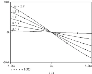
Input-output characteristics for several values of the driving voltage Iz =f (Ix, Vg) are shown in Fig. 3.
I_I1 -5.0mA 0A 5.0mA I(R1) -10mA 0A 10mA 0.1 V 0.5 V 1 V 1.5 V Vg = 2 V
Fig. 3. Input-output current characteristics Iz =f (Ix, Vg).
3.
Proposed Oscillator
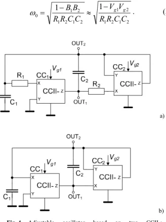
The proposed tunable oscillator employing two nega-tive conveyors CCII- is shown in Fig. 4. The basic variant (Fig. 4a) has four passive elements, two R and two C. In Fig. 4b, the resistor-less version is shown, using the input X resistance (Rx in Fig. 1) of the real conveyor.
The circuit from Fig. 4 has the characteristic equation of the second-order general form
0 0 1 2 2s a sa a . (1)
By symbolical nodal analysis, using the computer tool SNAP and setting of det Y = 0, the following characteristic equation is obtained 0 1 ) 1 ( 2 1 2 1 2 1 2 1 2 1 1 2 2 1 1 2 C C R R B B s C C R R B R C R C s . (2)
From the characteristic equation (2) we can determine the oscillation condition in the following form
1 2 2 2 2 1 1R C R C R B C , (3) 1 1 Vg B , (4)
and also the formula for the frequency of oscillations
2 1 2 1 2 1 2 1 2 1 2 1 0 1 1 C C R R V V C C R R B B g g
. (5) a) b)Fig. 4. Adjustable oscillator based on two CCII-:
a) basic variant, b) resistor-less variant.
The sensitivities of the oscillation frequency (5) to the passive components and parameters of the CC’s were found, namely 2 1 0 2 0 1 0 2 0 1 R R C C S S S S , (6) 2 1 0 2 0 1 x x R R S S , (7)
1 2
2 1 2 1 2 1 1 2 1 1 2 1 0 2 0 1 g g g g B B V V V V B B B B S S . (8)From (3) and (5) it is clear that B1 is not suitable for
0 control because it is also in the condition of oscillation
(3). However, B2 is only in (5) therefore it can be
theoreti-cally suitable for 0 control. The resistance R1 in formulas
above (also R2 by analogy) is given by the sum R1 = R1ext+ Rx1. External working resistor R1ext must be
added to Rx1, whichis the input of the current port X. Note
that these virtual resistances (Rx1, Rx2) (without R1ext, R2 ext)
are considered only in the resistor-less version (Fig. 4b). However, this utilization can be problematic due to the reason (Rx) discussed in the introductory section. The
product B1B2 above (respective Vg1Vg2) must be in range
0 ≤B1B2 < 1, which is a defining condition for the
operation of this circuit as an oscillator. Equation (8)
shows that sensitivities of oscillation frequency on parameters of active elements (current gain B) are quite high for B1B2→ 1 (Fig. 5) or B2→ 0.5 whereas B1= 2
respectively (see sections 4 and 5).
0 0.1 0.2 0.3 0.4 0.5 0.6 0.7 0.8 0.9 1 -50 -45 -40 -35 -30 -25 -20 -15 -10 -5 0 B1*B2 S en sit iv ity
Fig. 5. Detailed analysis of sensitivity (8) of oscillation frequency on product B1B2.
4.
Design Assumptions
The values of the capacitors are chosen C1= C2 =
= 470 pF, and the external resistors R1ext = R2ext = 100 Ω.
Then considering the virtual resistances Rx = 95 Ωthe total
values result in R1 = R2 = 195 Ω. The current gain B1 is
chosen B1 = 2 (then Vg1 ≈ 2 V) and B2 will be changed
tak-ing into account the oscillation condition above. The ex-pected value of the oscillation frequency estimated by (5) is f0 = 1.737 MHz (B2 = 0).
5.
Experimental Verification
To verify the proposed oscillator the simulations in PSpice using an adequate model of the real CCII- have been carried out. Fig. 6 shows the time waveforms of the output signals in both nodes denoted in circuit diagram (Fig. 4).
Time
74.00us 74.40us 74.80us 75.20us 75.60us
73.70us
V(out1) V(out2)
-1.0V 0V 1.0V
Fig. 6. Time waveforms of the output signals (for Vg1 = 2 V,
Vg2 = 0 V), given by simulation (transient analysis in PSpice).
Spectrum of the output signal resulting from the simulation using PSpice is given in Fig. 7.
Frequency 0Hz 2MHz 4MHz 6MHz 8MHz 10MHz 12MHz 14MHz 16MHz Vdb(out1) Vdb(out2) -60 -40 -20 -0
Fig. 7. Spectrum of the output signal.
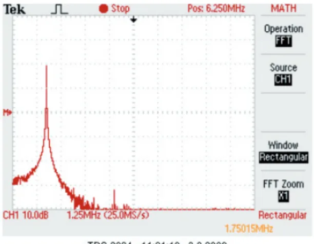
The simulations were supplemented by adequate labo-ratory measurements, as shown in Fig. 8 and Fig. 9. These results are confirmation of the theoretical and designed assumptions and also symbolical analysis given above.
Fig. 8. Measured output signals (larger is VOUT1, smaller is
VOUT2 for Vg1 = 2 V, Vg2 = 0 V)
Fig. 9. Measured spectrum of the output signal.
For start of the oscillations it was necessary to change the value of the R1 to 67 Ω, which caused changing of the
expected theoretical value of the oscillation frequency (f0)
to 1.9 MHz (instead of 1.7 MHz). The parasitic properties of active elements (Rx and their different values given by
manufacturing tolerance) causes that condition of oscilla-tion is not fulfilled. Although the influence of parasitic real features is discussed in the next chapter in detail, let's mention, that with regard to the parasitic features of the active blocks, the oscillation frequency is changed to 1.8 MHz, which was confirmed with the simulation by the macro models from [42]. The value of the f0 measured in
laboratory was still about 50 kHz lower (1.75 MHz). The dependence of the oscillation frequency f0 on the
control voltage Vg2 is shown in Fig 10, namely ideal
theo-retical, PSpice simulation, Matlab (version 7.6.0) calcula-tion and measured, too. The measurement of the output voltages (VOUT1 and VOUT2) versus the oscillation frequency
(f0) is resulting in the Fig 11. Similarly, the measuring of
dependence of the THD on the oscillation frequency f0 is
given in Fig 12. 0,0E+00 2,0E+05 4,0E+05 6,0E+05 8,0E+05 1,0E+06 1,2E+06 1,4E+06 1,6E+06 1,8E+06 2,0E+06 0,0 0,1 0,2 0,3 0,4 0,5 Vg2 [V] f0 [Hz]
ideal (theoretical) Matlab calculation PSpice simulation Measurement Fig. 10. Oscillation frequency versus control voltage.
0 0,2 0,4 0,6 0,8 1 1,2 1,4 1,6 1,8 2
0,0E+00 5,0E+05 1,0E+06 1,5E+06 2,0E+06
f0 [Hz]
Vout1,2 [Vp-p]
VCC = ± 5 V
VOUT1
VOUT2
Fig. 11. Output voltages vs. oscillation frequency (measured).
The maximal tunable frequency range is from 0.32 to 1.75 MHz (Vg2 from 0 to 0.48 V). Nevertheless, we can see
(Fig. 11 and Fig. 12) that for the minimal THD it is accept-able to work with the control voltage Vg2 from 0 to about
0.3 V (THD is below 1%). It reduces tuning to half range (approximately from 1 MHz to 1.75 MHz). There lower THD was achieved due to the internal nonlinearity of used active elements. In a wider range, it is necessary to add
a circuit for amplitude stabilization. The first approach contained CC1 with a fixed gain. Practically, in this case
we can obtain an invariable output magnitude in the total range of f0 but THD is incredible and output waveform
even limited. The CC1 with an adjustable gain is better for
direct controlling of the condition of oscillation but it affects a little bit also oscillation frequency (5) and output magnitude. It is appropriate for external amplitude stabili-zation. For keeping output amplitudes in less invariable level (Fig. 11) it was necessary to set Vg1 in every
meas-ured point (only very small change, see Tab. 1), but THD increased when Vg2 was above 0.3 V. In other case (Vg1
was fixed) the amplitudes varied for example from 0.5 to 1 Vp-p (VOUT2) but THD was still under 1%. In the rest of
theoretical range (approximately from 0.35 to 0.5 V) it is important to set Vg1 in each next measured point otherwise
THD is very high. These corresponding results are in Tab. 1. 0 1 2 3 4 5 6 7 8 9 10
0,0E+00 5,0E+05 1,0E+06 1,5E+06 2,0E+06
f0 [Hz]
THD[%] VCC = ± 5 V
Fig. 12. THD versus oscillation frequency (measured).
f0 [MHz] Vg1 [V] Vg2 [V] Separation of higher harmonics [dB] THD [%] 0.32 2.06 0.48 20 9.9 0.51 2.05 0.45 30 2.1 0.77 2.02 0.40 35 1.8 0.91 2.01 0.35 38 1.3 1.10 1.98 0.30 45 0.6 1.36 1.97 0.20 47 0.5 1.60 1.95 0.10 48 0.4 1.68 1.94 0.05 51 0.3 1.75 1.93 0 50 0.3
Tab. 1. Values of Vg1 and Vg2 and THD for different measured oscillation frequencies.
6.
Parasitic Influences
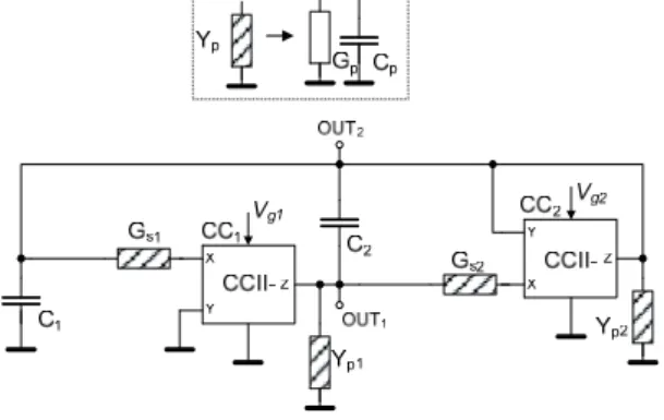
In Fig. 13 the suitable model of the real CCII- which includes the most important parasitic parameters is given. Then using this model (Fig. 13) the circuit diagram from Fig. 4 can be supplemented as shown in Fig. 14 to include all parasitic influences of the practical oscillator. Elements
with crosshatch pattern are representing parasitic influ-ences.
Fig. 13. Important parasitic influences of CCII-.
Fig. 14. Important parasitic influences in the proposed oscil-lator.
This circuit (Fig. 14) has the characteristic equation in the polynomial form (1) with the coefficients in symbolical form as follows: 1 2 a , (9) 2 1 2 1 2 2 2 1 1 1 2 2 1 2 1 2 * 1 1 2 1 1 2 1 2 1 2 2 2 1 1 1 2 2 1 2 1 * 2 2 2 1 2 1 2 2 2 1 1 1 1 2 1 1 2 1 1 C C C C C C C C C C C C G C G C B G C G C C C C C C C C C C C C G C G C B G C C C C C C C C C C G C C G G C a p p p p p p p p s s p p p p p p p s p p p s p p p p p p p s s , (10)
2 1 2 1 2 2 2 1 1 1 * 2 1 2 1 1 2 2 2 1 2 1 * 2 * 1 0 1 C C C C C C C C C C B G G G G G G G G G G B B a p p p p p p s p s p s p p s s (11) In formulas (10) and (11) the following symbols represent the parasitic influences: 1/ 1 1 1 1 1 95 20% 1 s ext x x ext s G R R R R R , (12) 1/ 2 2 2 2 2 95 20% 2 s ext x x ext s G R R R R R , (13) 1 1 1/ z p R G , (14) 2 2 2 1/ z 1/ y p R R G , (15) 1 1 z p C C , (16)
2 2 2 z y p C C C , (17) T T s B B 1 * 1 , T T s B B 2 * 2 . (18), (19)
Analyzing the equations above, one can see that the influence of the resistance Rp = 1/Gp begins to show
symptom in slight increasing of the oscillation frequency f0
for Rp less than 50 kΩ (but the employed blocks allow to
achieve several higher values). Note that the influence of the Rp1 is only slightly larger than Rp2. On the other hand
the capacitances Cp play more significant role. Only small
change of the capacitance results in a significant change of
f0 (e.g. for both Cp = 5 pF it is over 20 kHz). The influence
of the Cp2 is greater than Cp1 due to their values,
approxi-mately Cp1 = 5 pF and Cp2 = 7 pF. This is due to the fact
that the parasitic capacitance Cy plays also role but not in
CC1 (port Y is grounded). Furthermore inequality of the
input resistances of the current ports Rx1≠Rx2 plays a
sig-nificant role, too. Their values are determined by tech-nology and have high production tolerance.
The results obtained by direct analysis of the model (Fig 14) respecting essential parasitic influences in the real oscillator are in a very good accordance with the computer simulations and obtained experimental results. Due to the relatively high tolerance of the resistances Rx, the
differ-ence between the theoretically assumed value and the measurement is greater than the difference between the computer simulation and the direct analysis of the model above.
7.
Conclusion
In this paper very simple electronically adjustable oscillator employing only two active devices (CCII-) and in the extreme only two passive elements (capacitors) was presented. It allows electronic tuning of the oscillation frequency and condition of oscillation by DC driving volt-age. It was practically tested from 320 kHz to 1.75 MHz. Under certain conditions (limited range), the harmonic distortion can be achieved below 1% and the separation of the higher harmonics more then 50 dB. However there are some drawbacks of this solution. The equation for oscilla-tion frequency (5) is not very suitable and therefore tuning is possible only in a limited range. The topic of future work will be focused on removing of this drawback. The circuit was verified without the circuit for amplitude stabilization (only by nonlinear limitation of used active elements). Therefore practically available range of tuning with achievable low THD is restricted. For invariable level of output signal very small changes of B1 are necessary. The
first conception of the oscillator where CC1 has a fixed
gain is not suitable because the control of the condition of oscillation is not possible. Operation of the proposed oscillator was verified through simulations and measure-ments of the real circuit in the frequency range of units MHz. Also important parasitic effects in this circuit were
discussed in detail. The oscillator was analyzed symboli-cally, tested by computer simulations and by laboratory experiments. This allows a comprehensive view of the behavior of this circuit. The designed circuit will be used for education purposes in courses dealing with electroni-cally adjustable active elements and their applications.
Acknowledgements
The authors are thankful to the editors and reviewers for their constructive recommendations, which helped to improve this paper. The research described in the paper was supported by the Czech Ministry of Education under research program MSM 0021630513 and Czech Science Foundation projects under No. 102/08/H027 and No. 102/09/1681. Research described in the paper is a part of the COST Action IC0803 RF/Microwave communication subsystems for emerging wireless technologies, financed by the Czech Ministry of Education by the grant no. OC09016.
References
[1] BIOLEK, D., SENANI, R., BIOLKOVA, V., KOLKA, Z. Active elements for analog signal processing: Classification, Review, and New Proposal. Radioengineering, 2008, vol. 17, no. 4, pp. 15 – 32. [2] HERENCSAR, N., VRBA, K., KOTON, J., LATTENBERG, I.
The conception of differential-input buffered and transconductance amplifier (DBTA) and its application. IEICE Electronics Express,
2009, vol. 6, no. 6, pp. 329-334.
[3] HERENCSAR, N., KOTON, J., VRBA, K., MISUREC, J. A novel current-mode SIMO type universal filter using CFTAs.
Contemporary Engineering Sciences, 2009, vol. 2, no. 2, pp. 59 to 66.
[4] TOUMAZOU, C., LIDGEY, F. J., HAIGH, D. G. Analogue IC Design: The Current Mode Approach. London: Peter Peregrinus Ltd., 1990.
[5] TANGSRIRAT, W. Current-tunable current-mode multifunctional filter based on dual-output current-controlled conveyors. AEU – International Journal of Electronics and Communications, 2007, vol. 61, no. 8, pp. 528-533.
[6] JAIKLA, W., SIRIPRUCHYANUN, M. Low-component elec-tronically controllable dual-mode universal biquad filter using DO-CCCIIs. In Proceedings of Asia-Pacific Conference on Communications 2007, pp. 331-334.
[7] BIOLEK, D., SIRIPRUCHYANUN, M., JAIKLA, W. CCII and OTA based current-mode universal biquadratic filter. In The Sixth PSU Engineering Conference, May 2008, pp. 238-241.
[8] WANG. C, ZHAO, Y., ZHANG, Q., DU, S. A new current mode SIMO-type universal biquad employing multi-output current conveyors (MOCCIIs). Radioengineering, 2008, vol. 18, no. 1, pp. 83–88.
[9] SIRIPRUCHYANUN, M., CHANAPROMMA, C., SILAPAN, P., JAIKLA, W. BiCMOS current-controlled current feedback amplifier (CC-CFA) and its applications. WSEAS Transactions on Electronics, 2008, vol. 5, no. 6, pp. 203-219.
[10] BIOLEK, D., BIOLKOVA, V., KOLKA, Z. Universal current-mode OTA-C KHN biquad. International Journal of Electronics, Circuits and Systems, 2007, vol. 1, no. 4, pp. 214-217.
[11] KESKIN, A. U., BIOLEK, D., HANCIOGLU, E., BIOLKOVA, V. Current-mode KHN filter employing current differencing transconductance amplifiers. Int. J. Electronics and Communications, 2006, vol. 60, no. 6, pp. 443-446.
[12] BIOLEK, D., BIOLKOVA, V., KESKIN, A. U. Current mode quadrature oscillator using two CDTAs and two capacitors. In
Proceedings of the 5th Int. Conf. on System Science and Simulation
in Engineering. Spain, 2006, pp. 368-370.
[13] LAHIRI, A. New current-mode quadrature oscillators using CDTA. IEICE Electronics Express, 2009, vol. 6, no. 3, pp. 135 to 140.
[14] MAHESHWARI, S., KHAN, I. A. Novel single resistor controlled quadrature oscillator using two CDBAs. Journal of Active and Passive Electronic Devices, 2007, vol. 2, pp. 137-142.
[15] HORNG, J. W. Current conveyors based allpass filters and quadrature oscillators employing grounded capacitors and resistors. Computers and Electrical Engineering, 2005, vol. 31, pp. 81-92.
[16] CHANG, C. M. Novel current-conveyor-based single-resistance-controlled/voltage-controlled oscillator employing grounded resistors and capacitors. Electronic Letters, 1994, vol. 30, no. 3, pp. 181-183.
[17] KUMAR, V., PAL, K. Single element controlled sinusoidal oscillators using current conveyors. Journal of Active and Passive Electronic Devices, 2009, vol. 8. pp. 197-202.
[18] KUMAR, A., VYAS, A. L. A single resistance controlled eight possible oscillator circuits for analog signal processing applications. Academic Open Internet Journal, 2007, vol. 21, pp. 1-7.
[19] TOKER, A., KUNTMAN, H., CICEKOGLU, O., DISCIGIL, M. New oscillator topologies using inverting second-generation current conveyors. Turk. J. Elec. Engin., 2002, vol. 10, no. 1, pp. 119-129.
[20] SHEN-IUAN, LIU. Single-resistance-controlled/voltage controlled oscillator using current conveyors and grounded capacitors.
Electronic Letters, 1995, vol. 31, no. 5, pp. 337-338.
[21] AGGARWAL, V. Novel canonic current mode DDCC based SRCO synthesized using a genetic algorithm. Analog Integrated Circuits and Signal Processing, 2004, vol. 40, pp. 83-85.
[22] SOLIMAN, A. M. Current-mode oscillators using single output current conveyors. Microelectronics Journal, 1998, vol. 29, pp. 907-912.
[23] SOLIMAN, A. M. Synthesis of grounded capacitor and grounded resistor oscillators. Journal of the Franklin Institute, 1999, vol. 336, pp. 735-746.
[24] LAHIRI, A. Additional realization of single-element-controlled oscillators using single ICCII-. International Journal of Computer and Electrical Engineering, 2009, vol. 1, no. 3, pp. 303-306. [25] PANDEY, N., PAUL, K. A novel electronically tunable sinusoidal
oscillator based on CCCII (-IR). Journal of Active and Passive Electronic Devices, 2008, vol. 3, pp. 135-141.
[26] HORNG, J. W. A sinusoidal oscillator using current-controlled current conveyors. Int. Journal of Electronics, 2001, vol. 88, no. 6, pp. 659-664.
[27] HORNG, J. W., LIN, S., YANG, CH. Sinusoidal oscillators using current conveyors and grounded capacitors. Journal of Active and Passive Electronic Devices, 2007, vol. 2, pp. 127-136.
[28] ABUELMAATTI, M. T. New sinusoidal oscillators with fully uncoupled control of oscillation frequency and condition using three CCII+s. Analog Integrated Circuits and Signal Processing, 2000, vol. 24, pp. 253-261.
[29] KHAN, A. A., BIMAL, S., DEY, K. K., ROY, S. S. Novel RC sinusoidal oscillator using second-generation current conveyor.
IEEE Transaction on Instrumentation and Measurement, 2005, vol. 54, no. 6, pp. 2402-2406.
[30] MARTINEZ, P. A., SABADELL, J., ALDEA, C., CELMA, S. Variable frequency sinusoidal oscillators based on CCII+. IEEE Transaction on Circuits and Systems-I: Fundamental Theory and Applications, 1999, vol. 46, no. 11, pp. 1386-1390.
[31] KILINC, S., JAIN, V., AGGARWAL, V., CAM, U. Catalogue of variable frequency and single-resistance-controlled oscillators employing a single differential difference complementary current conveyor. Frequenz, 2006, vol. 60, no. 7-8, pp. 142-146.
[32] SHEN-IUAN, LIU, JIANN-HORNG, TSAY Single-resistance-controlled sinusoidal oscillator using current-feedback-amplifiers.
Int. Journal of Electronics, 1996, vol. 80, no. 5, pp. 661-664. [33] SHEN-IUAN, LIU, CHUNG-SHINN, Shih., DONG-SHIUH, Wu.
Sinusoidal oscillators with single element control using a current-feedback amplifier. Int. Journal of Electronics, 1994, vol. 77, no. 6, pp. 1007-1013.
[34] GUPTA, S. S., BHASKAR, D. R., SENANI, R. New voltage controlled oscillators using CFOAs. AEU – Int. J. of Electronics and Communications, 2009, vol. 63, no. 3, pp. 209-217.
[35] BHASKAR, D. R., SENANI, R. New CFOA-based single-element-controlled sinusoidal oscillators. IEEE Transaction on Instrumentation and Measurement, 2006, vol. 55, no. 6, pp. 2014 to 2021.
[36] SOLIMAN, A. M. Current feedback operational amplifier based oscillators. Analog Integrated Circuits and Signal Processing, 2000, vol. 23, no. 1, pp. 45-55.
[37] SINGH, V. K., SHARMA, R. K., SINGH, A. K., BHASKAR, D. R., SENANI, R. Two new canonic single-CFOA oscillators with single resistor controls. IEEE Transaction on Circuits and Systems-II: Express Briefs, 2005, vol. 52, no. 12, pp. 860-864. [38] CAM, U., TOKER, A., CICEKOGLU, O., KUNTMAN, H.
Current-mode high output impedance sinusoidal oscillator configuration employing single FTFN. Analog Integrated Circuits and Signal Processing, 2000, vol. 24, pp. 231-238.
[39] RANDALL, L. G., SANCHEZ-SINENCIO, E. Active filter design using operational transconductance amplifiers: A tutorial. IEEE Circuits and Devices Magazine, 1985, vol. 1, pp. 20-32.
[40] DOSTAL, T., AXMAN, V. Biquads based on single negative impedance converter implemented by classical current conveyor.
Radioengineering, 2007, vol. 16, no. 3, pp. 96-102.
[41] Analog Devices. Monolithic Op Amp AD 844, 16 p. [Online] Available at: http://www.analog.com
[42] Intersil (Elantec). EL 2082CN Current-Mode Multiplier, 1996, 16 p. [Online] Available at: http://www.intersil.com
About Authors ...
Roman ŠOTNER was born in Znojmo, Czech Republic,
in 1983. He received the MSc. degree (2008) from the Brno University of Technology. Currently he is Ph.D. student at the Faculty of Electrical Engineering and Com-munication. His interests are analog circuits (active filters,
oscillators, audio, etc.), circuits in the current mode and computer simulation.
Zdenek HRUBOŠ was born in Uherske Hradiste, Czech Republic, in 1984. He received his MSc. degree in 2009 from the University of Technology, Brno. He is currently studying his Ph.D. study at the same university. His research interest is in computer analysis and synthesis of electronics circuits and nonlinear systems.
Josef SLEZÁK was born in Zlin, Czech Republic, in 1982. He received his MSc. degree in 2007 from the Uni-versity of Technology, Brno. He is currently studying his Ph.D. study at the same university. His research interest is
in analysis and design of analog circuits operating in cur-rent mode.
Tomáš DOSTÁL (*1943) received his Ph.D. (1976) and Dr.Sc. degree (1989). He was with the University of De-fense Brno (1976-1978 and 1980-1984), with the Military Technical College Baghdad (1978-1980), with the Brno University of Technology (1984-2008) and with the Euro-pean Polytechnic Institute (2008 - 2009). Since 2009 he has been with the College of Polytechnics, Jihlava as Pro-fessor of Electronics. His interests are in circuit theory, analog filters, switched capacitor networks and circuits in the current mode.
R
ADIOENGINEERING
R
EVIEWERS
September 2010, Volume 19, Number 3
ARCE-DIEGO, J. L., University of Cantabria, Santander, Spain
BALLING, P., Antenna Systems Consulting ApS, Denmark
BEČVÁŘ, Z., Czech Technical University in Prague, Czechia
BEŠŤÁK, R., Czech Technical University in Prague, Czechia
BEZPALEC, P., Czech Technical University in Prague, Czechia
BIOLEK, D., University of Defense, Brno, Czechia
BONEFAČIĆ, D., University of Zagreb, Croatia
BRANČÍK, L., Brno University of Technology, Czechia
ČERNOCKÝ, J., Brno University of Technology, Czechia
ČERNÝ, P., Czech Technical University in Prague, Czechia
DOBEŠ, J., Czech Technical University in Prague, Czechia
DORDOVÁ, L., Brno University of Technology, Czechia
DŘÍNOVSKÝ, J., Brno University of Technology, Czechia
ELHADJ, Z., University of Tébéssa, Algeria
FEDRA, Z., Brno University of Technology, Czechia
FLIEGEL, K., Czech Technical University in Prague, Czechia
FONTAN, P. F., University of Vigo, Spain
FRÝZA, T., Brno University of Technology, Czechia
GALAJDA, P., Technical University of Košice, Slovakia
GEORGIADIS, A., Centre Tecnologic de
Telecomunicacions de Catalunya, Barcelona, Spain
GRÉZL, F., Brno University of Technology, Czechia
GRGIĆ, M., University of Zagreb, Croatia
HAJNÝ, J., Brno University of Technology, Czechia
HANUS, S., Brno University of Technology, Czechia
HAZDRA, P., Czech Technical University in Prague, Czechia
HÁJEK, K., University of Defense, Brno, Czechia
HEROUT, A., Brno University of Technology, Czechia
HONZÁTKO, P., Academy of Sciences of the Czech Republic, Prague, Czechia
HORSKÝ, P., AMIS Czech, Ltd., Brno, Czechia
HOSPODKA, J., Czech Technical University in Prague, Czechia
HOZMAN, J., Czech Technical University in Prague, Czechia
KESKIN, A. U., Yeditepe University, Istanbul, Turkey
KLÍMA, M., Czech Technical University in Prague, Czechia
KOLKA, Z., Brno University of Technology, Czechia
KOUDELKA, V., Brno University of Technology, Czechia
KOLÁŘ, R., Brno University of Technology, Czechia
KOVÁŘ, P., Czech Technical University in Prague, Czechia
KULLA, P., Slovak University of Technology, Bratislava, Slovakia
KVIČERA, M., Czech Technical University in Prague, Czechia
LÁČÍK, J., Brno University of Technology, Czechia
LEONE, M., Otto-von-Guericke-Universitat, Magdeburg, Germany
LUKEŠ, Z., Brno University of Technology, Czechia
MACHÁČ, J., Czech Technical University in Prague, Czechia
MACI, S., University of Siena, Italy
MARŠÁLEK, R., Brno University of Technology, Czechia
MARTINEZ-VAZQUEZ, M., IMST GmbH, Kamp-Lintfort, Germany
MARTÍNEK, P., Czech Technical University in Prague, Czechia
MEHLFÜHRER, C., Vienna University of Technology, Austria
NOVOTNÝ, V., Brno University of Technology, Czechia
PÁTA, P., Czech Technical University in Prague, Czechia
PETRŽELA, J., Brno University of Technology, Czechia
POKORNÝ, M., Brno University of Technology, Czechia
POLÍVKA, M., Czech Technical University in Prague, Czechia
PROKOPEC, J., Brno University of Technology, Czechia
PUSKELY, J., Brno University of Technology, Czechia
RAIDA, Z., Brno University of Technology, Czechia
RIDZOŇ, R., Technical University of Košice, Slovakia
RUPP, M., Vienna University of Technology, Austria
ŘÍHA, K., Brno University of Technology, Czechia
SEGOVIA-VARGAS, D., Carlos III University of Madrid, Spain
SIGMUND, M., Brno University of Technology, Czechia
SIZOV, V., University of Birmingham, UK
SLANINA, M., Brno University of Technology, Czechia
SLEZÁK, J., Brno University of Technology, Czechia
SMÉKAL, Z., Brno University of Technology, Czechia
SZABÓ, Z., Czech Technical University in Prague, Czechia
SYSEL, P., Brno University of Technology, Czechia
ŠEBESTA, J., Brno University of Technology, Czechia
ŠEBESTA, V., Brno University of Technology, Czechia
ŠIMKO, M., Vienna University of Technology, Austria
ŠOTNER, R., Brno University of Technology, Czechia
ŠVIHLÍK, J., Institute of Chemical Technology in Prague, Czechia
TOŠOVSKÝ, P., Brno Univ. of Technology, Czechia
ULOVEC, K., Czech Technical University in Prague, Czechia
VALENTA, V., ESIEE Paris, France
VLČEK, Č., University of Defense, Brno, Czechia
WIESER, V., University of Žilina, Slovakia
YANNOPOULOU, N., Democritus University of Thrace, Greece
YILMAZ, A. E., Ankara University, Turkey
ZAPLATÍLEK, K., University of Defense, Brno, Czechia
ZIMOURTOPOULOS, P., Democritus University of Thrace, Greece