ISSN 2348 – 7968
Implementation and Analysis of Five-Level Buck Converter Open Loop
System for High Voltage Application
Manu.N.R1 and V.Nattarasu 2
1
M.Tech in Industrial Electronics, SJCE, Mysore-570006, [email protected],
2
Associate Professor, Dept. of ECE, SJCE, Mysore-570006, [email protected]
Abstract
The buck converter topology with higher voltage in the HVDC distribution system is a major challenge in the power converter implementation. The difficulty in implementation comes in the form of dv/dt loss across the switches, high voltage devices and high frequency operation. In order to get rid of these disadvantages the multilevel buck converter is introduced which because of the more number of switches in series reduces the voltage across each switch. The features of these converters are high gain, self balancing voltage, transformer less operation and reduced losses. The performance of the Five-Level Buck converter is analyzed by varying the designed value of inductor and capacitor by ±20%. The analysis of the simulation results are shows satisfactory performance of the converter. Matlab/simulink® has been used for computer simulation of the proposed Five-Level Buck converter under open loop condition.
Keywords: Buck, Converter, Losses, Ripple
1. Introduction
A nonisolated multilevel stepdown dc-dc converter suitable for high voltage application. The main features of this topology are: low voltage across the semiconductors;low switching losses and reduced volume of output filter[1].
The challenges and the opportunities associated with adopting the DC distribution scheme in the power systems, the issues like interaction between the power converters that are use to convert ac-dc and dc-ac and other challenging issue like proper grounding and neutral voltage shift are the major issues in the DC converter schemes[2]. Along with the increase in the capacity of offshore wind farms and the distance between the offshore wind farm and the land, the DC collection and the DC transmission grid, with the advantages such as reactive power and harmonics etc, becomes attractive under the growing trends of the offshore wind farm development[3-6].
The four switch full bridge dc to dc converter topology is basically for high input voltages, it gives one half of the input voltage across all the four switches, where in which
the two legs of the converter are connected in series with each other across the input. Due to this the switching losses across switch reduces[7].
The voltage stress on each of the switches in the multilevel converter is one third of the input voltage, and this can be obtained by soft switching method so that the switches are of low resistance and low voltage rating can be used [8-9]. And another common solution to reduce the voltage loss across switches are with series input and parallel output connections , where here the low voltage MOSFET switches are used, and its application is only for the medium voltage [10].
In order to achieve the high power, high voltage and high current semiconductor switches are required. Currently the IGCT with breakdown voltage of (6.9kV) is the most commonly used semiconductor for high voltage application, and also the IGBT with breakdown voltage of (6.5kV) are used. So in practice for high switching frequency operation (>10 kHz) the most attractive switches are IGBT and MOSFET [11-12].
Within these parameters, this paper presents a non isolated five level buck converter for high voltage application. The main features of this five level converter are: low harmonic distortion, low voltage stress across switches, low EMI noise, high efficiency, ability to operate without magnetic components. The detailed design of inductor and capacitor along with there current and voltage ripples, and the analysis of the Five-Level buck converter with ±20% variation in the designed inductor and capacitor values under open loop condition are presented here.
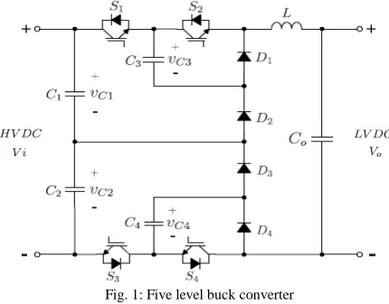
It may be necessary to change the number of capacitors connected in series in accordance with the input voltage of the converter. The voltage across the capacitors must be balanced for the safe operation of the proposed converter. Fig. 1 shows the five level buck converter.
ISSN 2348 – 7968 The topology of the five level buck converter is taken from
the flying capacitor multilevel inverters. Where they build the voltage levels by using the different levels of capacitors, the voltages of the capacitors add in each level resulting in increase in the voltage. But in the proposed converter it is the other way, it will decrease the voltage by the number of levels for each inclusion of the capacitor. Hence the topology acts as the buck converter.
Fig. 1: Five level buck converter
The analysis is performed considering the steady-state operation in continuous-conduction-mode of the five level Buck converter. The voltage over the semiconductors and the capacitors C3 and C4 is Vi/4, while the voltage across the capacitors C1 and C2 is Vi/2, where Vi is the input voltage.
The five level buck converter is operated in four operating regions. The waveforms for each operating region are shown and explained. The expression of static gain, inductor current ripple and the capacitor voltage ripple are derived.
2.1 Modulation strategy and main wave forms
The modulation strategy adopted here is based on phase-shift PWM, with 90 degree phase phase-shift between subsequent carriers. There are four carrier signals, and each carrier signal is used generate the gating pulse of one switch. And this technique allows the charging and discharging of each capacitor, and this implementation helps for active control of capacitor voltage balancing. The five level converter operated in four operating regions, and it is shown in below Table 1.
Fig. 2 shows the main wave forms (for the four operating regions) of the five level buck converter with switching period .
Table 1: Operating region of five level buck converter Duty-Cycle Output voltage
Limits
Operating regions
d < ¼ 0 - R1
¼ < d < ½ - R2
½ < d < ¾ - 3 R3
¾ < d < 1 3 - R4
Fig. 2. Main waveform of five level buck converter
From the Fig.2 it is observed that the proposed converter presents 16 switching states. And In Fig. 2 is the voltage before the low pass filter (LC section), and the average voltage across the inductor is given by equation(1) where the area under (t) over the time period is considered.
(1) (t) is the voltage across the inductor, that is
.
2.2 Static Gain
The steady state operation requires that the inductor current at the end of the switching cycle be the same as that at the beginning, meaning that the net change in the inductor current over one period is zero. Where the one switching period is .
(2) By considering that the converter is operating in region R1,
ISSN 2348 – 7968 expression of the static gain as a function of duty cycle D
is obtained as shown in equation (4). And it shows that static gain of the five level buck converter is same as that of conventional buck converter.
D = (4) 2.3 Inductor Current Ripple
By considering the energy storing or the energy transfer state of the inductor, the current ripple in the inductor can
be calculated and this expression is given in equation(5). (5) The time interval has different values depending on the operating region and it is obtained from Fig. 2.
The current ripple through the inductor has different behavior according to the operating region. So that equation (5) must be used for all operating regions of five level buck converter. Hence by changing the value of in all the operating regions we can get the current ripple equation for each operating region.
In region R1,
And putting ( )
(6. a)
In region R2,
(6. b)
In region R3,
(6. c)
In region R4,
(6. d)
The above equations 6. (a) (b) (c) & (d) gives the inductor current ripple in all four operating regions, where is the switching frequency.
The inductor current ripple in the fivel level buck converter reduces by 16 times. Further, from this the value of inductor can be given by equation (7).
L = (7)
2.4 Capacitors Voltage Ripple
Here in this section the voltage ripple across the capacitors C1, C2, C3 and C4 are analyzed. Voltage ripple can be calculated by considering the energy storing state or the energy transfer state of the capacitor and is given by equation (8).
(8) Where is the charge or discharge time interval and
is the instantaneous capacitor current. For the capacitor C1 and C2 the charge interval time is given
by ,
and . And the charging
current of these capacitors are = . By
substituting these values in equation(8) the voltage ripple across the capacitors C1 and C2 are obtained as shown in equation(9. a) & (9. b).
For capacitor ,
(9.a)
For capacitor ,
(9. b)
And likewise for the capacitors C3 and C4 the charge
interval time is given by, ;
; and
<D< 1. The charging current of these capacitors are iC(t) =IL, And by substituting these values in equation(8) the voltage ripple across the capacitors C3 and C4 are obtained as shown in equation(10. a), (10. b) & (10. c).
For capacitor ,
(10. a)
For capacitor ,
ISSN 2348 – 7968
(10. c) The maximum voltage ripple occurs for D = 0.5, for all capacitors, hence by assuming this maximum voltage ripple the capacitance expression can be derived as shown in below equation(11).
C = (11)
3. Experimental results
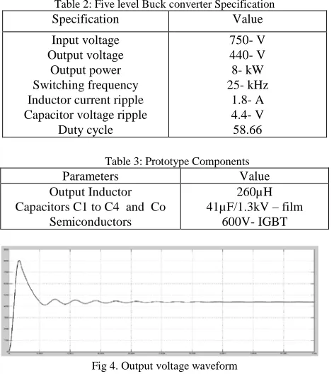
To verify the operation and evaluate the performance of the proposed five level Buck converters, an 8-kW prototype was design and the proposed topology was experimentally verified. The converter specifications are shown in Table 2. Due the relation of the input-output voltage, the converter operates in the region R3.The selected components are shown in Table 3. Fig. 3 shows the open loop simulation model of five level buck converter.
Table 2: Five level Buck converter Specification
Specification Value Input voltage
Output voltage Output power Switching frequency Inductor current ripple Capacitor voltage ripple
Duty cycle
750- V 440- V 8- kW 25- kHz
1.8- A 4.4- V 58.66
Table 3: Prototype Components
Parameters Value Output Inductor
Capacitors C1 to C4 and Co Semiconductors
260µH 41µF/1.3kV – film
600V- IGBT
Fig 4. Output voltage waveform
Performance analysis of five-level buck converter was carried out with ±20% variations from the designed value of the inductor and capacitor, by keeping one parameter constant at a time. The variation in peak over shoot, settling time, delay time, rise time and peak time for varied capacitor and inductor values were plotted. The below Table 4 shows the tabulation of different
parameter with constant capacitor value of 41μF and ±20%
variations from the designed value of inductor. Table 5 shows the tabulation of different parameters with constant inductor
value of 260μH and ±20% variations from the designed value of
the capacitor.
Fig. 3. Open loop Simulation model of five level buck converter
Fig 5. Output current waveform
Table 4: Variation of Parameter With Constant Capacitor Value
Inducto
r Value
In (µH) Over
Shoot
(Mp)
In
Volts
Settling
Time(ts)
In
Seconds
Delay
Time( )
In
Seconds
Rise
time(
In
seconds
Peak
time(
In
seconds
208 372.3 8.010e-3 9.535e-5 1.467e-4 2.925e-4
221 372.0 8.050e-3 9.830e-5 1.516e-4 3.001e-4
234 371.4 8.090e-3 1.012e-4 1.565e-4 3.050e-4
247 369.2 8.095e-3 1.040e-4 1.612e-4 3.100e-4
260 366.6 8.100e-3 1.069e-4 1.656e-4 3.172e-4
273 365.6 8.096e-3 1.098e-4 1.698e-4 3.340e-4
286 365.3 8.095e-3 1.126e-4 1.738e-4 3.413e-4
299 364.3 8.106e-3 1.155e-4 1.778e-4 3.453e-4
312 362.4 8.109e-3 1.181e-4 1.817e-4 3.491e-4
ISSN 2348 – 7968
Capacito
r Value
In (µF)
Over
Shoot
(Mp)
In
Volts
Settling
Time(ts)
In
Seconds
Delay
Time( )
In
Seconds
Rise
time(
In
seconds
Peak
time(
In
Seconds
33 359.5 8.087e-3 9.605e-5 1.484e-4 2.937e-4
35 362.9 8.088e-3 9.880e-5 1.529e-4 3.009e-4
37 365.2 8.094e-3 1.015e-4 1.573e-4 3.053e-4
39 366.2 8.120e-3 1.042e-4 1.616e-4 3.100e-4
41 366.6 8.150e-3 1.069e-4 1.656e-4 3.172e-4
43 368.4 8.175e-3 1.096e-4 1.694e-4 3.348e-4
45 370.8 8.180e-3 1.122e-4 1.731e-4 3.408e-4
47 372.5 8.220e-3 1.148e-4 1.767e-4 3.449e-4
49 373.3 8.240e-3 1.174e-4 1.802e-4 3.484e-4
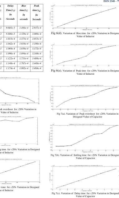
Fig 6(a). Variation of Peak overshoot for ±20% Variation in Designed Value of Inductor
Fig 6(b). Variation of settling time for ±20% Variation in Designed Value of Inductor
Fig 6(c). Variation of Delay time for ±20% Variation in Designed Value of Inductor
Fig 6(d). Variation of Rise time for ±20% Variation in Designed Value of Inductor
Fig 6(e). Variation of Peak time for ±20% Variation in Designed Value of Inductor
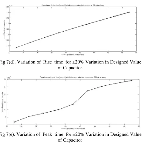
Fig 7(a). Variation of Peak overshoot for ±20% Variation in Designed Value of Capacitor
Fig 7(b). Variation of Settling time for ±20% Variation in Designed Value of Capacitor
ISSN 2348 – 7968
Fig 7(d). Variation of Rise time for ±20% Variation in Designed Value of Capacitor
Fig 7(e). Variation of Peak time for ±20% Variation in Designed Value of Capacitor
From Figures Fig 6. (a),(c),(d) and Fig 7. (a),(c),(d) the peak overshoot, delay time and Rise time varies linearly with changes in inductor and capacitor value. But it be observed that in the Fig 6. (b),(e) and Fig 7. (b),(e) due to the variation of inductance and capacitance there is a significant effect on the settling time and the peak time of the converter waveform.
4. Conclusions
A nonisolated five level Buck converter for high voltage application was proposed and structure was analyzed in detail in this paper. The advantages of this converter are absence of a transformer, a reduced number of components, a reduced volume of output filter and low voltage across the semiconductors.
The proposed converter is designed and simulated. The converter was designed to supply a load at 440V at 8000W with duty ratio of 0.586. The output waveforms obtained from simulations confirms the better performance of the proposed converter. Analysis are carried out by varying the ±20% of the capacitor and inductor designed value. Further future work will concentrate on designing the closed lopp controller for the efficient operation of the proposed converter.
References
1. F. Costa, S. A. Mussa and I. Barbi, “Multilevel buck dc-dc converter for high voltage application,”
Industry Applications (INDUSCON),2012 10th IEEE/IAS International Conference on Digital Object Identifier: Publication Year: 2012.
2. M. Baran and N. Mahajan, Dc distribution for industrial systems: opportunitiesand challenges,” IEEE Transactions
on Industry Applications, vol. 39, no. 6, pp. 1596– 1601, nov-dec. 2003.
3. O. Gomis-Bellmunt, A. Junyent-Ferre, A. Sumper, and J. Bergas-Jane, “Control of a wind farm based on synchronous generators with a central HVDC-VSC converter,” IEEE Transactions on Power System, vol. 26, no. 3, pp. 1632-1640, August 2011.
4. J. Robinson, D. Jovcic, and G. Joo ands, “Analysis and design of an offshore wind farm using a mv dc grid,” IEEE Transactions on Power Delivery, vol. 25, no. 4, pp. 2164 – 2173, oct. 2010.
5. Denniston, A. Massoud, S. Ahmed, and P. Enjeti,
“Multiple-module high-gain high-voltage dc-dc transformers for offshore wind energy systems,”
Transactions on Industrial Electronics, vol. 58, no. 5, pp. 1877 –1886, may 2011.
6. Meyer, M. Hoing, A. Peterson, and R. De Doncker, “Control and design of dc grids for offshore wind farms,”
IEEE Transactions on Industry Applications, vol. 43, no. 6, pp. 1475 –1482, nov.-dec. 2007.
7. I. Barbi, R. Gules, R. Redl, and N. Sokal, “Dc-dc converter: four switches vpk=vin/2, capacitive turn-off snubbing, zv turn-on,” Transactions on PowerElectronics, vol. 19, no. 4, pp. 918 – 927, july 2004.
8. T.-T. Song, H.-H. Chung, and A. Ioinovici, “A high-voltage dc-dc converter with vin/3 high-voltage stress on the primary switches,” IEEE Transactions on Power Electronics, vol. 22, no. 6, pp. 2124 –2137, nov. 2007. 9. T.-T. Song, H. Wang, H.-H. Chung, S. Tapuhi, and A.
Ioinovici, “Ahigh-voltage zvzcs dc–dc converter with low voltage stress,” IEEE Transactions on Power Electronics, vol. 23, no. 6, pp. 2630 –2647, nov. 2008.
10. H. Fan and H. Li, “High-frequency transformer isolated bidirectional dcdc converter modules with high efficiency over wide load range for 20 kva solid-state transformer,”
IEEE Transactions on Power Electronics, vol. 26, no. 12, pp. 3599 –3608, dec. 2011.
11. Biela, D. Aggeler, D. Bortis, and J. Kolar, “Balancing circuit for a 5kv/50ns pulsed power switch based on sic-jfet super cascode,” in IEEE Pulsed Power Conference, 2009. PPC ’09. 28 2009-july 2 2009, pp. 635–640.