Physica B 340–342 (2003) 48–57
Exploiting the excited state
A.M. Stoneham*
Department of Physics and Astronomy, London Centre for Nanotechnology and Centre for Materials Research, University College London, Gower Street, London WC1E 6BT, UK
Abstract
The major ideas of microelectronics are associated with the electronic ground state, or with states thermally accessible at modest temperatures. Photonics, and many realisations of quantum devices, require excited states. Excited states are the basis of new processing methods for organic and inorganic systems. The natures of excited states can vary enormously and, especially in the wide gap materials, the processes involving excited states are extraordinarily varied. Can these states be controlled or exploited, rather than merely accessed in spectroscopy? Certainly electronic excitation can be used in materials modification, when the ideas of charge localisation and energy localisation are central. The basic processes of energy transfer, energy conversion, energy control, and control of phase exploit wide ranges of excitation intensity, and of spatial and temporal scale. Length scales can span extreme miniaturisation in lithography or quantum dots, mesoscopic scales similar to optical wavelengths, and human scales. Timescales range even more widely, from femtosecond plasmon responses, through picoseconds for self-trapping or pre-plume ablation, to many years for the lifetimes of device components.
Semiconductor systems underly two relatively new areas of enormous potential. The first concerns the dynamics of quantum dots, especially the II–VI dots of a few hundred atoms for which confinement is significant, rather than the self-organised III–V dots for which the Coulomb blockade is crucial. The second is quantum information processing based on silicon-compatible quantum gates. In both cases, there are key issues of coherence, whether electronic, vibrational or explicitly quantal. In both cases, conventional intuitive models are insufficient. Yet the emerging picture is optimistic: the combination of small physical size and the variety of available excited states open up major opportunities.
r2003 Elsevier B.V. All rights reserved.
Keywords: Excited state; Quantum computing; Quantum dots; Non-radiative transitions
1. Introduction: Why get excited?
Where do we encounter excited states? Clearly, they are intrinsic to spectroscopies. Without wishing to be exhaustive, spectroscopies include optical methods, often with applied fields, over spectral regions from the IR to UV and beyond;
there is also EPR (and ODMR, ENDOR), the transient spectroscopies like DLTS, and those associated with scanning probes, together with a variety of non-resonant approaches (ultrasonic, dielectric relaxation) for low-lying states. The spectra of many classes of semiconductor defects and impurities are known: simple donors, transi-tion metal and rare earth ions, excitonic systems, charge transfer systems, and so on. Predicting spectra was once a common theme for theory, until
*Tel.: +44-20-7679-1377.
E-mail address:[email protected] (A.M. Stoneham).
local density approaches (which have problems with excited states) rendered it unfashionable.
Excited states offer a route to change as well as to characterisation. In materials modification, the central ideas are charge localisation and energy localisation [1]. Basic processes include energy transfer,energy conversion, andenergy control. The control of phase (and of its antithesis, dissipation) is more subtle. Keeping a system on a specific energy surface is already challenging; keeping a system coherent in a way which can be exploited in quantum computing is far more difficult. For materials modification there are wide ranges of excitation intensity, and of spatial and tem-poral scale. Length scales can span extreme miniaturisation in lithography or quantum dots, mesoscopic scales similar to optical wavelengths, and human scales. Timescales range even more widely, from femtosecond plasmon responses, through picoseconds for self-trapping or pre-plume ablation, to many years for the lifetimes of device components.
My discussion will make contact with two relatively new areas of enormous potential. In both cases, there are key issues ofcoherence.This can be electronic or vibrational [1], or explicitly quantal (e.g., Ref. [2]). Keeping a system on a specific energy surface (vibrational coherence) is already challenging. Keeping a system coherent in a way which can be exploited in quantum computing is far more difficult, and is limited by dissipation, notably non-radiative or spontaneous radiative transitions, dissipation being the antith-esis of phase control. One example concerns the dynamics of quantum dots (and especially the II–VI dots of a few hundred atoms for which confinement is significant, rather than the self-organised III–V dots for which the Coulomb blockade is crucial). Here there are natural links to the biomedical sciences on the nanoscale, e.g., the use of quantum dots as labels for proteins, for gene expression studies, and linking to drug delivery [3]. The second example concerns quan-tum information processing based on silicon-compatible quantum gates[4,5].
Many of the reasons for interest in excited states relate to these states as a tool for the modification of systems, whether through modified diffusion,
sputtering, non-radiative defect processes which alter the SiO2 refractive index, the generation of
electric fields, in spintronics, or quantum beha-viour. Analogies can be drawn between biological and inorganic systems, e.g., between molecular motor action and recombination-enhanced diffu-sion [6]. Some of the processes involve large excitation levels, as in nanolithography. In other cases, the mesostructure is important [7], not merely the atomic scale, e.g., ablation by sub-gap light [8]. Excitation can control transient proper-ties, including phenomena based on quantum dots, or for quantum information technology. Many of the driving forces come from trends which are embodied in the Semiconductor Industry Road-map. Any move to small feature sizes will challenge traditional approaches, notably through quantum effects and other phase-related beha-viours. Just as nanotechnology is based on the ‘‘room at the bottom’’, so one could say that the use of electronic excitation, and the combination of spectroscopic and spatial selectivity, means there is further room at the top.
2. Basic processes: modifying materials
spintronic options that semiconductor systems can offer.
Materials modification by electronic excitation is common, if often unremarked [1]. Examples include photography, writing gratings into optical fibres, photo- or electron-lithography, switching via metastable states, colour changes through charge transfer, enhanced anneals using excita-tion-enhanced diffusion and laser ablation. These phenomena comprise (a) the removal of surface material; (b) the modification of surface layers; (c) the modification of bulk material, and (d) the controlled alteration of the rates of processes or of the balance between processes through the manip-ulation of branching ratios. The role of electronic excitation both enables and gives control. Thermal methods often heat regions which one does not wish to heat, so that some thermal budget may be exceeded. Thermal methods have limited selectiv-ity, since the rates are determined largely by an activation energy. Electronic excitation has in-built advantages concerning the spatial localisa-tion of excitalocalisa-tion, since electron beams and light can be focussed and controlled in characteristic energy and in intensity. Both can be controlled very precisely in timing (duration and repetition rate), with far shorter times available than for heating. The combination of spatial selectivity and spectral selectivity can be very powerful (see Ref. [4]). Of course, electronic excitation can lead to undesirable materials changes, such as the dislocation climb observed in early light-emitting diodes. Whether such phenomena will occur in proposed CaF2components for lithography optics
remains to be seen, where dislocation movement would lead to modified birefringence[9].
My emphasis will be on defect excited states. However, these states may be only one com-ponent in behaviour. For example, in ablation by light below the band gap, it may be that de-fects are responsible for the initial energy absorp-tion, and even for focussing the absorbed energy onto the atoms removed. But the steps in between might involve optical absorption by free carriers, the motion of excitons from one place to another, and the build-up of an electric field which drives the motion of electrons, holes, or ions [10].
There are obvious characteristic length scales for electronic excitation. These may be the lateral resolution of lithography, or the depth resolution of a surface probe. I shall be emphasising three further scales: localisation, confinement, and quantum scales. There are also characteristic time scales. They may be times for temperatures to be established, for electrons to exchange energies, for defect creation or de-excitation, or the longer timescales of diffusion-related processes. Again, I shall emphasise the characteristic times for dephas-ing of vibrational, electronic, and quantal coher-ence, which will give another perspective.
3. Energy and charge localisation: self-trapped excitons and carriers
Exploitation of excited states is possible if one can control the excitation energy. If electronic excitation is to cause a lasting change on an atomic scale (create or move or modify a defect) we need energy localisation.Enough energy (typically a few eV) must be localised in a region comparable with an atomic volume to cause rebonding or a similar defect process. Charge localisation can be a precursor to energy localisation (a trapped elec-tron might capture a mobile hole with the release of energy) or may directly modify a materials property, like its colour. Energy transfer may well be important, whether by excitons, by mobile carriers (then involving charge transfer), by di-pole–dipole interaction, or otherwise. Localisation can be through physical structures, like quantum wells or dots, or through disorder, or through the electron–phonon interaction. There are significant opportunities to engineer excited states.
Trapping by impurities or pre-existing defects is well-understood. Self-trapping of carriers (elec-trons or holes) or excitons has widespread importance in wide-gap and amorphous systems when coupling to lattice distortion or polarisation exceeds a threshold. The Vk centre (self-trapped
hole) in halides, effectively a X2 molecular ion
an incoherent hopping motion (just like ionic diffusion) with a rate which increases with temperature, unlike holes in Si, whose mobility falls with rising temperature through phonon scattering processes. A self-trapped electron (STE) or self-trapped hole (STH, like the Vk
centre) shows charge localisation. A self-trapped exciton (STX) shows energy localisation. It too has a range of electronically excited states: [e, h] with the hole component excited, [e, h] with the electron excited, and [e, h] with both compo-nents excited. There are spin singlet and triplet excited states. All these states are characterised by energy surfaces. Which route the system takes through these states and energy surfaces will depend in detail on how excitation is carried out. Creating an exciton by the lowest-energy photons for band-to-band excitation may have different consequences from the capture of an electron by a self-trapped hole, or from the excitation of a core electron high into the conduction band. One must pay great attention to competing processes in the dynamics of excited systems.
4. Dynamics, dissipation and coherence
Excited states do not last for ever, even if some metastable states (like diamond) are very long-lived. Their dynamical behaviour makes them interesting. The dynamics of an electronically excited system can involve several distinct pro-cesses. Even if a system stays in one electronic state, it may transfer vibrational energy from some coherent motion to heat (i.e., to an incoherent motion); these are what we termcooling transitions [11]. Cooling processes can include relaxation towards a self-trapped state. Non-radiative transi-tions involving electron–lattice coupling may cause change of electronic state. Usually, the shortest characteristic times will be similar to lattice vibrational periods[1].
The word coherent, as used above, is classical
coherence. There is a correlated motion of atoms which might be described on a standard config-uration coordinate diagram. The motion in the reaction coordinate will become less and less coherent, partly because of dephasing as the
different normal modes which contribute to the coordinate get out of step due to their spread of frequencies. For electrons moving in a nanoscale device, coherence means there are few scattering events in transit across a device. If we are to discuss quantum computing based on excited states, we must address the quantum coherence, perhaps the ‘‘quantum dance’’ of one or more spins. Quantum coherence is both more subtle and harder to achieve. The loss of any of these forms of coherence can be regarded as dissipation. Such dissipation is the origin of irreversibility in the world we know. Essentially, if we start with one well-defined state, its interactions with its environ-ment causes scatter into other states. If that scatter leads to a significant probability of return to the original state, we will have a coherent motion; if the probability of scatter to other states is over-whelming, we will have incoherence and dissipa-tion. Classically, irreversibility emerges from the reversible equations of motion when there is a negligible probability of return to the initial state once the system has begun its evolution. Similarly, an initial quantum state will evolve under rever-sible equations of motion and, if the probability of return to that initial state is high, there will be coherence, otherwise not. Coherence is easier at low temperatures when there is any coupling to phonons, since phonon absorption or emission processes are less able to cause decoherence.
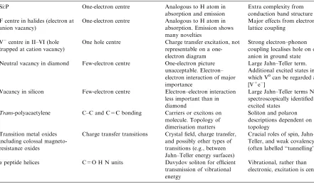
5. Varieties of excited states
evolve when, during cooling, it reaches states close to the cross-over, where there will be strong mixing of vibronic states associated with ground and excited electronic states. Near the cross-over, there will be a branching probability between evolution to vibrationally excited electronic ground states and to vibrationally excited electronic excited states. Much of this behaviour has been mapped, and can be understood in simple terms. The descriptions go beyond the misleading ‘‘sliding down energy surfaces’’ pictures once held. Clearly, issues of coherence emerge: is the relaxation process coherent in some sense? Is this simply classical vibrational coherence, or can we have some quantum coherence as well? (Table 1).
These issues are important whenever excitation modifies materials. Much is known of how self-trapped excitons localise energy, and create neutral halogen vacancy-interstitial pairs in alkali halides. This proves to be just one facet of a wide range of consequences of electronic excitation. For halides, band gaps are often larger than defect formation
energies. In semiconductors (with the possible exception of nitrides), there is even less energy available after band gap excitation, and typical excitation effects are defect metastability and recombination-enhanced diffusion. Enhanced dif-fusion can involve motion in an electronic excited state for which the energy surface is different (local excitation, as for F centres), motion through alternate capture of electrons and holes (Bour-goin–Corbett) and motion through enhanced vibrational motion (local heating). In non-equili-brium situations (during implantation, or rapid thermal anneals) control to ensure only the right species move is more likely to be achieved if appropriate excitation complements simple ther-mal anneals. The excitation of oxides leads not to new point defects, but to dislocation climb (and hence electrical breakdown), or to charge transfer. The excited states of amorphous silicas are an exception, with especial technological relevance. Optical fibres, gratings are written optically (some-times in the presence of an electrical field). The
Table 1
Spectroscopy and the nature of excited states[12,13]
Si:P One-electron centre Analogous to H atom in absorption and emission
Extra complexity from conduction band structure F centre in halides (electron at
anion vacancy)
One-electron centre Analogous to H atom in absorption. Emission shows many novelties
Major effects from electron– lattice coupling
Vcentre in II–VI (hole trapped at cation vacancy)
One hole centre Charge transfer excitation, not representable on a one-electron diagram
Strong electron–phonon coupling localises hole on one anion in ground state Neutral vacancy in diamond Few-electron centre One-electron picture
unacceptable. Electron– electron interaction of major importance
Large Jahn–Teller term. Additional excited states in which V0can be regarded as [V+e]
Vacancy in silicon Few-electron centre Electron–electron interaction less important than in diamond
Large Jahn–Teller terms No spectroscopically identified excited states
Trans-polyacaetylene C–C and C=C bonding Carriers or excitons on molecule. Topology of dimerisation matters
Soliton and polaron descriptions dependent on topology
Transition metal oxides including colossal magneto-resistance oxides
Charge transfer transitions Crystal field, charge transfer, and possibly other types of transitions (e.g., between Jahn–Teller energy surfaces)
Crucial roles of spin, Jahn– Teller, and weak covalency (often labelled ‘‘tunnelling’’)
apeptide helices C=O H N units Davydov soliton for efficient transmission of vibrational energy
compaction (undesirable change of density) of vitreous silica is a limit on its use in optical lithography. Certain of the breakdown processes of the amorphous silicon oxide gate dielectric involve excited states. Some, at least, of these processes can be ‘‘tamed’’, and the combination of selective excitation on the nanometer scale is potentially very powerful.
6. Quantum dots and dynamic relaxation
For many in the semiconductor community, a typical quantum dot is self-organised, with per-haps 10,000 atoms, showing a Coulomb blockade (more than energy kT at room temperature is needed to add a second carrier). For the photonics community, a dot has so few atoms as to show a blue shift in optical absorption or luminescence; it would contain perhaps 100–500 atoms. Both dots are, of course, much smaller than a grain of dust (typically 1016 atoms). When there are only 200 atoms, normal ideas of what is important can be changed. First is the ‘‘Nþ1’’ problem: a dot of 200 atoms (say Cd100Se100) is likely to have
significantly different properties from a dot of 201 or 202 atoms. This is especially true for an ionic dot, since there will be very large electric fields associated with the extra ions. Alloy fluctuations will rule out conventional band-gap engineering, but chemical impurities will usually be wholly unimportant. The Nþ1 problem implies that any ensemble of dots (which will have a distribution of diameters of few percent) is actually extremely inhomogeneous. Secondly, giv-ing the dot an eV or so of energy means a large temperature rise, unless heat loss is easy; such energy dissipation can be hard. Thirdly, changes in electronic state will cause large fractional changes in dot volume and lattice parameter (and even in thermal equilibrium, the root mean square volume fluctuations are a few percent). This can have surprising effects. Suppose one wished to use a 200-atom dot as a means of rapid switching in photonics. One might excite the dot with a laser; in its excited state, the refractive index would be different, causing switching; one would then want to de-excite using the same laser, giving a very
rapid process overall, perhaps taking a few picoseconds. The problem is that the dot also changes its volume in the excited state because the excitation changes interatomic forces. This is the same reason that defect formation, or exciton formation, changes the volume of a bulk crystal. In fact, the volume change is largely independent of dot size. Thestrain, however, is much larger for a smaller dot, as is the energy shift through the deformation potential. Reasonable estimates sug-gest that the characteristic energy for de-excitation will shift out of the laser line width in a time similar to the planned switching time. There will (apparently) be a loss of coherence[14]. Such a loss of coherence is observed [15]. Here we have a system which seems very simple, and which reminds us of the care we need to tame it.
parameter for non-radiative transitions is the ratio of the time to lose one phonon of energy to the period of vibration. For many dot systems, the presence of hot luminescence shows that cooling is slow, with this ratio large. Yet other work [20]
suggests fast electron de-excitation involving surface species. There is a wealth of semicond-uctor surface processes caused by electronic excitation[21].
Optical de-excitation can be radiative (stimu-lated or spontaneous) or radiative. A non-radiative transition might put 3 eV into a dot of 100 atoms, which corresponds to a temperature rise of nearly 350. It is not surprising that there
are observations of dots behaving in unusual ways, with changes in structure, or ceasing to luminesce for a period. Suffice it to say that there are several possible mechanisms to be considered when one wants to assess dots for demanding applications. For changes in structure (loss or change of diffraction peaks [22]), explanations include rota-tion of the dot, photochemical effects involving substrate species (e.g., H2O, or C oxidation),
melting or quasi-melting [23]or a change of ionic configuration following an internal charge trans-fer. The loss of luminescence [24] is usually attributed to a change of charge state, e.g., due to an Auger process following excitation of a second exciton, or to some ‘‘dark’’ state. The ‘‘dark’’ state might have a long lifetime because of a spatial selection rule (at least for a high-symmetry dot), because of e–h separation through an internal field, or because of a spin-flip into a triplet state. Current theories are not especially helpful in determining mechanisms: density func-tional theories fail to localise charge even in cases for which localisation is certain, whereas Hartree– Fock theories localise in cases where it is should not be seen [16].
Dynamics involves several distinct processes. If a system stays in the same electronic state, vibrational energy will evolve from some coherent motion to heat, an incoherent motion. The cooling transitions can include relaxation towards a self-trapped state. Electron–lattice coupling also causes non-radiative transitions with change of electronic state. In all these cases, the shortest characteristic times will be similar to lattice vibrational periods.
Here coherentmeans classical coherence: a corre-lated motion of atoms which can be described on a standard configuration coordinate diagram. Motion in the reaction coordinate becomes less coherent, partly by dephasing as different normal modes get out of step due to their spread of frequencies. It is classical vibrational coherence which has been exploited in molecular systems to select a particular excited state dynamically. Vibrational coherence is evident in studies of low-frequency motions of ions near the interface between II and VI quantum dots and an a-SiO2
matrix. It is also a component in the so-called Davidov soliton which transfers energy along the
a-helix of a protein.
7. Quantum information technology
Quantum coherence in excited states is both more subtle and harder to achieve, but a possible route to quantum information technologies [2]. Quantum information technology (QIT) includes various aspects of encryption, decryption, and many possibilities beyond quantum computing. The basic ideas are these. Whereas classical information processing (CIT) use bits (0 or 1), QIT uses qubits which are linear combinations
aj0>þbj1> : This has three bonuses: (i) much information can be encoded in theaandb; (ii) the Schrodinger equation is linear, so parallel manip-. ulation is possible; (iii) the state ‘‘knows’’ when it is observed, since it will become either |0> or |1>, so information security measures are possible. In CIT, the bits are manipulated by gates, and a small number of linked universal gates enables all the wizardry and frustrations we know so well. In QIT, there are again universal gates, but of just two types. So-calledA-gatesmanipulate individual qubits, controlling the a and the b. So-called
quantum information is lost, both from an individual qubit and in the coherent dance of two qubits. Quantum decoherence corresponds closely to classical dissipation. There is an inter-esting battle between switching speed and deco-herence, governed by the fluctuation-dissipation theorem[25].
An important aim in QIT is switching on and off the interactions between qubits, so as to cause entanglement when the interaction is on, and yet store quantum information when the interaction is off. The contrast is important. At UCL, our approach[5]exploits excited states. Imagine a pair of spins which have negligible interaction. Once entangled, they would store quantum information. Imagine next an excited state in which the spins do interact. Then the excitation can be used to control the entanglement, using processes which do not interfere with subsequent quantum information storage. Possible processes might be the simple excitation of a donor pair [D+D+ee] -[D+D+ee], or a charge transfer from a control atom [D+D+ee]+[C+e]-[D+D+eee]+[C+], or a number of other options. The main requirement is that the ground state donors have spin, and that
there is an accessible molecular excited state to enable coupling.
Of course, we would have to be sure that the excitation does not couple in quantum informa-tion or decoherence from some other source. This can be arranged with sensible parameters[5,26]. Of course, we should have to be sure we only couple through excitation those qubits that we wish to entangle. But there are some very clear opportu-nities. First, the characteristic energies are those of the excitation, and can be large compared with thermal energies, even at room temperature. The key idea is to use as qubits the electron spins of deep impurities D which are not ionised at the working temperature. Secondly, a non-uniform distribution of donors is a virtue. The impurities D are distributed randomly, at a spacing which is typically larger than that at which they interact significantly. What is especially important is that one can exploit the randomness of the D distribu-tion, since this will lead to variations of excitation energy from one D pair to another. Given that the lengths characteristic of the molecular-type excited state are perhaps 10 nm, much less than the likely excitation wavelengths (perhaps 1000 nm), one
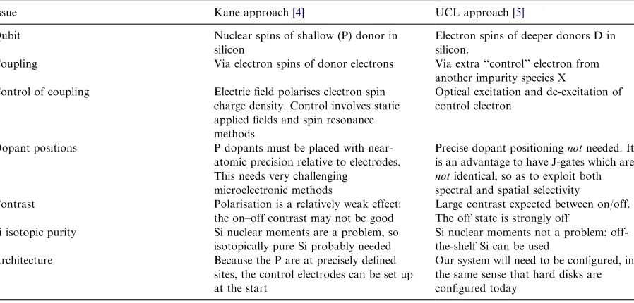
Table 2
Kane and UCL J-gates: a comparison
Issue Kane approach[4] UCL approach[5]
Qubit Nuclear spins of shallow (P) donor in silicon
Electron spins of deeper donors D in silicon.
Coupling Via electron spins of donor electrons Via extra ‘‘control’’ electron from another impurity species X Control of coupling Electric field polarises electron spin
charge density. Control involves static applied fields and spin resonance methods
Optical excitation and de-excitation of control electron
Dopant positions P dopants must be placed with near-atomic precision relative to electrodes. This needs very challenging
microelectronic methods
Precise dopant positioningnotneeded. It is an advantage to have J-gates which are
notidentical, so as to exploit both spectral and spatial selectivity Contrast Polarisation is a relatively weak effect:
the on–off contrast may not be good
Large contrast expected between on/off. The off state is strongly off
Si isotopic purity Si nuclear moments are a problem, so isotopically pure Si probably needed
Si nuclear moments not a problem; off-the-shelf Si can be used
Architecture Because the P are at precisely defined sites, the control electrodes can be set up at the start
cannot pick out a single qubit pair merely by using high-resolution optics. Selecting a particular D-pair J-gate involves both spatial and spectral selectivity, i.e., using photons of the right wave-length for that pair. Getting this to work, of course, involves achieving quite a few interdepen-dent goals. A crucial central factor is what I call ‘‘excited state engineering’’, in that one needs to optimise interactions and to ensure excited states couple two spins, not many spins.
Kane’s original ideas have been seminal. He was the first to suggest [4] a silicon-based quantum processor, and his ideas have led many others to consider this route. It may perhaps be helpful to compare the Kane approach with ours (Table 2).
If based on silicon, our approach may make quantum information processing possible at room temperature in devices which, because they work with random dopant placings, might be made largely by off-the-shelf methods. The shelf in question is, of course, not the average shelf, but one which has the current best tools available. So we have an approach, based on systems and methods not far from current practice, which could make possible quantum information proces-sing even at room temperature.
8. Conclusion
The excitation of semiconductor defects opens a rich variety of new phenomena. There are new approaches to defect processes and processing. There are new ways to work with the smaller length scales of nanoscience, whether through a Coulomb blockade, optical confinement, or ex-cited state engineering. There is even an opportu-nity to exploit the subtle world of quantum effects. Whether these developments constitute a new ‘‘programme for the future’’ [27] is still to be decided.
Acknowledgements
This work was supported in part by EPSRC through projects GR/S23506 and GR/M67865EP69.
I am indebted to my colleagues for their enthu-siasm and insights.
References
[1] N. Itoh, A.M. Stoneham, Materials Modification by Electronic Excitation, Cambridge University Press, Cambridge, 2001.
[2] C.P. Williams, S.H. Clearwater, Ultimate Zero and One: Computing at the Quantum Frontier, Copernicus, Springer, New York, 2000;
P.T. Greenland, Philos. Trans. Roy. Soc. A 361 (2003) 379. [3] E. Klarreich, Nature 413 (2001) 450;
M. Bruchez, M. Moronne, P. Gin, S. Weiss, P. Alivasatos, Science 281 (1998) 2013;
W. Chan, S. Nie, Science 281 (2001) 2016. [4] B.E. Kane, Nature 393 (1999) 305;
R.G. Clark, et al., Philos. Trans. Roy. Soc. A 361 (2003) 1451.
[5] A.M. Stoneham, A.J. Fisher, P.T. Greenland, J.Phys.: Condens. Matter 15 (2003) L447;
A.M. Stoneham, A.J. Fisher, P.T. Greenland, British Patent Application No 02050011.0 A Gate for Quantum Information Processing, filed 4 March 2002.
[6] A.M. Stoneham, Mater. Sci. Eng. C 23 (2003) 235–241. [7] A.M. Stoneham, J.H. Harding, Nat. Mater. 2 (2003) 77. [8] A.M. Stoneham, M.M.D. Ramos, R. Ribeiro, Appl. Phys.
A 69 (1999) S81;
J.T. Dickinson, S.C. Langford, J.J. Shin, D.L. Doering, Phys. Rev. Lett. 73 (1994) 2630;
C. Bandis, S.C. Langford, J.T. Dickinson, Appl. Phys. Lett. 76 (2000) 421.
[9] A.M. Stoneham, Semicond. Sci. Technol. 17 (2002) L15. [10] A.M. Stoneham, Rev. Solid State Sci. 4 (213) (1990) 161. [11] A.M. Stoneham, Radiat. Eff. 142 (1996) 191.
[12] A.M. Stoneham, Radiat. Eff. Def. Solids 154 (2001) 179. [13] F. Bridges, et al., J. Phys.: Condens. Matter 2 (1990) 2875;
A.M. Stoneham, N. Itoh, Appl. Surf. Sci. 168 (2000) 186; W. Hayes, A.M. Stoneham, Defects and Defect Processes in Non-Metallic Solids, Wiley, New York, 1985; W. Beall Fowler, Physics of Color Centers, Academic Press, New York, 1968;
A.M. Stoneham, Theory of Defects in Solids, Oxford University Press, Oxford, 1996.
[14] A.M. Stoneham, B. McKinnon, J. Phys.: Condens. Matter 10 (1998) 7665.
[15] D.M. Mittelman, R.W. Schoenlein, J.J. Shiang, V.L. Colvin, A.P. Alivasatos, C.V. Shank, Phys. Rev. B 49 (1994) 14435.
[16] J.L. Gavartin, A.M. Stoneham, Philos. Trans. Roy. Soc. A 361 (2003) 275.
[17] A. Hagfeld, M. Gratzel, Acc. Chem. Res. 33 (2000) 269.. [18] A.M. Stoneham, Solid State Commun. 3 (1965) 71. [19] U. Woggon, Optical Properties of Semiconductor
[20] Q. Darugar, C. landes, S. Link, A. Schill, M.A. El-Sayed, Chem. Phys. Lett. 373 (2003) 284.
[21] N. Itoh, A.M. Stoneham, J. Phys.: Condens. Matter 13 (2001) R489.
[22] P.A. Buffat, Philos. Trans. Roy. Soc. A 361 (2003) 291. [23] R.R. Hudgins, et al., Phys. Rev. Lett. 78 (1997) 4213. [24] A.V. Baranov, S. Yamauchi, Y. Masumoto, Phys. Rev.
B 56 (1997) 10332;
A.V. Fedorov, A.V. Baranov, Sov. Phys. JETP 83 (1996) 610;
T. Itoh, M. Nishijima, A.I. Ekimov, C. Gourdon, A.L. Efros, M. Rosen, Phys. Rev. Lett. 74 (1995) 1645; K. Inoue, A. Yamanaka, K. Toba, A.V. Baranov, A.A. Onushchenko, A.V. Fedorov, Phys. Rev. B 54 (1996) 8321. [25] A.J. Fisher, Philos. Trans. Roy. Soc. A 361 (2003)
1441.