Early Propagation and Imbalanced Routing,
How to Diminish in FPGAs
Amir Moradi1 and Vincent Immler2?
1 Horst G¨ortz Institute for IT Security, Ruhr University Bochum, Germany 2
Fraunhofer Research Institution for Applied and Integrated Security (AISEC), Munich, Germany
[email protected], [email protected]
Abstract. This work deals with DPA-resistant logic styles, i.e., cell-level countermeasures against power analysis attacks that are known as a serious threat to cryptographic devices. Early propagation and imbal-anced routings are amongst the well-known issues of such countermea-sures, that – if not considered during the design process – can cause the underlying cryptographic device to be vulnerable to certain attacks. Although most of the DPA-resistant logic styles target an ASIC design process, there are a few attempts to apply them in an FPGA platform. This is due to the missing freedom in FPGA design tools required to deal with the aforementioned problems. Our contribution in this work is to provide solutions for both early propagation and imbalanced routings considering a modern Xilinx FPGA as the target platform. Foremost, based on the WDDL concept we design a new FPGA-based logic style without early propagation in both precharge and evaluation phases. Ad-ditionally, with respect to the limited routing resources within an FPGA we develop a customized router to find the best appropriate dual-rail routes for a given dual-rail circuit. Based on practical experiments on a Virtex-5 FPGA our evaluations verify the efficiency of each of our pro-posed approaches. They significantly improve the resistance of the design compared to cases not benefiting from our schemes.
1
Introduction
Counteracting state-of-the-art power analysis attacks (so called DPA [13]) is a must for cryptographic devices which may fall into the hands of malicious users, who can control over the device in a hostile environment. Up to now several DPA countermeasures at different levels of abstraction have been proposed. Many try to provide resistance by manipulating the underlying cryptographic algorithm in order to randomize its intermediate values, i.e., masking at the algorithmic level, e.g., [24, 25]. Some introduce noise, e.g., [7, 17] or randomize either the program flow or the order of the operations, i.e., shuffling, e.g., [10, 17]. A couple
?
of other schemes try to solve the problem from scratch, i.e., avoiding the de-pendency of the power consumption of the circuit to the processed data. These countermeasures at the cell level, called DPA-resistant logic styles, aim at equal-izing the power consumption of a cryptographic device regardless of any input, intermediate, or output value.
After a proper evaluation [30] it was discovered that most of the proposed logic styles, such as WDDL [32] and MDPL [27], suffer from the early propagation effect. This phenomena, also called data-dependent time-of-evaluation, refers to the cases where a gate fires (evaluates) its output at different time instances depending on the value of its input. It becomes more problematic when several of such gates are cascaded to realize a combinatorial circuit. So, it causes the power consumption pattern of the circuit to have a clear dependency to its input value.
Moreover, most of the known logic styles face a common difficulty, i.e., routing imbalances. Equal power consumption, which is expected to be achieved by Dual-Rail Precharge (DRP) logic, needs a proper balance between the capacitances of each dual-rail signal. Otherwise, transitions of TRUE and FALSE lines of a dual-rail signal require different amounts of energy, which can be explored by a DPA attack. Therefore, some place-and-route methods such as [6, 33] have been proposed to diminish the load imbalances of complementary signals in an ASIC design process. Although iMDPL [26], which solves the early propagation effect of MDPL, was designed to relax the necessity of balanced routings, still has exploitable leakages due to imbalanced routing of the dual-rail mask signal [20].
State-of-the-Art Even though most of the proposed logic styles target an ASIC platform, at the early stage of their development some have been evaluated using FPGAs. Since the FPGA design tools miss the flexibility required for balanced routing, most of the efforts in this direction led to duplication schemes. They follow the idea of dual-rail concept without precharging the signals. This indeed leads to making a dual copy of a fully placed-and-routed circuit which – in theory – should consume the complement amount of energy that the original counterpart does. However, the problem arising by this scheme is due to non-dual glitches happening in original and non-dual part of the circuit, that causes the design to be vulnerable to the state-of-the-art attacks.
In this direction we can refer to [11], where – in addition to the dual of the circuit – precharge registers are inserted to the design. As the authors also showed, their design can be broken because of glitches. In another work [8] a specific configuration for FPGA Look-Up-Tables (LUT) is used to make the delay of the gates constant. Two global signals connected to all LUTs are also used to handle the precharge and evaluation of the gates. After developing the circuit by this configuration, the dual part of the circuit is inserted to the design. Unfortunately their design still has glitches when the combinatorial circuit has two or more logic depth.
which make use of the duplication on the circuits built by FPGA Block RAMs (BRAM). For example, the authors of [34] introduced a precharge signal for each BRAM address in order to provide precharge and evaluation phases in this con-text. By certain inappropriate assumptions, e.g., ignoring the leakage associated to glitches occurring at the LUTs’ output as long as they do not leave the slice, they developed a design methodology.
In the work of [28] the authors tried to realize WDDL on an Altera Stratix-II FPGA. They used DES as the target algorithm and have examined two different place-and-route (PAR) strategies as 1) theTRUEandFALSE signals of each gate are placed and routed as close as possible, and 2) allTRUEsignals are placed close together (the same for allFALSEsignals). The drawbacks of their work are 1) no attempt to avoid early propagation, and 2) no control over the delay between the rails of dual-rail signals.
In another work [15] a triple-rail logic has been designed for a Xilinx Spartan-3 FPGA. In order to avoid early propagation in both precharge and evaluation phases they utilized a generalized form of Muller C-element (the main element of asynchronous logic designs [22]). Although the goal of preventing early prop-agation is fulfilled, the number of toggles happening at internal signals is not balanced, i.e., they are different depending on the gate inputs’ value. It is be-cause 6 LUTs are used to build a triple-rail gate, and the toggles of output of these 6 LUTs are not balanced for all input cases. Therefore, it most likely leads to different power consumption patterns detectable by a DPA attack.
Other works e.g., BCDL [23] employed a global precharge signal, which must be connected to all gates. The gates do not evaluate their output till the global precharge goes e.g., LOW thereby preventing early propagation in both phases. But at the start of the precharge phase all gates simultaneously precharge their output leading to a much higher power consumption peak compared to the eval-uation phase. Based on an Altera Stratix-II FPGA each BCDL gate is realized by two 5-input LUTs, but they have not taken care about the routing of dual-rail signals.
In a follow-up work [3] the global precharge of BCDL is removed and following the WDDL concept each gate is actualized by two 4-input LUTs. The style, which is called DPL noEE, prevents the early propagation in the evaluation phase, but nothing is considered to deal with the start of the precharge phase. Similar to the case of BCDL, a Stratix-II FPGA has been used for practical evaluation of an AES encryption module under DPL noEE scheme. According to the claims of the authors, the leakage could be reduced to half while no restrictions have been put into the placement and routing processes.
In the second part of this article we aim at designing a variant of WDDL for FPGA platforms without early propagation in both phases. With the help of the asynchronous design concept we achieve an architecture which follows the WDDL definitions, but its time-of-evaluation as well as its time-of-precharge is independent of the processed values. More importantly it propagates the evalu-ation wave (resp. the precharge wave) only when all inputs are evaluated (resp. precharged).
However, the imbalanced routings caused by uncontrolled FPGA design tools (placer and router) makes the power consumption of the circuit to be still re-lated to its input value. Therefore, the next contribution of this article deals with balanced dual-rail routing in FPGAs. By means of a sophisticated routing algorithm as well as information we extract about the route delays, we are able to route the dual-rail signals with minimum imbalances. As a target design and platform we selected an AES S-box to be realized on a Xilinx Virtex-5 FPGA. Our experimental results show that both (more) balanced routings and avoiding early propagation significantly reduce the amount of leakage extractable by a power analysis attack.
2
WDDL and Early Propagation
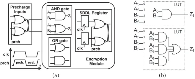
Wave Dynamic Differential Logic (WDDL) was developed to avoid the necessity of a full-custom design tool. Similar to other precharge logic styles every gate operates in two phases, i.e., precharge and evaluation, which are controlled by the clock signal. However, as shown by Fig. 1(a) the signals are converted to dual-rail precharge form prior to the WDDL circuit, and the clock signal is not routed to the WDDL logic cells. Figure 1(a) shows the concept and the design of a WDDL AND/NAND gate. These gates can straightforwardly be actualized by FPGA LUTs, but the concept which is followed by DPL noEE [3] is shown in Fig. 1(b). The idea is to prevent the evaluation as long as the inputs are not complete3.
In order to deal with early propagation issue we first assume that though the delay of different dual rails are not the same, the delay of TRUE and FALSE
signals of each dual rail are the same. In other words,
Delay(At) = Delay(Af) > Delay(Bt) = Delay(Bf).
Figure 2 depicts the timing diagram of three different cases of the inputs for both WDDL and DPL noEE AND/NAND gates. By comparing cases 1 and 3 (∆te1 vs. ∆te3) we can conclude that the start of the evaluation phase of the WDDL gate depends on its input values. This issue, which is addressed in [30], is known as data-dependent time-of-evaluation. Examining cases 1 and 2 (∆tp1 vs.∆tp2) also shows the dependency of the start of the precharge phase to the gate input, which is referred as data-dependent time-of-precharge.
3
(a) Zf At Af Bt Bf 0 1 2 3 LUT Af Bf Af Bt At Bf Zt At Af Bt Bf 0 1 2 3 LUT At Bt (b)
Fig. 1.(a) WDDL concept (taken from [32]), (b) DPL noEE AND/NAND gate
0
1
clk At Af Bt Bf Zt Zf eval.Δte1 t
prch.
Δtp1
0
0
clk At Af Bt Bf Zt Zf eval.Δte2 t
prch.
Δtp2
1
1
clk At Af Bt Bf Zt Zf eval.Δte3 t prch.
Δtp3
(noEE)Zf (noEE)Zf (noEE)Zt
case 1 case 2 case 3
Fig. 2. Timing diagram of three input cases, WDDL and DPL noEE AND/NAND gates
The situation for DPL noEE is different as its time-of-evaluation is data in-dependent. It also instantly goes to the precharge phase once one of its inputs goes to precharge. Although its time-of-precharge does not depend on its input value, it fits to the definition ofearly propagation in precharge phase. We should refer to [26], where it is stated as “According to our analysis, DRSL does not completely avoid an early propagation effect in the precharge phase”. From this perspective DPL noEE and DRSL [5] have the same specification. Both have data-independent time-of-evaluation and time-of-precharge, and both do not avoid early propagation in the precharge phase. On the contrary, the precharge phase of each iMDPL [26] gate starts when all its inputs are in precharge. Here the question is how critical it is to not avoid early propagation in precharge phase while it is data independent?
To answer this question we should highlight two points:
At Af Bt Bf
Zt
At Bt St
Rt At
Af Bt Bf
0 1 2 3
4
LUT
S-R Latch
At Af Bt Bf
Zf
Af Bf
Sf Rf At
Af Bt Bf
0 1 2 3
4
LUT
S-R Latch Af
Bt At Bf
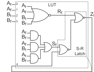
Fig. 3.AWDDL AND/NAND gate4
power consumption peak in the precharge phase is expected to be higher. The same is observed when a global precharge signal is used as in SABL [31]. – All the statements given above about the data independence of time-of-evaluation as well as of time-of-precharge are valid as long as the first as-sumption Delay(At) = Delay(Af) (resp. Delay(Bt) = Delay(Bf)) holds. If the routings are imbalanced and this assumption is not valid, both time-of-evaluation and time-of-precharge would be data dependent.
Therefore, in this setting we expect that the leakage in the precharge phase is more easily detectable compared to that in the evaluation phase since slight rout-ing imbalances still would exist in practice. We deal with this issue in Section 4 when we demonstrate the corresponding practical results.
2.1 Avoiding Early Propagation in both Phases
Our goal here is to develop a design similar to DPL noEE but without early propagation in the precharge phase. So, we consider an asynchronous design for each WDDL gate. Following standard asynchronous design schemes one can make the flow table for the desired gate behavior, and realize it using e.g., S-R approach, where S-R latches are utilized. Figure 3 shows an exemplary design of our desired WDDL AND gate, which we call Asynchronous WDDL (AWDDL). Note that this design is only suitable for the FPGA platforms to realize the gate outputs by LUTs. It cannot be considered as an ASIC solution due to the unbalanced number of toggles happening on the internal signals. Since we use a modern Xilinx FPGA as the target platform, every gate is realized by two hard-coded LUT6 instances, i.e., to provideZtandZf. Furthermore, every LUT output should be routed to its input, i.e., an external loop around every LUT
4
is essential. Since the 6-input LUTs are the currently biggest LUT available in FPGA architectures, unfortunately our proposed scheme cannot be extended to consider one more dual-rail mask input signal to realize a kind of iMDPL cell [26].
With respect to the asynchronous design concept and the S-R latches our design of AWDDL guarantees no early propagation in both precharge and eval-uation phases. Due to the lack of space we omit presenting the figures for other AWDDL gates. However, the formulas for the set and reset signals (S,R) of the conceptual S-R latch of 2-input gates are listed below. Similar to WDDL, the in-verted gate is realized by swapping the dual-rail output signals. Below, + stands for the logical OR operation.
all gates : Rt=Rf =At+Af+Bt+Bf
AND :
St=AtBt
Sf =AfBf+AfBt+AtBf
OR :
St=AtBt+AtBf+AfBt Sf =AfBf
XOR :
St=AtBf +AfBt Sf =AtBt+AfBf
We should emphasize that we are aware of the problem of single-rail WDDL register cells mentioned in [19]. Our contribution focuses on the combinatorial part of the logic style, and as stated in [19], the master-slave register cells must be used to prevent the leakage of the registers.
3
Dual-Rail Routing
The problem of dual-rail routing is a challenge to perfectly balance the capac-itance of both rails of a signal. Otherwise, transitions on these signals need a different amount of energy, which may make it possible to distinguish on which rail the transition happens. On the other hand, the capacitive imbalance causes the delay of the rails to be different. Then, the arrival time of a dual-rail input signal of a gate depends on its value. Since a gate without early propagation in both phases, e.g., our AWDDL, fires (resp. precharge) the output when all input signals arrived (resp. precharged), the time of evaluation (resp. precharge) of the gate will still depend on its inputs’ value. This propagates through the whole combinatorial circuit, and makes the power consumption patterns different depending on the circuit input value.
.LOG
.SCR
Xilinx
map bitgenXilinx
Xilinx
FPGA Editor
(fpga_edline)
Xilinx
xdl
modified BYU RapidSmith Tools + SAT solver
Xilinx
xdl
.SCR .LOG
.NCD .NCD
.XDL .SCR .LOG .XDL
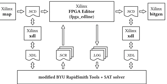
Fig. 4. Illustration of the custom workflow to process designs containing dual-rails requiring balanced routing
every gate requires to have both TRUE and FALSErails of all input signals. For the same reason we cannot make use of the approach presented in [9] because their scheme is also based on complete separation of TRUE andFALSEnetworks. Therefore, we need to develop a mechanism capable of routing dual-rail signals as balanced as possible. While it is unlikely to achieve a perfectly balanced routing due to the given structure of the FPGA, it is likely to reduce the leakage compared to the default routing of the FPGA standard tools. We tried to achieve this by developing a customized router which is presented hereafter.
3.1 Customized Router
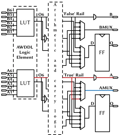
As stated before, our target is a Xilinx Virtex-5 FPGA; therefore, we could make use of the RapidSmith library [14]. In order to route balanced dual-rails we implemented a customized local router. It utilizes the Xilinx Design Language (XDL) and is based on a custom workflow as depicted in Fig. 4. Up to the end of mapping, the design is processed by the default Xilinx ISE tools. Note that for the case of Virtex-5mapperforms the placement as well. The only modifications we made up to this step are i) to put all elements requiring balanced routing into a closed group which is area constrained, ii) to keep the input PIN positions of the LUTs realizing the AWDDL gates locked, and iii) to put LUTs of each AWDDL gate into the same slice using the LUTs (A, B) or (C, D) for (Zt,Zf) respectively.
AWDDL Logic Element A r i t h m e t i c a n d c a r r y l o g i c LUT FF A1 A2 A3 A4 A5 A6 O6 A AMUX LUT B BMUX D B1 B2 B3 B4 B5 B6 O6 FF D Q Q 'False' Rail 'True' Rail
(a) Each pair of LUTs hold a single AWDDL logic element. Hence, a maximum of two AWDDL gates per slice is possible.
A AMUX
BMUX B
(b) A simplified represen-tation of a switch box. Blue and red dots repre-sent PIPs that may be used as exit node.
Fig. 5.Basic idea how to create multiple routing candidates
routing itself for each of these candidates uses a maze router with a priority queuing, favoring those nodes with the least Manhattan distance. This process is executed for both connections of a dual-rail to finally make a set of possible routings for each of the dual-rail connections.
Since extracting the capacitance of each route is not feasible, we had to consider other metrics to give priorities to the different routings. They include:
– the signal delays, extracted using the command line toolfpga edline(due to the phenomena expressed above),
– the number of switch boxes the signal passes (due to their significant role in amount of dynamic energy consumption),
– the number of Programmable Interconnect Points (PIP), i.e., internal con-nections of the switch boxes, and
– the type of the wire, e.g.,long,pent, anddouble.
open design ncdFileName.ncf pcfFileName.pcf setattr main edit-mode Read-Only
setattr main auto_load_delays true select netName
delay exit exit5
The result of running this script is a log file (.log) that contains the delay information of every route within that net. It is therefore required to parse the log files and extract the only valid delay for the route made (see Fig. 4). Note that for each single route the corresponding NCD file must be generated. Then, the above script and process should be run to extract the associated delay.
Here we make the restrictions. Based on the extracted information (as ex-plained above) we restrict the dual-rail routes based on a threshold for delay of each route, for the difference between delay of the rails, for the number of switch boxes each route passes, for the number of PIPs, and etc. As the last step, as given below, the output is converted into a Boolean satisfiability (SAT) prob-lem to select a conflict-free routing. If the probprob-lem is satisfiable, the conflict-free setting is put together and written to a new XDL file. All the previously routed nets are then locked, while the remaining unrouted nets are auto-routed using
fpga edline.
3.2 Representing Routing as SAT
Letndenote the number of dual-rail connections that the router should make. We first make a collection S={S1, S2, . . . , Sn}, whereSi∈{1,...,n} represents a
set of possible routing candidates{si1, si2, . . . , sini}for the dual-rail connectioni.
Accordingly we define Boolean variablesxijindicating whether the dual-route si
j is selected. Clearly, one must select exactly one candidate sij from each set Si to achieve a complete routing. This requirement can be encoded using the following formula [12]:
AtLeastOne(Si) = n _
j=1 xij,
AtMostOne(Si) = n−1
^
j=1 n ^
k=j+1
(¬xij∨ ¬xik),
ExactlyOne(Si) = AtLeastOne(Si)∧AtMostOne(Si).
Therefore, ExactlyOne(Si) =TRUE for ∀i∈ {1, . . . , n} are added as clauses to the SAT.
Another issue is related to the loop which must be made at every LUT. As stated in Section 2.1, the output of the LUT must be presented as one of
5
its inputs to realize the internal S-R latch. For simplicity and consistency we tried to make the same loop at every LUT which is used as AWDDL gate. To achieve this we define collection S? = {S?1, S?2, . . . , S?l}, where l denotes the number of possible dual-rail loop routings, and S?i∈{1,...,l} a set of the same
dual-rail loop routing for all AWDDL gates of the design, i.e., {s?i
1, . . . , s?im}, wheremstands for the number of AWDDL gates in the design. Therefore, only one of these sets amongst collectionS?must be selected. Accordingly we define
Boolean variablesx?i
j due to the selection of the routings?ij . Moreover, a set of l commander-variables C = {c1, . . . , cl} are defined indicating the selection of S?1, . . . , S?l.
In order to consider the commander-variables into the SAT, one needs to include ExactlyOne(C) =TRUEto make sure that only one loop set is selected. Moreover, the following formula must be also considered to prevent a selection of a mixture of different loop sets:
AllFalse(S?i) =ci∨ m ^
j=1
¬x?ij AllTrue(S?i) =¬ci∨ m ^
j=1 x?ij .
Therefore, AllFalse(S?i) =TRUEand AllTrue(S?i) =TRUEfor∀i∈ {1, . . . , l}are added to the SAT.
We should emphasize that two slices are connected to the same switch box, and we use either (A, B) or (C, D) LUTs to realize each AWDDL gate. Since the loop routing possibilities of these cases are different, we have to consider four dif-ferent S? collections (and four different commander-variable setC respectively)
to cover all these cases.
However, the above illustrated expressions do not reflect possible routing conflicts yet. The conflicts must also be encoded by doing a pairwise comparison of all possible routing candidates, and the corresponding clauses must be added to the SAT. Suppose thatxi
jandxi
0
j0 are corresponding Boolean variables of two
conflicting routings si j and s
i06=i
j0 . So,¬xij∨ ¬xi 0
j0 =TRUE must be added to the
SAT. This should be done for all possible pairwise conflicting routings (extracted by means of RapidSmith) including those which can be between collections S
and S?. This encoding can be realized inO(n2). It should be noted that if the
SAT solver fails to find a conflict-free solution, the restrictions – explained at the end of Section 3.1 – to make collectionsSandS? should be relaxed and the
process should be repeated.
The runtime of the whole process is determined by the slow file conversion (Xilinx ISE tools) from NCD to XDL and vice-versa. This step needs to be ex-ecuted for each delay extraction and though being massively parallelized using 16 cores (siblings), still takes around 6 hours for a design including m = 122 AWDDL gates and 8 additional LUTs for the single-to-dual rail conversion, where n= 606 dual-rail connections should be made. In contrast, SAT encod-ing typically requires about 20 minutes and solvencod-ing less than a minute usencod-ing
eni
Sbox WDDL/noEE/
AWDDL to
WDDL
Control Logic
prch eno
in out
(a) (b)
Fig. 6. (a) The exemplary design block diagram, (b) Superimposition of 256 mean traces of the WDDL design
4
Practical Investigations
In order to examine the effectiveness of our proposed schemes we made an exem-plary design which in addition to surrounding and control logics consists in an AES S-box. We have taken the area-optimized S-box by Canright [4], and man-ually instantiated all the logic by 2-input AWDDL gates (in sum 122). A block diagram of the design is shown by Fig. 6(a). The Virtex-5 FPGA (XC5VLX50) of the sichannel evaluation platform SASEBO-GII [2], on which our target de-sign is embedded, receives an input byte from the PC (via a controlling FPGA) and stores it into the input register by controllingeni signal. At a certain clock cycle, the control logic disablesprchsignal, and the “to WDDL” conversion unit (the same scheme shown in the left part of Fig. 1(a)) propagates the dual-rail input to the AWDDL AES S-box thereby initializing the evaluation phase. In the next half of the clock cycle the control logic enables prch signal and the precharge phase is started. In a common WDDL circuitenoshould be active at the start of the precharge phase in order to store the output of the combinato-rial circuit (here the AES S-box). However, since we aim at evaluating only the leakage associated to the combinatorial circuit, we must exclude the leakage of the output register (see [19]). Therefore, the control logic does not enable eno signal and the register does not store the S-box output6. During these two (eval-uation and precharge) phases the power consumption of the Virtex-5 FPGA is measured using a LeCroy WaveRunner HRO 66Zi oscilloscope at the sampling rate of 1GS/s while the design runs at a clock frequency of 3 MHz.
At the first step, we defined an area in the target FPGA for the placement of AWDDL gates, and as stated before we constrained the placer to assign two LUTs of the same slice to each AWDDL gate. At this stage we did not apply our customized router and used the default ISE routing tools. For the sake of similarity and fair comparison, we made also a WDDL and DPL noEE
com-6 In order to check the correct functionality of the circuit,en
o signal becomes active
0 50 100 150 200 250 300 350
0 50 100 150 200 250 >300
No.
of
o
ccurences
Delay Difference [ps]
our customized router ISE router
1
Fig. 7.Histogram of the delay difference of all dual-rail routes of AWDDL designs
patible version of the fully placed-and-routed AWDDL design. This has been done by editing the XDL file (of the AWDDL design) and only modifying the content of the LUTs7. So, the placement and routing of all these three designs are the same allowing for a fair comparison. As the fourth design we used our customized router in order to route the AWDDL design while its placement has not been altered.
In sum we evaluated four design profiles as:
1. WDDL AES S-box routed by ISE,
2. DPL noEE AES S-box, the same placement and routing as profile 1, 3. AWDDL AES S-box, the same placement and routing as profile 1,
4. AWDDL AES S-box, the same placement as profile 1, but routed by our customized router.
As listed in Section 3.1, we have considered many different criteria to make routing collectionsS andS?. The best result is achieved by considering a delay difference below 60 ps, the realization of identical feedback loops, and by consid-ering minimum number of switch boxes and PIPs in each route. It should also be mentioned that we used the same wire type for both rails of a signal and prohibited to use longwires.
In order to compare the result of our routing with that of ISE, we provided two histograms illustrating the difference between the delay of each dual-rail signal in the AWDDL S-box circuit. Although it is not possible to find dual-rail routes with zero delay difference for all 606 dual-rail connections, the histograms shown in Fig. 7 indicate the effectiveness of our approach. Nevertheless, it is worth to mention that the average and the worst delay difference in case of our router are 11.7 ps and 58 ps respectively. These numbers are incomparable to those obtained by the ISE router as 125 ps and 520 ps respectively.
To evaluate and fairly compare the side-channel leakage of our target designs we applied the information theoretic (IT) analysis of [29] as it has been used for
7 Although it is possible to realize each WDDL as well as DPL noEE gate by a 5-to-2
the same purpose e.g., in [16]. So, we collected 512,000 traces for each target design, i.e., 2000 traces for each S-box input value. By estimating the mean and variance of the traces for each S-box input we obtained 256 Gaussian distribu-tions at each sample point (256 mean traces of the WDDL design are shown by Fig. 6(b) where evaluation and precharge phases are marked). It allows us to estimate the probability distribution of the leakages essential in the IT analysis. Here we should emphasize two points:
– There is no source of randomness in our exemplary designs, and electrical noise – well modeled by Gaussian [17] – is the only noise source in our measured traces. Therefore, ignoring the higher statistical moments in prob-ability estimations – as in Gaussian – does not cause any information loss. – The AES S-box circuit operates in precharge-evaluation mode, and in
con-trast to a CMOS combinatorial circuit its leakage does not depend on two consecutive inputs (input transitions). Therefore, our selection of estimating the probabilities based on the S-box input is a valid choice (the same is given in [16]).
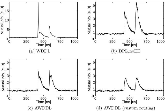
Performing the IT analysis using the mean and variance traces of each of our target designs led to the mutual information curves presented by Fig. 8. As expected, the WDDL design – due to its data-dependent time-of-evaluation and time-of-precharge – has the highest leakage. Interestingly the DPL noEE and the AWDDL designs have relatively the same amount of leakage in evaluation phase as they operate the same in this phase. However, DPL noEE has a higher leakage in the precharge phase. It indeed confirms our claim in Section 2 that due to the early propagation of DPL noEE in the precharge phase, in presence of imbalanced routings its leakage should be more easily detectable compared to that in the evaluation phase.
A comparison between the result of the AWDDL designs (routed by ISE vs. routed by our customized router) clearly shows the effectiveness of our developed router to reduce the information leakage. We should stress again that except the LUTs’ configuration all details and specification of the first three designs are the same, that allowed us to fairly compare these logic styles. The same holds for the two AWDDL designs which only differ in the routing of the AES S-box circuit.
Independent of the attack strategy, IT analysis captures the amount of in-formation available to the worst-case adversary. In order to quantify the data complexity (the number of required traces) of attacks on our target designs, we performed first-order profiling moments-correlating DPA [21]. Indeed, for each design profile we used a set of 100,000 profiling traces to estimate first-order moments, and made use of them as power models to perform a CPA attack on another set of 100,000 traces. The corresponding results are shown by Fig. 9. Thanks to the metric feature of moments-correlating DPA, we can directly con-clude the following ratios between the data complexity of the attack on different profiles:
0 250 500 750 1000 0
15
10
5
Time [ns]
Mutual Info. [e−3]
(a) WDDL
0 250 500 750 1000 0
1 2 3 4 5
Time [ns]
Mutual Info. [e−3]
(b) DPL noEE
0 250 500 750 1000 0
1 2 3 4 5
Time [ns]
Mutual Info. [e−3]
(c) AWDDL
0 250 500 750 1000 0
1 2 3 4 5
Time [ns]
Mutual Info. [e−3]
(d) AWDDL (custom routing)
Fig. 8.Mutual information curves for all profiles
– AWDDL versus DPL noEE: 00..0670542 = 1.5,
– AWDDL (custom routing) versus AWDDL: 00..0540382 = 2.0.
As a side note, though the leakage extractable from our AWDDL design is mitigated, it is not a perfect solution to prevent a key-recovery attack. There-fore – as it is well known – DPA-resistant logic styles, e.g., AWDDL, should be combined with other countermeasure such as algorithmic masking which usually cannot prevent DPA attacks when implemented in hardware [18].
5
Conclusions
0 250 500 750 1000 0
−0.05 0.10
Time [ns]
Correlation
0.111
(a) WDDL
0 250 500 750 1000
0
−0.05 0.05
Time [ns]
Correlation
0.067
(b) DPL noEE
0 250 500 750 1000
0
−0.05 0.05
Time [ns]
Correlation
0.054
(c) AWDDL
0 250 500 750 1000
0
−0.05 0.05
Time [ns]
Correlation
0.038
(d) AWDDL (custom routing)
Fig. 9.Result of first-order profiling moments-correlating DPA on all profiles
also be applied to similar logic styles or other applications requiring balanced routes, e.g., TRNGs and PUFs. It is noteworthy to mention that applying our customized router does not cause any area overhead. In fact, it only changes the way the routing resources (PIPs) are configured.
The only available source for delay of the signal routes is the ISE tool. There-fore, the effectiveness of a customized router relies on the conformity of ISE reports and the underlying FPGA chip. Due to the process variation as well as publicly unknown architecture of the FPGAs these numbers might be different from chip to chip or (even slightly) different to reality. Hence, as a future work, we plan to develop a mechanism to practically examine the differential delay as well as the power consumption of the dual-rail routings based on the target FPGA chip, where the design is supposed to be realized.
Acknowledgment
References
1. CryptoMiniSat. Available as download here https://gforge.inria.fr/frs/ ?group_id=1992.
2. Side-channel Attack Standard Evaluation Board (SASEBO). Further information are available viahttp://www.morita-tech.co.jp/SASEBO/en/index.html. 3. S. Bhasin, S. Guilley, F. Flament, N. Selmane, and J.-L. Danger. Countering early
evaluation: an approach towards robust dual-rail precharge logic. InWESS 2010, page 6. ACM, 2010.
4. D. Canright. A Very Compact S-Box for AES. In CHES 2005, volume 3659 of LNCS, pages 441–455. Springer, 2005.
5. Z. Chen and Y. Zhou. Dual-Rail Random Switching Logic: A Countermeasure to Reduce Side Channel Leakage. In CHES 2006, volume 4249 of LNCS, pages 242–254. Springer, 2006.
6. S. Guilley, P. Hoogvorst, Y. Mathieu, and R. Pacalet. The “Backend” Duplication Method. InCHES 2005, volume 3659 ofLNCS, pages 383–397. Springer, 2005. 7. T. G¨uneysu and A. Moradi. Generic Side-Channel Countermeasures for
Recon-figurable Devices. InCHES 2011, volume 6917 ofLNCS, pages 33–48. Springer, 2011.
8. W. He, E. de la Torre, and T. Riesgo. A Precharge-Absorbed DPL Logic for Reducing Early Propagation Effects on FPGA Implementations. In ReConFig 2011, pages 217–222. IEEE Computer Society, 2011.
9. W. He, A. Otero, E. de la Torre, and T. Riesgo. Automatic generation of identical routing pairs for FPGA implemented DPL logic. In ReConFig 2012, pages 1–6. IEEE, 2012.
10. C. Herbst, E. Oswald, and S. Mangard. An AES Smart Card Implementation Resistant to Power Analysis Attacks. InACNS 2006, volume 3989 ofLNCS, pages 239–252. Springer, 2006.
11. J.-P. Kaps and R. Velegalati. DPA Resistant AES on FPGA Using Partial DDL. InFCCM 2010, pages 273–280. IEEE Computer Society, 2010.
12. W. Klieber and G. Kwon. Efficient CNF Encoding for Selecting 1 from N Objects. InWorkshop on Constraints in Formal Verification - CFV, 2007.
13. P. C. Kocher, J. Jaffe, and B. Jun. Differential Power Analysis. InCRYPTO 1999, volume 1666 ofLNCS, pages 388–397. Springer, 1999.
14. C. Lavin, M. Padilla, J. Lamprecht, P. Lundrigan, B. Nelson, B. Hutchings, and M. Wirthlin. RapidSmith – A Library for Low-level Manipulation of Partially Placed-and-Routed FPGA Designs. Technical report, Brigham Young University, September 2012.
15. V. Lomn´e, P. Maurine, L. Torres, M. Robert, R. Soares, and N. Calazans. Evalu-ation on FPGA of triple rail logic robustness against DPA and DEMA. InDATE 009, pages 634–639. IEEE, 2009.
16. F. Mac´e, F.-X. Standaert, and J.-J. Quisquater. Information Theoretic Evaluation of Side-Channel Resistant Logic Styles. In CHES 2007, volume 4727 ofLNCS, pages 427–442. Springer, 2007.
17. S. Mangard, E. Oswald, and T. Popp. Power Analysis Attacks: Revealing the Secrets of Smart Cards. Springer, 2007.
19. A. Moradi, T. Eisenbarth, A. Poschmann, and C. Paar. Power Analysis of Single-Rail Storage Elements as Used in MDPL. InICISC 2009, volume 5984 ofLNCS, pages 146–160. Springer, 2009.
20. A. Moradi, M. Kirschbaum, T. Eisenbarth, and C. Paar. Masked Dual-Rail Precharge Logic Encounters State-of-the-Art Power Analysis Methods. IEEE Trans. VLSI Syst., 20(9):1578–1589, 2012.
21. A. Moradi and F.-X. Standaert. Moments-Correlating DPA. Cryptology ePrint Archive, Report 2014/409, 2014. http://eprint.iacr.org/.
22. D. E. Muller and W. S. Bartky. A Theory of Asynchronous Circuits. Report no. 78 at University of Illinois at Urbana-Champaign. Dept. of Computer Science, 1959. 23. M. Nassar, S. Bhasin, J.-L. Danger, G. Duc, and S. Guilley. BCDL: A high speed
balanced DPL for FPGA with global precharge and no early evaluation. InDATE 2010, pages 849–854. IEEE, 2010.
24. S. Nikova, V. Rijmen, and M. Schl¨affer. Secure Hardware Implementation of Non-linear Functions in the Presence of Glitches. J. Cryptology, 24(2):292–321, 2011. 25. E. Oswald, S. Mangard, N. Pramstaller, and V. Rijmen. A Side-Channel Analysis
Resistant Description of the AES S-Box. In FSE 2005, volume 3557 of LNCS, pages 413–423. Springer, 2005.
26. T. Popp, M. Kirschbaum, T. Zefferer, and S. Mangard. Evaluation of the Masked Logic Style MDPL on a Prototype Chip. InCHES 2007, volume 4727 ofLNCS, pages 81–94. Springer, 2007.
27. T. Popp and S. Mangard. Masked Dual-Rail Pre-charge Logic: DPA-Resistance Without Routing Constraints. InCHES 2005, volume 3659 ofLNCS, pages 172– 186. Springer, 2005.
28. L. Sauvage, M. Nassar, S. Guilley, F. Flament, J.-L. Danger, and Y. Mathieu. DPL on Stratix II FPGA: What to Expect? InReConFig 2009, pages 243–248. IEEE Computer Society, 2009.
29. F.-X. Standaert, T. Malkin, and M. Yung. A Unified Framework for the Analysis of Side-Channel Key Recovery Attacks. InEUROCRYPT 2009, volume 5479 of LNCS, pages 443–461. Springer, 2009.
30. D. Suzuki and M. Saeki. Security Evaluation of DPA Countermeasures Using Dual-Rail Pre-charge Logic Style. InCHES 2006, volume 4249 ofLNCS, pages 255–269. Springer, 2006.
31. K. Tiri, M. Akmal, and I. Verbauwhede. A dynamic and differential CMOS logic with signal independent power consumption to withstand differential power anal-ysis on smart cards. In Solid-State Circuits Conference - ESSCIRC 2002, pages 403–406, 2002.
32. K. Tiri and I. Verbauwhede. A Logic Level Design Methodology for a Secure DPA Resistant ASIC or FPGA Implementation. InDATE 2004, pages 246–251. IEEE Computer Society, 2004.
33. K. Tiri and I. Verbauwhede. Place and Route for Secure Standard Cell Design. In CARDIS 2004, pages 143–158. Kluwer, 2004.
34. R. Velegalati and J.-P. Kaps. Techniques to enable the use of Block RAMs on FPGAS with Dynamic and Differential Logic. InICECS 2010, pages 1244–1247. IEEE, 2010.
35. Xilinx. Virtex-5 Libraries Guide for HDL Designs. Available via
http://www.xilinx.com/support/documentation/sw_manuals/xilinx14_1/ virtex5_hdl.pdf, April 2012.