Available online:http://internationaljournalofresearch.org/ P a g e | 1227
Power optimization of dual modulus prescaler for higher
frequency using GDI technique
Eluri Shahanaz Begum Student* , [email protected]
Department of ECE,
Amrita sai institute of science and technology,Pariatala,Krishna dt ,Andrapradesh,India
P. Srinivas
Asst. professor, Department of ECE,
Amrita Sai institute of Science and Technology,Pariatala,Krishna dt ,Andrapradesh,India
Abstract: The coexistence of different
cellular system demands reconfigurable mobile terminals. For greater degree of application such as Text, graphics, audio and games etc are required to handle by modern handset. These demands can be
fulfilled by integrating some
Complementary technologies such as WLAN or Bluetooth, UWB for high bandwidth local or personal services and 2G — 3G standards for voice low data rate communication with wide area coverage together in same handset. Frequency dividers are useful in many communication
applications such as Frequency
synthesizers, Timing recovery circuits and clock generations. The design of frequency divider is an important factor in performance of PLL as it is in feedback path and so locking gets difficult.
Keywords: Keywords— High Operating Frequency, Minimum Power consumption, Minimum Area, Cmos Frequency Divider.
I INTRODUCTION
Prescaler is a critical block in power conscious PLL design. A new design technique that improves operating speed of true single-phase clock-based (TSPC) prescalers is presented. A reset signal is added to the positive edge
triggered TSPC DFF to obtain the objective of multi modulus prescaler that is frequency division (High frequency to low frequency). Two Dual-modulus prescalers 2/3 and 3/4 prescalers are designed using TSPC positive edge triggered DFF and CM OS nor gates. By using the two dual modulus prescalers, multi modulus prescaler is designed to provide multiple division ratios and their performances are compared with previous work. The speed of the 2/3 and 3/4 prescaler are improved at the maximum operating frequency. The power efficient multi modulus prescaler is designed using dsch tool and its performance are compared. A Simulation and measurement results shows high-speed, low-power, low PDP and multiple division ratio capa biIities of the power efficient technique. The improved speed, the power efficiency, and the flexibility will promote its wide deployment i n Multi gigahertz range applications.
Available online:http://internationaljournalofresearch.org/ P a g e | 1228 proposed design technique is applied to ÷2/3 and
÷3/4 prescalers, and their performances are compared with previous work. Implemented in a 130-nm CMOS technology and compared at same process-voltage-temperature conditions, the maximum speed of the ÷2/3 prescaler reaches 88% of the maximum operating frequency of a single TSPC flip-flop, and the ÷3/4 prescaler reaches 75%. In addition, the proposed divide-by-3 prescaler is able to work almost at the speed of the single TSPC flip-flop. A frequency divider that provides dividing ratios of 7, 8, and 9 is implemented as a part of a 3.4-5-GHz integer- Nphase-locked loop in a 65-nm CMOS technology. Simulation and measurement results demonstrate high-speed, low-power, and multiple division ratio capabilities of the proposed technique.
II. BACK GROUND
FIGURE 1:general diagram of
prescalar:
With the expanding need in terms of the low power consumption and increasing frequency of operation, CMOS has been the key element to fabricate the components. Also, the highest operating frequencies of prescalers implemented in GaAs and SiGe bipolar technologies have reached 5.4 GHz [3] and 3.6GHz [4]. Bipolar technologies do offer a high range of frequency of operation but at the expense of power consumption. So, to minimize the power is of prime importance. The prescaler block do consists of various submodules which comprises of nMOS and
pMOS. These transistors can be effectively used so as to reduce the area as well as the power consumption. The D flip Flop internal circuit is also shown here along with the
waveform and the power consumption has been brought to 5.4 gW. Compared with these, the prescalers fabricated in CMOS processes usually operate at lower frequencies. The highest reported operating frequency for CMOS prescalers is 1.5GHz [6], [7]. The circuit has been fabricated in a 65-nm technology and consumes relatively high power (115mW).Extra feedback networks were used [5] to increase the operating frequency to 5.4 GHz in a 0.18 gm CMOS process. A phase-shifting prescaler switches among signals with varying phases to achieve two or more divide ratios. The highest operating frequency for phase shifting prescalers [6] is 1.3 GHz and consumes 41 mW of power.
III. TSPC STRUCTURE:
.
Available online:http://internationaljournalofresearch.org/ P a g e | 1229 compared. Simulation and measurement results
show high-speed, low-power, low PDP and multiple division ratio capabilities of the power efficient technique with a frequency range of 1.0-5.8GHz. The improved speed, the power efficiency, and the flexibility will promote its wide deployment in Multi gigahertz range applications.
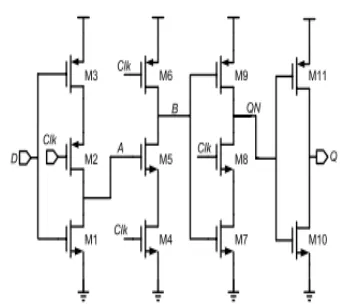
TSPC dynamic CMOS circuit is operated with one clock signal only to avoid clock skew problems. One reset signal is added with the TSPC circuit. Fig.1. below shows the TSPC flip-flop with reset. This TSPC circuit is used in the 2/3 and 3/4 prescaler. Fig.2. below shows the symbol of TSPC positive edge triggered d flip-flop. This symbol is used in 2/3 prescaler and 3/4 prescaler designs.
1V EXISTING CIRCUIT DIAGRAM:
PROPOSED 16/17 PRESCALAR:
In the transistor level forward body biasing technique can improve the speed by decreasing threshold voltage of nmos transistors.How ever it suffers from high minimum working frequency as well as increased cost decreased robustness. A divide counter (M) is inserted in the feedback loop to increase the VCO frequency above the input reference frequency.Dynamic logic multiband flexible
integer-n divider based on pulse-swallow topology uses a low-power wideband 2/3 prescaler and a wideband multi modulus 16/17 prescaler .The divider also uses an improved low power loadable bit-cell for the Swallow S-counter.Saves a considerable amount of power and also reduces the complexity of multi band divider. Here the clock divider uses a wide band 2/3 prescaler and a multimodulus prescaler.
As well as the conventional circuit, the maximum working frequency of proposed prescaler is decided by its divide-by-17 operation mode. In addition, the key operation in divide-by-17 mode is the divide-by-3 operation of pseudo divide-by-2/3 prescaler. Fig. 4 shows the timing diagram of this key operation of proposed circuit. In the first rising edge of Fin, QN1 and QN2 switch to high, then MC1 switches to high and holds for two periods. In the second rising edge,QN0 and D1 switch to low for two periods. In the third rising edge, QN1 switches to high and holds for two periods. From the second to the fifth rising edge of Fin, DFF1 outputs a divide-by-3 signal in node QN1 and the pseudo divide-by-2/3 prescaler accomplishes a divideby-3 operation. After this, the pseudo divide-by-2/3 prescaler will carry out seven times divide-by-2 operation. A divide-by-17 signal will be obtained in node Fout.
Available online:http://internationaljournalofresearch.org/ P a g e | 1230 to the input CLK node of DFF2, DFF3, and
DFF4, respectively. The propagation delay of DFF1, DFF2, and DFF3 will all
decrease from td− Q to
td−QN. Thus, the length of critical path will be further reduced.
The operation mode of proposed circuit is as follows. When MC = 1, MC1 changes its value according to (QN2, QN3, QN4).The pseudo divide-by-2/3 prescaler controlled by MC1 accomplishes seven times of divide-by-2 operations and one time of divide-by-3 operation in a cycle. The whole circuit operates in divide-by-17mode. When MC = 0, MC1 keeps low and the pseudo divide-by-2/3 prescaler keeps on divide-by-2 operation. The whole circuit works in divide-by-16 mode.
V. PROPOSED TSPC D FLIPFLOP:
Figure for tspc dflipflop:
GDI TECHNIQUE:
GDI (Gate Diffusion Input) - a new technique of low power digital circuit design is described. This technique allows reducing power consumption, delay and area of digital circuits, while maintaining low complexity of logic design. Performance comparison with traditional CMOS and various PTL design techniques is presented, with respect to the layout area, number of devices, delay and power dissipation,
showing advantages and drawbacks of GDI as compared to other methods. A variety of logic gates have been implemented in 0.35 μm technology to compare the GDI technique with CMOS and PTL. A prototype test chip of 8-bit CLA adder has been fabricated, based on GDI and CMOS cell libraries, showing up to 45% reduction in power-delay product in GDI.
AND GATE USING GDI TECHNIQUE:
From the above figure,by using gdi technique we can reduce the area and power consumption.such that the overall power consumption can be reduced.
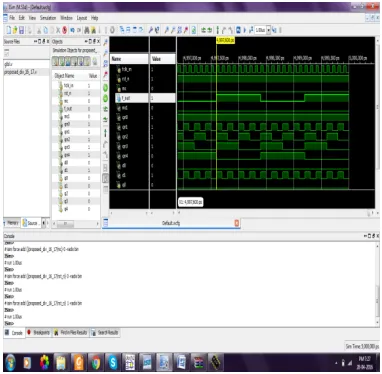
V1.simulation results:
Available online:http://internationaljournalofresearch.org/ P a g e | 1231
Simulation results in microwind tool
Layout for proposeed circuit:
Power consumption for existing system:
Power consumption for proposed system:
VI1 APPLICATION:
The major applications of frequency dividers are mainly used inFor greater degree of application such as Text, graphics, audio and games etc are required to handle by modern handset. These demands can be fulfilled by integrating some Complementary technologies such as WLAN or Bluetooth, UWB for high bandwidth local or personal services and 2G — 3G standards for voice low data rate communication with wide area coverage together in same handset. Frequency dividers are useful in many communication applications such as Frequency synthesizers
VIII CONCLUSION:
By using gdi technique and tspc flipflop with 9 transistors can reduce the power consumption of the circuit.hence we can design frequency dividers such as 31/32,127/128 and so on with less power consumption.hence this can be helpful.
REFERENCES
1. Sudheer Kumar Yezerla, B Rajendra Naik, “Design and Estimation of delay, power and area for Parallel prefix adders” 978-1-4799-2291-8/14/$31.00 ©2014 IEEE, Proceedings of 2014 RAECS UIET Panjab University Chandigarh, 06 - 08 March, 2014 2. David H.K.Hoe, Chris Martinez and
Available online:http://internationaljournalofresearch.org/ P a g e | 1232 Prefix Adders using FPGAs”, 2011
IEEE 43rd Southeastern Symposium in pp. 168-172, 2011. 3. N. H. E. Weste and D. Harris,
CMOS VLSI Design, 4th edition, Pearson–Addison Wesley, 2011. 4. R. P. Brent and H. T. Kung, “A
regular layout for parallel adders,” IEEE Trans. Comput., vol. C-31, pp. 260-264, 1982.
5. D. Harris, “A Taxonomy of Parallel Prefix Networks,” in Proc. 37th Asilomar Conf. Signals Systems and Computers, pp. 2213–7, 2003. 6. P. M. Kogge and H. S. Stone, “A
Parallel Algorithm for the Efficient Solution of a General Class of Recurrence Equations,” IEEE Trans. On Computers, Vol. C-22, No 8, August 1973.
7. D. Gizopoulos, M. Psarakis, A. Paschalis, and Y. Zorian, “Easily Testable Cellular Carry Lookahead Adders,” Journal of Electronic Testing: Theory and Applications 19, 285-298, 2003.
8. T. Lynch and E. E. Swartzlander, “A Spanning Tree Carry Lookahead Adder,” IEEE Trans. on Computers, vol. 41, no. 8, pp. 931-939, Aug. 9. Beaumont-Smith, A, Cheng-Chew
Lim ,”Parallel prefix adder design”, Computer Arithmetic, 2001. Proceedings. 15th IEEE Symposium,pp. 218 – 225,2001.M. Young, The Technical Writer's Handbook. Mill Valley, CA: University Science, 1989
10. K. Vitoroulis and A. J. Al-Khalili, “Performance of Parallel Prefix Adders Implemented with FPGA technology,” IEEE Northeast Workshop on Circuits and Systems, pp. 498-501, Aug. 2007. 172.
11. S. Xing and W. W. H. Yu, “FPGA Adders: Performance Evaluation and Optimal Design,” IEEE Design & Test of Computers, vol. 15, no. 1, pp. 24-29, Jan. 1998
12. Raghava Garipelly, P.Madhu Kiran,
A.Santhosh Kumar,“A Review on Reversible Logic Gates and their Implementation”, ISSN 2250-2459, ISO 9001:2008 Certified Journal, Volume 3, Issue 3, March 2013 13. Prashant .R.Yelekar, Sujata S.
Chiwande, “Introduction to Reversible Logic Gates & its Application”, 2nd National Conference on Information and Communication Technology (NCICT) 2011 Proceedings published in International Journal of Computer Applications® (IJCA) 14. Manjeet Singh Sankhwar, Rajesh
Khatri, “Design of High Speed Low Power Reversible Logic Adder Using HNG Gate”, Int. Journal of Engineering Research and Applications, ISSN : 2248-9622, Vol. 4, Issue 1( Version 2), January 2014, pp.152-159
15. Madhusmita Mahapatro, Sisira Kanta Panda, Jagannath Satpathy, Meraj Saheel, “Design of Arithmetic Circuits Using Reversible Logic Gates and Power Dissipation Calculation”,978-1-4244-8979-4©2010 IEEE, Electronic System Design (ISED), 2010 International Symposium 16. Zhijin Guan, Wenjuan Li, Weiping
Ding, Yueqin Hang, “An Arithmetic Logic Unit Design Based on Reversible Logic Gates”, 978-1-4577-0253-2/11/$26.00 ©2011 IEEE
17. J.W.Bruce, M.A.Thornton, L.Shivakumaraiah, P.S.Kokate, X.Li, “Efficient adder circuits based on a conservative reversible logic gate”, Proceedings of the IEEE Computer Society Annual Symposium on VLSI (ISVLSI.02), 0-7695-1486-3/02 $17.00 © 2002 IEEE
Available online:http://internationaljournalofresearch.org/ P a g e | 1233 Symposium on VLSI, New
Frontiers in VLSI Design, 0-7695-2365-X/05 $20.00 © 2005 IEEE 19. Zhijin Guan, Wenjuan Li, Weiping
Ding, Yueqin Hang,”An Arithmetic Logic Unit Design Based on Reversible Logic Gates”, 978-1-4577-0253-2/11/$26.00 ©2011 IEEE
20. Lekshmi Viswanath, Ponni.M,” Design and Analysis of 16 Bit Reversible ALU”, IOSR Journal of Computer Engineering (IOSRJCE) ISSN : 2278-0661 Volume 1, Issue
1 (May-June 2012), PP 46-53 21. R. Landauer, “Irreversibility and
Heat Generation in the Computational Process”, IBM Journal of Research and Development, 5, pp. 183- 191, 1961.
22. C H Bennett, "Notes on the History of Reversible Computation", IBM Journal of Research and
Development, vol. 32, pp. 16-23, 1998.