Using Parametric Design to Reduce the EMI of Electronics Products
— Example of Medical-Grade Touch Panel Computer
Chien-Yi Huang1, *, Ching-Hsiang Chen2, and Christopher Greene3
Abstract—With technical advancement and development, the amount of electronic equipment is increasing, while the functions of products are enhanced, and the routing density of Printed Circuit Boards (PCBs) becomes larger. In the electronic industry, medical instruments are used to diagnose, treat, mitigate or prevent human diseases, and maintain and promote health. Industrial PCs for medical use and their accessories should be immune to interference from external electromagnetic noise, and should not become interference sources of electromagnetic noise radiation, so they have become issues of interest with respect to ensuring safety of medical equipments in medical operation environments in recent years.
This research relates to parametric design using the Taguchi Method in the early stage of product development for medical-grade touch panel computers. In considering the use of Radiated Emission (RE) in Electromagnetic Compatibility (EMC) as a response value, the experiment covers control factors such as PCB and mechanism design related parameters. In addition, peripheral devices used in conjunction with a product are considered as noise factors when the product is in use, while interaction between the control factors is studied. The Taguchi Method is used to select an appropriate inner/outer orthogonal array, and a response diagram and a variance method are used for analysis to provide an optimal set of design parameters, in which the number of routing layers of a riser card is 6; the EMI filter on the isolated card is 600 Ω; the shunt capacity for the clock on main board is 33p; and the isolated card is grounded. Moreover, it is found that an interaction exists between the number of routing layers of the riser card and the EMI filter of the isolated card. From the result of the experiment, with such a set of parameters, the SN (Signal to Noise Ratio) lies in the confidence interval, indicating good reproducibility of the experiment. Such a parametric design effectively improves the electromagnetic interference (EMI) characteristics of a product to meet design specifications required by customers, accelerate the R&D process of electronic products, and pass EMI test regulations required by various countries in order to improve industrial competitiveness.
1. BACKGROUND AND MOTIVATION OF THE RESEARCH
The Industrial PC (IPC) was first used in factory automation to act as a CNC (Computer Numerical Control) and as the control core of machines, such as a CNC lathe, capable of monitoring, controlling or testing machines or instruments in manufacturing process. With advanced techniques and more convenience required by human beings in life, its new application has gradually been oriented to industrial automation and life automation. In additional to the manufacturing industry, computer automation control is currently used in the financial sector, telecommunication network industry, and even medical care and monitoring.
Received 18 September 2018, Accepted 28 November 2018, Scheduled 12 December 2018 * Corresponding author: Chien-Yi Huang ([email protected]).
From the medical industry’s position in people’s welfare, the scope of the medical service market is extending, including various medical care related industries, such as the traditional hospital industry, pharmaceutical industry, and emerging biotech industry. Generally, the medical industry refers to industries/institutions regarding prevention, examination, treatment, rehabilitation, nursing and care for physical and mental health and disease, including manufacturers and suppliers of medical devices, manufacturers and dealers of various medicines, as well as various people working in various medical institutions, such as hospitals/clinics, inspection stations, and nursing homes.
In the electronic industry, medical instruments are used to diagnose, treat, mitigate or prevent human diseases, and maintain and promote health. Medical devices feature a diverse set of products, high technical complexity and integration, high margins, high uncertainty of R&D and profit, as well as a high closure of market, etc. However, Small Medium Enterprises (SMEs) play a main role in the medical device industry in Taiwan, and traders are mainly import oriented. Production, manufacturing and channels have been increased in recent years. Since the domestic market is small, and finished products are mainly export oriented, raw materials are mainly sourced overseas. Most manufacturers are assembly Original Equipment Manufacturers (OEMs) based on production technology, and most products are social welfare devices.
The amount of electronic equipment is increasing, while the functions of products are enhanced, and the routing density of Printed Circuit Boards (PCBs) becomes larger [1, 12, 18]. Further, the clock rate of the Central Process Unit (CPU) is becoming faster, so that the operating frequency tends to high frequency. Crosstalk issues will appear accordingly to cause Electromagnetic Interference (EMI), coupling signals and time delays, such that normal functions of the product are influenced in operation. Medical equipment with reversible interference issues can result in faulty diagnosis or treatment.
The accuracy of EMI/EMC measurement depends on many factors, including whether the measurement environment is qualified, whether the measurement instrument is standard, whether the electromagnetic coupling between the measurement instrument and the Equipment Under Test (EUT) is eliminated, whether artificial operation procedure is correct, etc. There are standard regulations or international certifications for many existing EMI/EMC measurement procedures, environments, instruments, etc. In recent years, advanced countries, such as USA, Japan and the European Union (EU), have proposed regulations for EMI levels generated by electronic products, together with control, successively in order to protect radio communication and computer information control. For example, regulations such as the Federal Communications Commission (FCC) of USA, Voluntary Control Council for Interference (VCCI) of Japan, Communate Europpene (CE) mark of European Union (EU) and C-tick of Australia require that electronic information products which are to be imported shall apply and be tested to be qualified prior to legal transportation and sale. The Bureau of Standards, Metrology and Inspection (BSMI) has also implemented control measures since 1996 in our country.
As for hand phone, notebook, as well as medical devices emit electromagnetic fields (EMF), these emissions are a risk exposure for the human beings in the proximities due to the energy that is absorbed by tissues. In these conditions, the specific absorption rate (SAR) is defined as the amount of energy absorbed by tissues. Factors affecting the amount of absorbed energy are features of the wave, features of the body, and also environmental features. About the features of the wave, the SAR depends on the features of the signal emitted by the radiation source, such as frequency [14] and polarization [11]. About the dependence with the body, the SAR depends on the type of tissue, the posture of the body [22], frontal or back incidence [10], etc. Accordingly, before selling products to domestic or overseas markets, in most cases domestic electronic companies cannot pass the EMI test standards required by the regulations of client countries, so that the time to market is delayed, and business opportunities are lost significantly.
and improvement approaches in the aspects of theory research and design in order to improve EMI by blocking the interference path to suppress interference, and by using grounding, shielding, filtering and PCB layout. Colotti [8] indicated that EMI is formed due to three keys, including an interference source, coupling path and interfered susceptor, and EMI issues are mitigated by reducing the noise of the interference source, or developing and maintaining relevant control plans. However, the research above is only limited to explanation of theory without describing countermeasures and introductory methods which improve EMC effectively in detail for specific products or regulations.
In references, scholars also used masking approaches to reduce EMI noise. Lin et al. [19] set forth the EMI masking characteristic of methyl vinyl silicone composite materials with bamboo-like carbon nanotubes of different concentrations. However, the concentration of liquid cannot be controlled easily, so the conductivity is influenced, thereby reducing the effectiveness of masking. Zhao et al. [26] proposed independent cables and motors for evaluating the EMC design of one converter and simplified different model constructions/configurations to execute this verified hypothesis. Moreover, some scholars studied grounding. Researchers used grounding approaches to reduce EMI noise [6]. Liu [20] studied and controlled EMI due to a grounding loop, which is increased with the complexity of system. In this research, EMI is reduced by eliminating the grounding loop and limiting its area. However, harmonic waves due to the oscillator (crystal) cannot be eliminated by this approach.
The scholar below reduces EMI noise by using a filtering approach [21]. Aksoy [3] proposed design of an EMI power line filter, which filters out transient signals coupled to military system power lines, and conducted and radiated noise generated by the switched mode power supply. However, a common mode choke with a large volume and occupied space was used as the inductive component to suppress low frequency noise in this research, so it is not applicable to products with limited space.
In references, the number of routing layers of PCB was proposed to suppress EMI noise [9, 17]. In this research, multilayer is mainly studied, in order to increase the area for routing, increase functional density and reduce EMI. In a multilayer PCB, the entire layer is connected to the ground line and power directly. Layers are classified into signal layer (Signal), power layer (Power) and ground line layer (Ground). In the case that different power supplies are required for parts on a PCB, such a PCB usually has two or more power and wire layers. Huang & Chen [13] studied an industrial panel display, and electromagnetic fields and electromagnetic waves may result in an adverse influence for peripheral equipment in use to malfunction, resulting in system failure or unintentional accidents and inducing worry of severe public safety incidents. The three EMC characteristics, including RE, conduction interference and fast transient impulse immunity of power, are considered response values; control factors are determined with respect to relevant parameters for PCB and mechanism design of the product; and peripheral devices used in conjunction with the product are considered as noise factors. Grounding in PCB routing design with EMI is studied to reduce design cost and reduce the influence of EMI and ESD.
In order to meet the requirements of medical-grade computers, riser cards are mounted on the main boards additionally for transmitting signals to isolated cards through riser cards. The purpose is to meet the requirements that medical products have to be connected with various peripheral devices. Thus, connection ports are additionally arranged on the isolated card [7]. Since electrostatic discharge or surges may occur for external devices, grounded regions of the main board and isolated card are isolated to prevent the main board from being impacted [5, 23]. However, EMI issues for the noise of the isolated cad cannot be reduced through grounding, so it is more difficult to pass the regulation test.
1.1. Purpose of the Research
This research is intended to propose countermeasures which reduce EMI for medical-grade touch panel computers in order that such electronic products can meet relevant standards and regulations.
(1) For EMI test standards required by regulations, influences of parameters (i.e., control factors) with respect to circuit board and mechanism are considered systematically. Even though the products can fit external factors, such as end customers in different service environments and different countries, the influence of noise variation may result.
conduct the experiment. Data analysis is used in conjunction to determine the optimal set of parametric designs, in order to suppress EMI effectively and to meet design specifications required by customers, such that EMI test regulations stipulated by various countries for products can be passed quickly.
(3) They are provided to operation/management decision makers as reference for the direction of product design. EMI issues can be considered in the early stage of product design to reduce countermeasure components, product cost and labor consumption due to a number of design changes in the R&D cycle, and to accelerate the R&D process.
Studying the Interaction Which Might Exist Between
the Control Factors
Description of Product
Defining Response Values, Control Factors
and Noise Factors
Determining an Orthogonal Array and Conducting
Configura tion
Determining Test Environment
Conducting Experiment
Determining Factor Significance and the Optimal
Set of Parameter Levels
Experiment Verification
Response Diagram ANOVA Calculation of SN Ratio
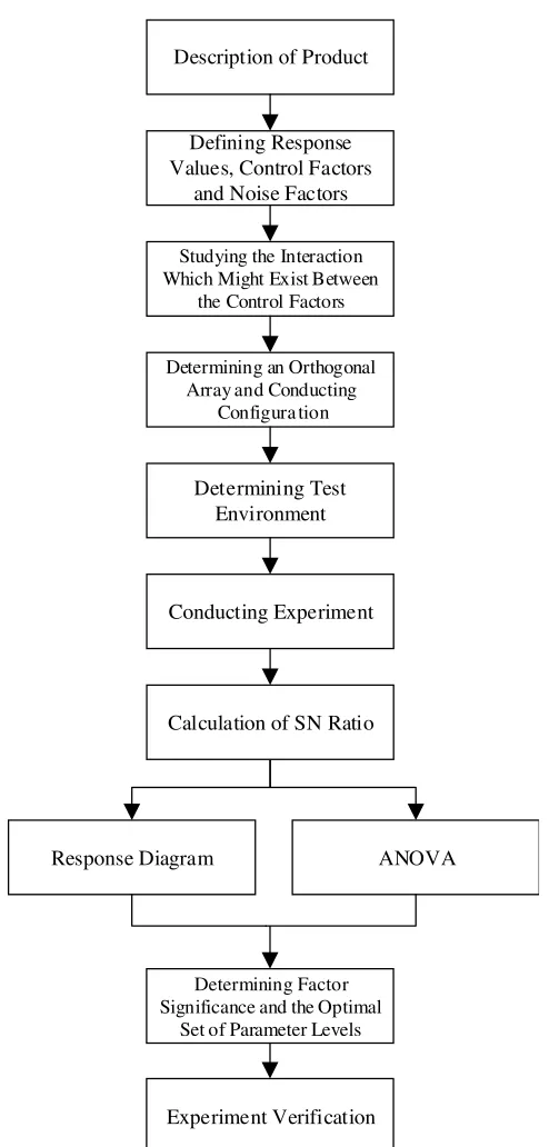
1.2. Research Process
In this research, the EMI of electronic products is studied for medical-grade touch panel computers. First, important parameters are filtered through engineering knowledge, such as electronics, electrical machinery, mechanisms, and PCB routing design. The quality characteristics (response values) for measuring EMI and the control factors and noise factors which influence EMI are determined, and the interaction which might exist between the control factors is studied. The Taguchi Method is used to select the appropriate orthogonal array, linear graph and configuration of the experiment. Next, the test environment is identified, and the experiment is conducted to obtain data, which is converted into the signal to noise ratio (SN ratio). A response table and a response diagram are used to determine the influence of various factors in different levels, followed by conducting Analysis of Variance (ANOVA) to determine factor significance, and the optimal set of parameters is provided. Lastly, a verification experiment is executed to ensure the effectiveness of the result. The research process is as shown in Figure 1.
2. DESCRIPTION OF PRODUCT
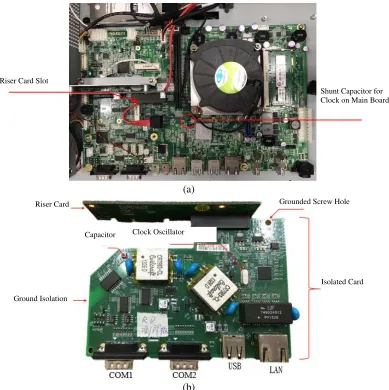
In this research, a medical-grade touch panel computer is studied, in which a main board and a circuit board of the product are as shown in Figure 2. Such a product is widely used for medical and commercial
Shunt Capacitor for Clock on Main Board Riser Card Slot
Riser Card
Capacitor
Grounded Screw Hole
Clock Oscillator
Ground Isolation
Isolated Card
(b) (a)
purposes, mainly to monitor information, such as conditions of patients, external connection to other medical equipment, patient records and physical conditions. It seems to have become the main stream in the market due to its high return and high gross margin. Such a product has to accommodate specially designed models of circuit boards and components to achieve high performance operation and may be used in an environment regarding artificial life safety, etc.
3. EXPERIMENT PLANNING
This research relates to parametric design using the Taguchi Method in the early stage of product development for medical-grade touch panel computers. In consideration of the use of radiated emission in electromagnetic compatibility as response values, the experiment covers control factors such as PCB and mechanism design related parameters. In addition, peripheral devices used in conjunction with a product are considered as noise factors when the product is in use, while interaction between the control factors is studied.
3.1. Response Values
EMC means that one device can have its emitted EMI limited without influencing the normal operation of peripheral systems, while resisting external noise and operating normally in an electromagnetic environment. Thus, it includes two characteristics, including EMI and EMS. In this research, the radiated emission which may influence normal operation of a product by a medical-grade liquid crystal computer during use is considered as a response value, test environment and data collection for the experiment as described below:
Radiated Emission (RE) (dB): It means that the electromagnetic noise is radiated and propagated through a space in the form of electromagnetic field energy, and coupled to interfered devices (or their circuits) [24, 25]. Noise of various frequencies may be generated in the EMI measurement of a product. In this research, the noise with the highest frequency is selected, and the noise measurement value acts as a response value. The smaller the value is, the lower the RE level is, so it belongs to the Smaller The Better (STB) characteristic of Taguchi quality.
3.2. Control Factors
In this research, the important parameters related to PCB and mechanism designs of a medical-grade touch panel computer are considered as the control factors of the experiment, and the selection reasons and their levels are described as following:
A. “Number of Routing Layers on Riser Card”: The number of layers can influence product characteristics, including functional density, EMI, product size and cost. The larger the number of layers is, the more helpful it is for isolating noise, that is, for reducing EMI. In this research, two levels of layer numbers are considered for riser cards, including a 4-layer board and a 6-layer board. B. “EMI Filter on Isolated Card”: The filter technique allows signal frequencies required in design to pass, while unnecessary noise frequencies are degraded to suppress noise interference. In order to avoid common mode impedance coupling due to the pickup of noise when being provided for various IC powers, ferrite bead suppression components are added at the entrance where the power enters the IC on PCB, thereby filtering out high frequency interference of the local circuit. In this research, a ferrite bead inductor is provided at the entrance mentioned above where power enters IC. Two resistance levels of inductor are considered, including 0 Ω and 600 Ω.
C. “Clock Shunt Capacitor Component”: The clock component and capacitor component are designed in parallel connection on the main board to increase the capacity and storage charges. Moreover, adding a capacitor may reduce the radiation of the current loop to suppress noise. In this research, two levels are considered for the capacitor, including 0p and 33p.
such that the influence of static electricity will not occur easily when being contacted by the human body, and sparks will not be caused inside the equipment. In this research, two levels are considered, including that without grounding and that with grounding.
3.3. Second Order Interaction
PCB design and electronic component characteristics are considered. In the research, the second order interactions between the following three sets of control factors will be studied:
(1) “Number of Routing Layers on Riser Card” and “EMI Filter on Isolated Card”: The influence of resistance of the EMI filter on the isolated card on the magnitude of electromagnetic noise may vary with the number of routing layers on the riser card.
(2) “Number of Routing Layers on Riser Card” and “Shunt Capacitor for Clock on Main Board”: The influence of resistance of the shunt capacitor for the clock on the main board on the magnitude of electromagnetic noise may vary with the routing layers on the riser card.
(3) “Number of Routing Layers on Riser Card” and “Grounding of Isolated Card”: The influence of grounding of the isolated card on the magnitude of electromagnetic noise may vary with the number of routing layers on the riser card.
3.4. Noise Factors
The level of noise which may be influenced by peripheral devices in conjunction with the product during use is considered. For example, connection wires and their placement may all generate different levels of EMI. Thus, the following noise factors are considered in this research:
E. “Switching Power Supply”: Switching power supply uses high frequency switching technology of semiconductor switches, for which common mode noise is the main noise source. Most such products are provided by suppliers, and their EMI levels may differ. In this research, 5-stage and 4-stage power suppliers are considered, with power efficiencies of 92% and 95%, respectively. Less stages indicate more saved power and higher energy efficiency.
F. “Signal Cable Filter”: As an electronic product is connected with a peripheral device, a signal line may bring out and emit noise to air, forming an interference noise source. Most manufacturers add a ferrite core filter when a signal line is close to the EMI originator. As the signal line passes through the ferrite core (Figure 3), a signal may pass through effectively with almost no degradation, while interference noise is blocked and converted into heat, which is dissipated, such that noise is filtered and transmission quality of the signal improved. In this research, two numbers of signal line filters are considered, including 1 core and 2 cores.
(b) (a)
Figure 3. Signal line with added immunity magnetic ring. (a) 1 core. (b) 2 cores.
USA/Canada; 240 V/50 Hz (C-TICK) is used in Australia; and 230 V/50 Hz (CE) is used in Europe, while the used voltage may influence EMI level. Since Europe and the USA are the key sales markets, two test voltage/frequency levels are considered, including 120 V/60 Hz and 230 V/50 Hz.
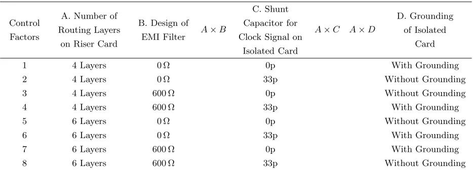
3.5. Configuration of Orthogonal Array
In this research, an L8(27) inner orthogonal array is built, and the second-order interaction which may exist between the control factors mentioned above is considered. In this experiment, four 2-level factors (A,B,C,D) are considered, and the second-order interactions,A×B,A×CandA×D, are evaluated. The L8 orthogonal array and standard point plot are as shown in Table 1 and Figure 4. In turn, noise factors (Table 2) are considered in conjunction with an L4(23) outer orthogonal array to ensure that the optimal set of control factor parameters is applicable to various noise factor sets.
Table 1. Experimental configuration of the L8 control factors.
Control
Factors
A. Number of Routing Layers
on Riser Card
B. Design of
EMI Filter A×B
C. Shunt
Capacitor for
Clock Signal on Isolated Card
A×C A×D
D. Grounding of Isolated
Card
1 4 Layers 0 Ω 0p With Grounding
2 4 Layers 0 Ω 33p Without Grounding
3 4 Layers 600 Ω 0p Without Grounding
4 4 Layers 600 Ω 33p With Grounding
5 6 Layers 0 Ω 0p Without Grounding
6 6 Layers 0 Ω 33p With Grounding
7 6 Layers 600 Ω 0p With Grounding
8 6 Layers 600 Ω 33p Without Grounding
Figure 4. Linear graph ofL8 interaction.
Table 2. Experimental configuration of the L4 noise factors.
Noise Factors E. Switching
4. TEST ENVIRONMENT AND DATA COLLECTION
In the research, Radiated Emission (RE) generated by a medical-grade touch panel computer during use is considered and described as follows:
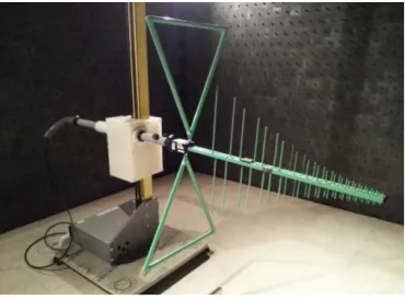
RE: The instrument/equipment includes a test receiver (EMI test receiver), a wireless (radio frequency; RF) cable, a monopole biconical antenna (Figure 5), an antenna elevation unit, and an Equipment Under Test (EUT) rotation disk with a frequency ranging from 30 to 1000 MHz. The test site is a semi-anechoic chamber with a dimension of 7 m (length) × 4 m (width) × 3 m (height). In measurement, the distance between the EUT and the antenna is 3 m. The EUT is placed on a non-conductive table with a height of 80 cm and is located on a 360-degree rotational disk, while the antenna is elevated at a height of 1–3 m. An electromagnetic wave signal is transmitted outside the laboratory through the coaxial cable. The signal is amplified by a low noise preamplifier, followed by being transmitted to a spectrum analyzer for observation in order to discover the maximum radiation measurement value (Figure 6).
Figure 5. Monopole biconical an-tenna.
Figure 6. Architecture diagram of RE test.
In the research, the test condition of EN60601 radiation class B, an international EMI test regulation, is referenced. For a test environment with an enclosed space, upper bounds of 40 dB and 47 dB are allowed for frequency bands between 30 MHz and 230 MHz, as well as between 230 MHz and 1000 MHz. In an upfront experiment, two antenna erections are considered, including the erection in which an antenna is horizontal to ground surface and the erection in which an antenna is vertical to ground surface. The antenna is tuned to heights of 1 m, 1.4 m and 1.8 m, respectively, together with a 360-degree rotation of the rotation disk to collect the maximum noise radiation value. From the result, in the horizontal test, the maximum measurement value is over a limit of 7.585 dB at a frequency of 99.84 MHz, while in the vertical test, the maximum measurement value is below a limit of 5.073 dB at a frequency of 165.8 MHz. Further, the noise measurement values under the antenna height conditions mentioned above are compared. From the result, the highest radiation level occurs at 1.8 m. Thus, the worst case scenario with the highest noise interference level is selected in this research, i.e., the vertical test and the antenna height of 1.8 m with a frequency of 165.8 MHz are adopted as the measurement conditions for subsequent experiments, in order to ensure that the data are obtained in the worst case scenario.
5. DATA ANALYSIS
5.1. Factorial Effect Analysis
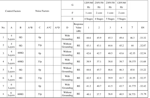
The experimental data are as shown in Table 3. Since RE level belongs to the Smaller The Better (STB) characteristic of Taguchi quality, Formula (1) is used to calculate SN ratios under various parameter sets. Averages of SN ratios for various control factors at various levels are calculated, and a response table and a response diagram as shown in Table 4 and Figure 7, respectively, to show levels of influence of various factors on the quality characteristic (SN). From the results, the optimal set of parameter levels for EMI reduction is: the number of routing layers on riser card is 6; the EMI filter on the isolated card is 600 Ω; the shunt capacity for the clock on the main board is 33p; and the isolated card is grounded, in order to obtain a smaller RE.
SNST B =−10 log
1 n n i=1 y2 i (1)
whereyi is the ith measurement value, andn is the number of samples (n= 4).
Table 3. Configuration of inner/outer orthogonal array and experimental result for EMC parametric design. Noise Factors G 120V/60 Hz 230V/50 Hz 230V/50 Hz 120V/60 Hz
F 1 core 2 core 1 core 2 core Control Factors
E 4 Stages 4 Stages 5 Stages 5 Stages
No. A B A*B C A*C A*D D
Response Value
(dB)
1 2 3 4 SN
1 Layers 4 0Ω 0p With
Grounding RE 44.6 45.9 45.3 49.4 46.3 -33.32
2 Layers 4 0Ω 33p Grounding Without RE 43.1 43.1 44.6 45.2 44 -32.87
3 4
Layers 600Ω 0p
Without
Grounding RE 42.6 42.7 40.5 43.6 42.35 -32.54
4 4
Layers 600Ω 33p
With
Grounding RE 38.9 37.1 38.8 38.7 38.375 -31.68
5 6
Layers 0Ω 0p
Without
Grounding RE 44.6 45.7 46.6 46.3 45.8 -33.22
6 6
Layers 0Ω 33p
With
Grounding RE 42.5 42.1 39.9 41.7 41.55 -32.37
7 6 0p With RE 41.2 40.7 41.5 43.7 41.775 -32.42
y 8 Layers Grounding -600Ω 6 Layers 33p Without
Grounding RE 40.1 37.7 36.8 40.5 38.775 31.78
5.2. ANOVA of Taguchi Quality
Table 4. Response table for SN ratio of RE parameter set.
Control Factors
A. Number
of Routing Layers on
Riser Card
B. EMI Filter on
Isolated Card
C. Shunt Capacitor For Clock on Main
Board
D. Grounding of Isolated
Card
RE Level 1 −32.60 −32.95 −32.87 −32.45 Level 2 −32.45 −32.11 −32.18 −32.60 Full Range 0.155 0.8399 0.6983 0.1528
Rank 3 1 2 4
Figure 7. Response diagram for SN ratio of RE parameter set.
Main Board”. The result is consistent with the analysis result of factorial effect. Accordingly, electronic circuit design engineers of products are recommended to reserve an Inductance-capacity circuit (LC circuit) for the purpose of suppressing EMI.
Moreover, A×B (i.e., “Number of Routing Layers on Riser Card” and “EMI Filter on Isolated Card”) is more significant than other interactions. Its interactions are as shown in Figure 8. It is known that the improvement for magnitude of electromagnetic noise is more significant by adding “EMI Filter on Isolated Card” as the “Number of Routing Layers on Riser Card” is 4 because the suppression effect for electromagnetic noise has been achieved as the number of routing layers is 6, and thus the effect of further improvement is limited to the installation of a filter.
Table 5. Response table for various control factors and their interactions.
A B
A×B
C
A×C A×D
D
Control Factors
Number of Routing Layers on
Riser Card
EMI Filter on Isolated
Card
Shunt Capacitor For Clock on Main
Board
Grounding of Isolated
Card
RE
Level 1 −32.60 −32.95 −32.60 −32.87 −32.50 −32.50 −32.45 Level 2 −32.45 −32.11 −32.45 −32.18 −32.55 −32.55 −32.60
Table 6. ANOVA for SN ratio of RE.
Freedom Sum of Squares
Mean
Square F Value
Net Sum of Squares
Contribution
Rate (%) P-Value
A 1 0.0481 0.0481 9.9728 0.0433 1.90% 0.087
B 1 1.4107 1.4107 292.6535 1.4107 55.72% 0.003
C 1 0.9753 0.9753 202.3269 0.9753 38.53% 0.005
D 1 0.0467 0.0467 9.6857 0.0467 1.84% 0.090
A∗B 1 0.0412 0.0412 8.5437 0.0412 1.63% 0.100
Error 2 0.0096 0.0048 0.38%
Total 7 2.5316
Figure 8. Diagram showing interaction of SN ratios for “number of routing layers on riser card” × “EMI filter on isolated card”.
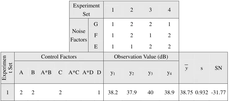
5.3. Experiment Verification
Experiment verification is executed for A2B2C2D1, the optimal parameter set, to ensure reproducibility of RE levels under such conditions. Formula (2) is used to predict that the SN ratio () obtained with the optimal parameter set is −31.60 dB, and Formulas (3) and (4) are used for calculation to identify that the 95% confidence interval ± of the experiment is (−31.9013 dB, −31.3038 dB). From identification, the experimental result is as shown in Table 7, in which the SN ratio (−31.77 dB) lies in the confidence interval mentioned above, showing better reproducibility of the experiment, wherein,
η = S/N +
S/NA2 −S/N
+
S/NB2 −S/N
+
S/NC2−S/N
+
S/ND1 −S/N
(2)
CI =
Fα;1;V2 ×Ve×
1
neff
+1
r (3)
neff = L
1 +Df∗ (4)
α is the significance level (α = 0.05);
v2 is the freedom of pooled error variance (v2 = 2);
Ve is the pooled error variance (Ve= 0.0048);
neff is the effective observation number; Lis the total process number (L= 8);
Table 7. Identifying experimental data.
Experiment
Set 1 2 3 4
Noise Factors
G 1 2 2 1
F 1 2 1 2
E 1 1 2 2
Experimen
t Se
t
Control Factors Observation Value (dB)
s SN
A B A*B C A*C A*D D y1 y2 y3 y4
1 2 2 2 1 38.2 37.9 40 38.9 38.75 0.932 -31.77
y
6. CONCLUSION
This research relates to parametric design using the Taguchi Method in the early stage of product development for EMC issues of medical-grade touch panel computers. In this research, radiated emission is used as a response value. The experiment covers control factors such as PCB and mechanism design related parameters. Also, peripheral devices used in conjunction with a product are considered as noise factors when the product is in use, while interaction between the control factors is studied. This experiment was planned and executed by using an L8 orthogonal array, and the response diagram and table are used together with ANOVA for analysis of the experimental data to provide the optimal set of design parameters, in which the “Number of Routing Layers on Riser Card” is 6; the “EMI Filter on Isolated Card” is 600 Ω; the “Shunt Capacity for Clock on Main Board” is 33p; and the “Isolated Card is Grounded”. The “EMI Filter on Isolated Card” and the “Shunt Capacity for Clock on Main Board” influence EMI more significantly, so electronic circuit design engineers of products are recommended to reserve an LC circuit. Moreover, interaction exists between the “Number of Routing Layers on Riser Card” and the “EMI Filter on Isolated Card”. The parametric design proposed in this research improves the EMI characteristic of a product effectively to meet design specifications required by customers, accelerate the R&D process of electronic products, and pass the EMI test regulations required by various countries in order to improve industrial competitiveness.
REFERENCES
1. Abdul Aziz, M., M. Abdullah, and C. Khor, “Thermal fluid-structure interaction of PCB configurations during the wave soldering process,”Soldering &Surface Mount Technology, Vol. 27, No. 1, 31–44, 2015.
2. Adams, R., “Low-cost EMI troubleshooting techniques,”IEEE, 460–465, Anaheim, CA, USA, 1996. 3. Aksoy, H., “EMI filter design to comply with military standards,” IEEE, 1–6, Gdansk, Poland,
2014.
4. Bait-Suwailam, M., B. Alavikia, and O. Ramahi, “Reduction of electromagnetic radiation from apertures and enclosures using electromagnetic bandgap structures,” IEEE Transactions on Components, Packaging and Manufacturing Technology, Vol. 4, No. 5, 929–937, 2014.
5. C¸ ayda¸s, U. and S. Ekici, “Support vector machines models for surface roughness prediction in CNC turning of AISI 304 austenitic stainless steel,”Journal of Intelligent Manufacturing, Vol. 23, No. 3, 639–650, 2012.
7. Chou, H. et al., “Analysis and treatment of u-shape PCB I/O ports to reduce the EMI from image-plane noise,”IEEE Transactions on Components, Packaging and Manufacturing Technology, Vol. 1, No. 3, 446–452, 2011.
8. Colotti, J., “EMC design fundamentals,”IEEE, 1–2, Long Island, NY, USA, 2006.
9. Dabek, M., et al., “High immunity wafer-level measurement of MHz current,”Measurement, Vol. 94, 474–479, 2016.
10. De Miguel-Bilbao, S., J. Blas, and V. Ramos, “Effective analysis of human exposure conditions with body-worn dosimeters in the 2.4 GHz band,” Journal of Visualized Experiments, Vol. 135, 56525, 2018.
11. De Miguel-Bilbao, S., V. Ramos, and J. Blas, “Responses to comments on assessment of polarization dependence of body shadow effect on dosimetry measurements in the 2.4 GHz band,”
Biolectromagnetics, Vol. 38, 650–652, 2017.
12. Han, S. M., J. J. Bang, C. S. Huh, and J. S. Choi, “A PCB noise analysis regarding emp penetration using an electromagnetic topology method,”Progress In Electromagnetics Research, Vol. 122, 15– 27, 2012.
13. Huang, C. and C. Chen, “Improve electromagnetic compatibility of electronic products with multivariate parametric design,”Microelectronics International, Vol. 34, No. 1, 45–55, 2017. 14. International Commission on Non-Ionizing Radiation Protection (ICNIRP), “Guidelines for limiting
exposure to time-varying electric, magnetic and electromagnetic fields (up to 300 GHz),” Health Phys., Vol. 74, 494–522, 1998.
15. Kchikach, M., A. Elhasnanoui, K. Zazi, and Z. Qian, “The Electromagnetic Interference (EMI) affect on power supply of Telecom equipment,”IEEE, 83–86, Beijing, China, 2010.
16. Kim, S., H. Choi, S. An, and N. Kim, “Application of cascode level shifter for EMI reduction in LCD driver IC,”Microelectronics International, Vol. 32, No. 2, 73–80, 2015.
17. Lai, W. and J. Huang, “A study of EMI and ESD troubleshooting between handheld connector and grounding,”IEEE, 517–520, Taipei, Taiwan, 2015.
18. Lau, C., et al., “Thermo-mechanical challenges of reflowed lead-free solder joints in surface mount components: a review,”Soldering & Surface Mount Technology, Vol. 28, No. 2, 41–62, 2016. 19. Lin, J., et al., “Electromagnetic shielding of multiwalled, bamboo-like carbon nanotube/methyl
vinyl silicone composite prepared by liquid blending,” Composite Interfaces, Vol. 21, No. 6, 553– 569, 2014.
20. Liu, G., “EMI caused by a grounding loop,” IEEE, 114–117, Beijing, China, 1997.
21. Luo, F., et al., “Improving high-frequency performance of an input common mode EMI filter using an impedance-mismatching filter,”IEEE Transactions on Power Electronics, Vol. 29, No. 10, 5111– 5115, 2014.
22. Uusitupa, T., I. Laakso, S. Ilvonen, and K. Nikoskinen, “SAR variation study from 300 to 5000 MHz for 15 voxelmodels including different postures,” Phys. Med. Bio., Vol. 55, 1157–1176, 2010. 23. Virkki, J., L. Syd¨anheimo, and P. Raumonen, “Modifications of the 85/85 test and the temperature
cycling test for tantalum capacitors,” Soldering &Surface Mount Technology, Vol. 23, No. 3, 168– 176, 2011.
24. Zhang, K., H. Yuan, and P. Nie, “A method for tool condition monitoring based on sensor fusion,”
Journal of Intelligent Manufacturing, Vol. 26, No. 5, 1011–1026, 2015.
25. Zhang, W., X. Zhang, and Y. Zhang, “Robust pattern recognition for measurement of three dimensional weld pool surface in GTAW,” Journal of Intelligent Manufacturing, Vol. 26, No. 4, 659–676, 2015.