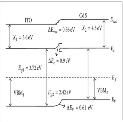
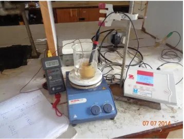
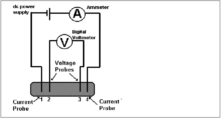
Electrical and Optical Characterization of Cu4SnS4 and CdS:B Thin Films For Photovoltaic Applications
Full text
Figure
Related documents
H9: When modeled with the structure of the labor market and relative power of labor, the quantity of job opportunities and quality of job opportunities are not related to
Figure 3(i) shows the output of proposed work which removes noise better by using combination of filters (notch filter and low pass filter) selected by fuzzy logic.
This smoothed structure is superimposed over the original text, producing the expandable outline shown in the left pane of Figure 2.. Paragraphs are along the
contains the SOlC address for which the line attachment as a secondary station will monitor in receive mode when a 'read' command has been given... The
To address the challenges described above, this paper proposes a dual-space model which incorporates external knowledge to enhance the semantic space produced by the
Thirty-six plant samples were placed into categories based on a visual assessment of Ephelis japonica hyphae (signs or no signs) combined with the experimental result of the
Learning and Memory in the Visual, Auditory, and Olfactory Modalities: An Investigation of the Generality of Serial Position Effects.. (Under the direction of James
Gyro bias estimate and error versus time with original filter parameters.. To reduce the influence of the terrain on the estimated states of
