• No results found

Electrical and Optical Characterization of Cu4SnS4 and CdS:B Thin Films For Photovoltaic Applications

N/A
N/A
Protected

Academic year: 2020

Share "Electrical and Optical Characterization of Cu4SnS4 and CdS:B Thin Films For Photovoltaic Applications"

Copied!
79
0
0

Loading.... (view fulltext now)

Full text

Figure

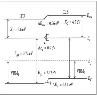
Figure 3.1: Energy band diagram of the ITO/CdS isotype heterojunction (Jain et al., 2006)
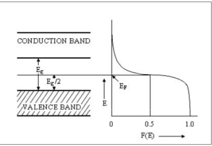
Figure 3.2: Intrinsic semiconductor Fermi level (Abdullah, 2007).
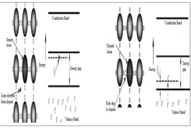
Figure 3.3: (a) n-type semiconductor and p–type semiconductor. (Silva, 2010)
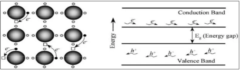
Figure 3.3: (c) Interactions of energy in (a) window, (b) absorber materials (Abdullah, 2007)
+7

References

Related documents