Novel Compact and Dual-Broadband Microstrip MIMO Antennas
for Wireless Applications
Hussein Hamed Mahmoud Ghouz*
Abstract—Two novel microstrip MIMO antennas have been proposed and presented in this paper. The objective is to design a compact and dual-broadband MIMO antenna module appropriate for many wireless devices including WLAN, LTE and WiMax. The presented MIMO antennas have been analyzed, designed, simulated and investigated using CST MW simulator. They have been fabricated (FR-4 substrate), and their scattering matrices and total efficiencies have been measured. The first MIMO antenna module is composed of four proposed broadband microstrip antennas arranged in two MIMO antenna pairs. The first MIMO pair resonates at 5.2 GHz (5.08–5.313 GHz) while the second pair resonates at 5.8 GHz (5.643–5.96 GHz). This MIMO antenna has a compact size of 40×40 mm2, dual-broadband, minimum mutual coupling below −25 dB, bandwidth greater than 225 MHz and gain of 3.8 dBi. The second MIMO antenna module consists of two proposed and modified dual-broadband microstrip monopole antennas, where, each has a dual resonance at 3.7 GHz (3.46–3.94 GHz) and 5.2 GHz (4.99–5.41 GHz). This MIMO antenna has an overall compact size of 20×50 mm2, minimum coupling below −22 dB, bandwidth greater than 425 MHz and gain of 2.5 dBi. Good agreement has been achieved between measured and simulated results. The proposed MIMO antennas cover many wireless applications with the following specifications: compact size, dual-broadband, moderate gain, good efficiency and high port-to-port isolation.
1. INTRODUCTION
In the last decade, Multiple-Input-Multiple-Output (MIMO) technique has been widely used in wireless mobile and communication systems, in particular, 3G and 4G portable devices, to increase channel capacity, provide high data rate, and improve signal quality in fading environment [1–5]. This technique uses multiple antennas mounted on a single motherboard at both transmitter and receiver, and they operate in the same frequency band(s). However, such a technique adds additional challenges to the antenna design where; the required MIMO specifications should be achieved, including overall MIMO antenna size (practical constrain) and the mutual couplings between individual antennas on one PCB (signal quality design constrain). These constrains should be achieved simultaneously to design a good MIMO antenna. Lots of researches have been done to design a MIMO antenna having the required size and minimum coupling for a specific application, including many approaches to minimize the coupling under size constrain. In 2010, Zhou et al. proposed MIMO antenna array for mobile handset operating in the band (1.6–2.6) GHz with−11 dB coupling [6]. In 2011, a novel multiband antenna was proposed and reported with dual-broadband (0.8–1.2 & 1.6–2.7) GHz [7]. This antenna can be used for MIMO design and has wide range of applications including wireless mobile and sensors devices. A broadband microstrip MIMO antenna having multi-slots (two orthogonal E-shape patch antennas) was used for WiMax applications (5.2–6) GHz, and it was reported in [8]. In April 2012, See et al. proposed
Received 13 May 2015, Accepted 8 July 2015, Scheduled 16 July 2015
* Corresponding author: Hussein Hamed Mahmoud Ghouz (hussein.ghouz@aast.edu).
a wideband printed monopole MIMO antenna for WiFi and WiMax applications (2.2–4.2) GHz [9]. Another wideband MIMO antenna was proposed and reported for WiMax and 4G applications (2.4– 6.55) GHz [10]. Two-monopole-antenna system decoupled by using the neutralization-line technique was proposed and reported for wireless module card-solution in the band (2.2–2.5) GHz [11]. Also, a high gain (3.5 dBi), high isolation (−15 dB) and compact MIMO slot array antenna (55×95 mm2) for handheld devices (2–3) GHz was proposed in 2012 by Ayatollahi et al. and reported in [12]. Defective ground structure (DGS) concept was used to provide high isolation (−22.5 dB) over a wideband for mobile handset MIMO antenna (0.5–3) GHz [13]. In 2013, other microstrip MIMO antennas covering LTE mobile (0.7–0.85) GHz and mobile terminals (2.2–6.5) GHz were reported in [14–16]. Recently, many MIMO antennas for WiFi<E (1.7–3.8) GHz, WLAN (2–8) GHz, WiMax (4.8–6.5) GHz and handheld devices (0.7–0.9) GHz applications were proposed and reported in [17–23]. In 2015, Li et al. proposed and analyzed a wideband indoor WLAN/WiMax MIMO base station array (5.2/5.5/5.8 GHz) consisting of sixteen elements of folded dipoles excited by an E-shaped microstrip feed line [24]. Adual band microstrip antenna (2.37–2.48 GHz) and (3.46–3.56 GHz) was proposed and reported by Kadu et al. for ISM and WiMax MIMO system [25]. Other publications include design and analysis of microstrip antenna using modified slotted ground plane for mobile phone handsets [26–28]. Slotted ground plane was used either to control the antenna resonance frequency(s) or to reduce the mutual coupling between MIMO antenna ports. In fact, to design a good MIMO antenna, isolation, overall MIMO size and MIMO antenna parameters (pattern, gain, efficiency, bandwidth, VSWR, and polarization) should be taken into account simultaneously. Such a task represents the actual challenge facing the antenna designers. In this paper, two novel compact and dual-broadband microstrip MIMO antennas are designed, analyzed, investigated, fabricated, and measured. The proposed MIMO antennas resonate within the 3G/4G band and have a wide range of applications in wireless communication systems. Section 2 presents a detailed description of the two proposed microstrip patch antennas. The proposed microstrip MIMO antennas are fully described and presented in Section 3. Simulation results are presented and discussed in Section 4. A detailed parametric study of the key antenna dimensions is also presented in this section. The fabricated MIMO antennas are presented and discussed in Section 5. Finally, the paper is concluded in the last section.
2. PROPOSED MICROSTRIP ANTENNAS: DESIGN AND DESCRIPTION
A conventional microstrip square patch antenna (CP) with transmission line feed (Lf & Wf) of
50 Ohm is presented in Fig. 1. This patch is mounted on an FR-4 substrate (εr = 4.7, tangent loss
δ= 0.025, conductor thickness t= 0.035 mm and height h= 1.6 mm). Patch and substrate dimensions (Lp =Wp = 10.0 mm & Ls =Ws = 20.0 mm) were chosen to be compact in size, and then, the patch shape is reconfigured as well as the ground plane to tune the patch for the desired frequency band. Starting with the CP antenna, two microstrip patch antenna types have been proposed and presented in Fig. 2. The first patch antenna is a conventional square patch (full ground) having edge slots and feed line side slots (deep inset) as shown in Fig. 2(a). The patch edge slots are identical and symmetric
(a) Without Inset (b) With Inset
side slots (Left/Right) and upper patch slot (single centered edge slot). The dimensions of these slots (edges and inset) have been investigated and optimized for a specific application (WiMax). The second proposed microstrip antenna, a modified monopole antenna, is shown in Fig. 2(b). The ground plane is a defective ground structure (DGS) having a rectangular window under patch and four slots under feeder as shown in Fig. 2(c) and Fig. 2(d). The patch resonator has the same shape and dimensions as the first proposed patch antenna. This adds a new set of key parameters to control and tune the antenna resonance frequency(s). Dimensions of the conventional microstrip antenna and proposed microstrip antennas are listed in Table 1 (The symbols are indicated in Fig. 1 and Fig. 2).
(a) Top view (b) Top view (c) Bottom view (DGS) (d) Zoom view of slots under feeder
Figure 2. Proposed dual broadband microstrip antennas (DBBMS): (a) Top view (x-y plane) of DBBMS antenna with full ground plane (no slots). (b), (c) Different views (x-yplane) DBBMS antenna with DGS plane, and (d) Zoom view.
Table 1. Dimensions (in mm) of square patch, edge slots, feed slots (inset) and ground slots (DGS).
Parameters Le11 Le12 W e11 W e12 Le2 W e2 Lp Wp
Values 5 5 1.25 1.25 1 4 10 10
Parameters Ws Ls L1 L2 Lf Wf W1 L11
Values 20 20 4 4 6.75 3.2 5 6.5
Parameters L12 L13 L14 L15 L16 L17 S W12
Values 13.5 12.5 6.75 4 4.75 5.25 0.25 18
Parameters W13 W14 W15 Y X
Values 14 8 15 2.5 4.5 7.5 0.7
3. PROPOSED MICROSTRIP MIMO ANTENNAS: DESCRIPTION AND DESIGN
(a) (b)
Figure 3. First proposed dual broadband microstrip MIMO antenna (all views are in x-y plane). (a) MIMO I top view. (b) MIMO I bottom view (DGS).
(a) (b)
(c) (d) (e)
Figure 4. Second proposed dual broadband monopole MIMO antenna (MIMO II) (all views are inx-y plane). (a) MIMO II top view. (b) Bottom view of IGS. (c) Bottom view of FCGS. (d) Bottom view of PCGS. (e) PCGS Zoom.
Table 2. Dimension (in mm) of MIMO I, MIMO II and DGS.
Parameters Lsub Wsub d1 d2 d3 d4
Values 40 40 10.25 9.25 10.5 10.25
Parameters D1 D2 L4 L5 L6 L7 L8 L9
Values 27 29.9 23 17 19.5 16 5 17
Parameters W2 W3 W4 W5 W6 W7 W8 S
Values 17 30 5 17 19.5 15 15.5 1
Parameters Lsub1 Wsub1 Wm Ws1 Ws2 Ls1 X Y
grounds (FCGS) and partially connected grounds (PCGS) as shown in Fig. 4(b) through Fig. 4(d), respectively. The dimensions of the proposed MIMO antennas (The symbols are illustrated in the presented figures) are presented in Table 2.
4. SIMULATION RESULTS AND DISCUSSION 4.1. Proposed Microstrip Antennas
In this section, the microstrip patch antennas, presented in the previous sections, have been analyzed, simulated and investigated using the CST-MW simulator. First, the resonance frequency of the conventional square patch antenna (CP) has been investigated for different lengths of feeder side slots (Y inset). The assumed dimensions for the presented simulation were illustrated in Table 1. Simulation results are shown in Fig. 5(a). As it is clear from figure, the patch resonance frequency is very sensitive to the feeder side slots compared to conventional patch (without inset). This is due to the variation of the patch input impedance at the feeding point location as compared to the characteristic impedance (50 Ω) of the feed line. Therefore, the feeder side slots can be used to control the patch resonance
(a)
(b)
(c)
Figure 5. |S11| of the proposed microstrip square patch antennas. (a) |S11| of the microstrip patch
for different feeder side slots as compared to the conventional patch. (b) |S11| of the first proposed
microstrip patch antenna for feeder side slots and patch edge slots. (c) |S11| of the second proposed
frequency in a coarse manner (from 13.65 GHz to 5.8 GHz). Second, simulated return losses “|S11|”
of the two proposed microstrip antennas are presented in Fig. 5(b) and Fig. 5(c), respectively. In the case of the first proposed microstrip antenna, it is clear that the patch side edge slots can be used to finely adjust its resonance frequency as shown in Fig. 5(b) (from 6.8 GHz for X = 4.0 to 6.5 GHz for X = 4.0 plus patch side edge slots). On the other hand, the presence of ground slots (DGS) adds other key parameters to control the patch resonance frequency as clear from Fig. 5(c). In this case, the effect of the proposed DGS creates another resonance at3.7GHz beside a shifted resonance at5.2GHz instead of 5.5GHz. Thus, this proposed antenna is a modified dual-broadband monopole antenna for LTE/WiMax applications. Furthermore, to fully understand the impact of feeder side slots,patch side edge slots and ground slots (DGS) on the resonance frequency of the proposed microstrip antennas, the surface current densities distribution on the patch and the ground have been evaluated and compared to the case of conventional square patch “CP” (no patch slots, no feeder and ground slots).
Simulation results of current densities are illustrated in Fig. 6 with the indicated frequencies. It is clear from the presented figure that different current distributions have been obtained for each feeder side slots value as compared to the CP case (Fig. 6(a) through Fig. 6(d)). This current variation (impedance) lead to different equivalent electric patch lengths where, the patch resonates differently for each corresponding electric length. On the other hand, patch side edge slots adds a moderate current variation as compared to the feeder side slots (see Fig. 6(e) and Fig. 6(f)), which lead to additional
(a) 13.65 (b) 10.95 (c) 6.8 (d) 5.80 (e) 6.5 (f) 5.45
(g) 3.7 (h) 5.158
Figure 6. Surface current density of the proposed microstrip antennas at the indicated frequencies (GHz): (a)–(d) CP, (e) and (f) first proposed microstrip patch antenna, and (g) and (h) second proposed microstrip patch antenna.
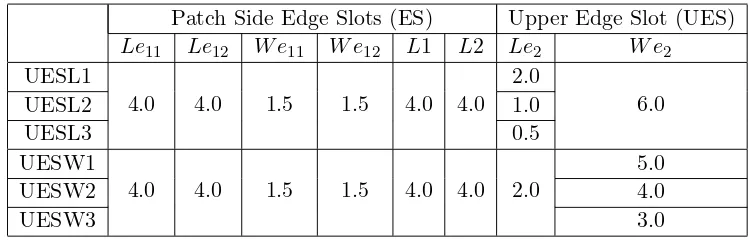
Table 3. Dimensions of the patch Upper Edge Slot (UES: X= 0.7 mm and Y = 7.5 mm).
Patch Side Edge Slots (ES) Upper Edge Slot (UES) Le11 Le12 W e11 W e12 L1 L2 Le2 W e2
UESL1
4.0 4.0 1.5 1.5 4.0 4.0
2.0
6.0
UESL2 1.0
UESL3 0.5
UESW1
4.0 4.0 1.5 1.5 4.0 4.0 2.0
5.0
UESW2 4.0
frequency control. Moreover, the presence of ground slots (DGS) does not alter the patch current distribution; however, the surface current is more concentrated on the feeder part where the ground slots are located below it. In addition, the surface current on ground plane has been totally altered due to the presence of the rectangular slots under the patch and feeder. In this case, the proposed microstrip antenna (presented in Fig. 2(c)) has two equivalent electric current sources; the patch current and DGS current resonate at dual-frequencies. The patch and ground current distribution of the dual frequencies are presented in Fig. 6(g) and Fig. 6(h), respectively (3.7 and 5.148 GHz). Therefore, resonance frequencies of the proposed microstrip antennas can be tuned to specific application using the feeder side slots, the patch edge slots and the ground slots (DGS).
Based on the above discussion of the obtained results, a full parametric study to investigate the effects of patch side edge slots on the antenna resonance has been carried out (length and width of the patch upper edge slot and side edge slots). In this case, the dimensions of the feeder side slots are assumed constant, where, dimensions of the patch side edge slots are optimized versus the patch
Table 4. Dimensions of the patch side Edge Slots ((Left/Right): LES/RES: X = 0.7 mm and Y = 7.5 mm).
Patch Side Edge Slots (ES) Upper Edge Slot (UES) Le11 Le12 W e11 W e12 L1 L2 Le2 W e2
LESL1/W1 4.0
4.0
1.5 1.5 4.0 4.0 1.0 6.0
LESL2 3.0
LESL3 2.0
LESW2
4.0 1.0 1.5 4.0 4.0 1.0 6.0
LESW3 0.5
(a)
(b)
Figure 7. |S11|of the first proposed antenna for different patch upper edge slot dimensions and constant
patch side edge slots and feeder side slots. (a) |S11| of our different lengths of the patch upper edge
slot (UESL1 to UESL3: X = 0.7 mm & Y = 7.5 mm). (b) |S11|of four different widths of the patch
resonance frequency. The variation of the patch side and upper edge slots are indicated in Table 3 and Table 4, respectively. The parameter values listed in these tables are organized as follows. The first column (at left) of Table 3 represents the “Length/Width” symbol of the patch upper edge slot (UESLi/UESWi,i= 1, 2, 3), where, the dimensions of patch side edge slots (Left/Right) are assumed constant (2nd column through 7th column). Similarly, symbols of the patch side edge slots are located in the first column (at left) of Table 4 (LESLi/LESWi, i= 1, 2, 3), where, dimensions of the patch upper edge slot are assumed constant. Simulation results of this parametric study are presented in Fig. 7 and Fig. 8. The resonance frequency is shifted down as the upper edge slot length and/or width decreases (see Fig. 7). However, the bandwidth of each resonance is almost the same. Similar results have been obtained in the case of patch side edge slots as shown in Fig. 8. Therefore, the patch side
(a)
(b)
Figure 8. |S11|of the first proposed antenna for different patch side edge slots dimensions (left edge)
and constant patch upper edge slot and feeder side slots. (a)|S11|for different lengths of the patch left
edge slots (LESL1 to LESL3: X = 0.7 mm &Y = 7.5 mm). (b)|S11|for different widths of the patch
left edge slots (LESW1 to LESW3: X= 0.7 mm & Y = 7.5 mm).
Table 5. Optimized dimensions of the proposed MS antennas (X= 0.7 mm, and Y = 4.0 mm and/or 7.5 mm).
Antenna Type SES UES Antenna Shape
Le11 Le12 W e11 W e12 L1 L2 Le2 W e2
Inset 7.5 Edge S1: Type 1 4.5 4.5 1.5 1.5 4 4 0.5 3 Fig. 2(a) with different insets and patch edge slots Inset 4.0 Edge S2: Type 2 4.5 4.5 1.25 0.75 4 4 1 3
CP Inset 4.0: Type 3
Patch with different insets only (No edge Slots) Fig. 1(b) CP Inset 7.5: Type 4
edge slots (left/right/upper) act as adjustable parameters built in resonance circuit to control the patch resonance frequency(s).
A similar detailed parametric study of the DGS slots dimensions (length and width) has been done to optimize and tune the dual resonance frequencies of the second proposed microstrip monopole antenna. Only the optimized return loss is presented in this paper. The final optimized dimensions of the five proposed microstrip patch antennas are listed in Table 5. The main parameters of the proposed antennas have been computed, and they are summarized and listed in Table 6. The optimized return losses of the proposed antennas are depicted in Fig. 9. It is clear from this figure that all the proposed microstrip antennas are single frequency broadband antennas (Type 1 to Type 4), and only one antenna is dual-broadband in the frequency range of interest (Type 5). In fact, the proposed antenna Type 5 has dual applications (LTE/WiMax indoor/outdoor devices). The other proposed antennas cover several applications including WLAN and WiMax. In addition, the radiation patterns inE-H planes (y-z and x-z planes) of the proposed antennas are computed and presented in Fig. 10. The first four proposed antennas have a directive pattern with a moderate side lobe level, wide beamwidth, linear polarization, and maximum directed toward nonzero angle (Θ = 0◦). On the other hand, the proposed antenna Type 5 has an omnidirectional pattern, and thus it is dual-broadband monopole antenna having linear polarization.
Table 6. Parameters of the five proposed MS antennas (Fo in GHz and BW1 (−10 dB) in MHz). Proposed Antennas Fo Go (dBi) Eff (%) BW1 VSWR
Inset 7.5 Edge S1: Type 1 5.186 3.20 60.70 245 1.126–2.0 Inset 4.0 Edge S2: Type 2 6.5 1.87 42.30 220 1.22–2.0
MS CP Inset 4: Type 3 6.824 2.63 47.00 265 1.046–2.0 MS CP Inset 7.5: Type 4 5.8 3.68 65.33 300 1.14–2.0
Inset 7.5 Edge S1 DGS: Type 5 3.7 2.6 85.00 500 1.09–2.0
5.158 3.00 70.00 420 1.12–2.0
Figure 9. |S11| of the proposed microstrip patch antennas (from Type 1 to Type 5).
Type_1 Type_2 Type_3 Type_4 Type_5
4.2. Proposed Microstrip MIMO Antennas
Three proposed microstrip patch antennas have been selected for MIMO antenna design. These are antenna Type 1, Type 4 and Type 5 which are presented and discussed in the previous section. The specifications of these proposed antennas were computed previously, and their applications were discussed. Two MIMO antennas have been proposed, designed and investigated. The MIMO design problem is how to achieve minimum mutual coupling between the adjacent ports of the multiple antennas. In this work, mutual coupling has been minimized using DGS concept along with orthogonal orientation of the multiple antennas in the case of the first proposed MIMO antenna (MIMO I, see Fig. 3(b)). On the other hand, the grounds of the two adjacent antennas are partially connected (PCGS) with extended spacing between them to minimize the overall mutual coupling dependent on the individual antennas orientation. This proposed approach (PCGS) has been used for the second MIMO antenna to minimize the mutual coupling (MIMO II, see Fig. 4(d)). Return loss and radiation pattern of MIMO I antenna have been computed and presented in Fig. 11 and Fig. 12, respectively. The proposed DGS achieves minimum mutual coupling (below−25 dB) and does not alter the antenna specifications of the single antenna, including resonance frequency, gain, and radiation pattern (see Fig. 12). The main MIMO antenna parameters have been computed and summarized in Table 7. Thus, the proposed MIMO I antenna is a compact and dual-broadband MIMO antenna having overall size 40×40 mm2, and it can be used for WLAN and WiMax application devices.
Figure 11. |S11|of the first proposed microstrip MIMO I antenna.
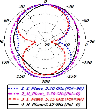
Figure 12. Radiation pattern of the proposed MIMO I antenna at its resonance frequencies inE-plane and H-plane.
Table 7. Parameters of the first proposed MIMO antenna (Fo in GHz and BW in MHz).
MIMO I
Fo Go dBi Eff % BW1 (−10 dB) BW2 (−6 dB) VSWR Coupling
5.2 3.80 58 227 390 1.13–2.0
Below −25 dB
Figure 13. |S11|of the second proposed MIMO II antenna for two different ground geometries.
Figure 14. |S11|of the second proposed MIMO II antenna with PCGS as compared to the proposed
antenna Type 5.
Figure 15. Radiation pattern microstrip MIMO II antenna at its resonance frequencies in E-plane and H-plane.
Table 8. Parameters of the second proposed MIMO II antenna (Fo in GHz and BW in MHz).
Fo Go (dBi) Eff % BW1 (−10 dB) BW2 (−6 dB) VSWR Coup. (dB)
IGS (B1) 3.62 2.8 83 540 920 1.071–2.0 −12
5.16 2.8 66 380 715 1.18–2.0 −18
FCGS (B2) 3.94 1.9 68 300 530 1.2–2.0 −19
5.16 2.9 77 410 765 1.2–2.0 −22
PCGS (B3) 3.75 2.5 84 480 790 1.09–2.0 −22
5.15 3.00 70 420 810 1.06–2.0 −20
5. FABRICATIONS AND MEASUREMENTS
The proposed MIMO antenna modules (MIMO I & MIMO II) have been fabricated on an FR-4 substrate, and their parameters (scattering matrices and total efficiencies) have been measured and compared to the simulated results as presented in Fig. 16 and Fig. 17, respectively. It is clear from
(a) (b)
(c) (d)
(a) (b)
Figure 17. Simulated and Measured total efficiencies of the proposed MIMO antennas: (a) MIMO I, (b) MIMO II.
Fig. 16 that good agreement has been achieved between measured and simulated results for the first MIMO antenna including return losses and mutual coupling (see Fig. 16(a) and Fig. 16(b)). However, small deviations between the measured and simulated return losses with reasonable agreement have been noticed in case of second MIMO antenna (see Fig. 16(c)). In fact, this is due to fabrication error and soldering points of SMA connectors. Moreover, good agreement has been achieved between measured and simulated total efficiencies of each MIMO antenna configuration as presented in Fig. 17.
6. CONCLUSION
Two novel designs of compact and dual-broadband MIMO antennas have been proposed and presented. The single MIMO element is a microstrip antenna type with transmission line feed. Three microstrip antenna types have been proposed, designed and selected to construct the MIMO antennas. The first antenna type is a microstrip square patch having deep inset and full ground plane. Patch side edge slots (left/right/upper) with different lengths and widths have been added to the patch of the first antenna to construct the second antenna type. The third antenna type has the same patch as the second antenna, but it has defective ground plane instead of full ground. This ground has one rectangular slot under patch and four slots under feeder. A detailed parametric study has been conducted using CST MW studio to optimize the parameters as well as dimensions of the proposed microstrip antennas and MIMO antennas. In addition, MIMO antennas have been fabricated on an FR-4 substrate, and their parameters have been measured. Simulation results show that good MIMO antenna parameters have been achieved, including high port-to-port isolations (22–27 dB), gains (2.5–4.9 dBi), bandwidths (225– 480 MHz), efficiencies (58–84%), VSWR (1.06–2.0) and compact size module (40×40 mm2–20×50 mm2). The measured return losses, total efficiencies and coupling between ports are in a reasonable agreement with the simulated results. The proposed MIMO antennas have many wireless applications including LTE (3.4–4.0 GHz) and WLAN/WiMax ([5.0–5.3] and [5.6–6.0] GHz) with high port-to-port isolation. Finally, a compact array size composed of four MIMO antenna modules (MIMO I and/or MIMO II) can be designed to achieve high gain (10–12 dBi) for standard indoor/outdoorLTE/WiMax devices.
REFERENCES
1. Vaughnan, R. G. and J. B. Andersen, “Antenna diversity in mobile communication,” IEEE Transactions on Vehicular Technology, Vol. 36, No. 4, 149–172, 1987.
2. Foschini, G. J. and M. J. Gans, “On limits of wireless communications in a fading environment when using multiple antennas,”Wireless Personal Communication, Vol. 6, 311–335, 1998.
communication,” 50th Proc. IEEE Vehicular Technology Conference, Vol. 1, 381–385, Amsterdam, Netherlands, Sep. 1999.
4. Shin, H. and J. H. Lee, “Capacity of multiple-antenna fading channels: Spatial fading correlation, double scattering, and keyhole,”IEEE Transactions on Information Theory, Vol. 49, No. 10, 2636– 2647, Oct. 2003.
5. Kumaravel, K., “Comparative study of 3G and 4G in mobile technology,” IJCSI International Journal of Computer Science Issues, Vol. 8, No. 5(3), 256–263, Sep. 2011.
6. Zhou, X., R. Li, and M. M. Tentzeris, “A compact broadband MIMO antenna for mobile handset applications,” International Symposium (APSURSI) on Antennas and Propagation, 1–4, 2010. 7. Zhang, T., et al., “A novel multiband planar antenna for GSM/UMTS/LTE/Zigbee/RFID mobile
devices,”IEEE Transactions on Antennas and Propagation, Vol. 59, No. 11, 4209–4214, Nov. 2011. 8. Jagadeesh Babu, K., K. Sri Rama Krishna, and L. Pratap Reddy, “A multi slot patch antenna for 4G MIMO communications,” International Journal of Future Generation Communication and Networking, Vol. 4, No. 2, 105–112, Jun. 2011.
9. See, C. H., et al., “Wideband printed MIMO/diversity monopole antenna for WiFi/WiMax applications,” IEEE Transactions on Antennas and Propagation, Vol. 60, No. 4, 2028–2035, Apr. 2012.
10. Li, J.-F., Q.-X. Chu, and T.-G. Huang, “A compact wideband MIMO antenna with two novel bent slits,”IEEE Transactions on Antennas and Propagation, Vol. 60, No. 2, 482–489, Feb. 2012. 11. Su, S.-W., C.-T. Lee, and F.-S. Chang, “Printed MIMO-antenna system using neutralization-line
technique for wireless USB-dongle applications,”IEEE Transactions on Antennas and Propagation, Vol. 60, No. 2, 456–463, Feb. 2012.
12. Ayatollahi, M., Q. Rao, and D. Wang, “A compact, high isolation and wide bandwidth antenna array for long term evolution wireless devices,”IEEE Transactions on Antennas and Propagation, Vol. 60, No. 10, 4960–4963, Oct. 2012.
13. Lee, S. H., C. Y. Yang, and W. G. Yang, “High isolation MIMO antenna design by using ground slits for mobile handset,”PIERS Proceedings, 589–593, Moscow, Russia, Aug. 19–23, 2012.
14. Zulkifli, F. Y., Daryanto, and E. T. Rahardjo, “Slot ring triangular patch antenna with stub for MIMO 2×2 wireless broadband applications,” Proceedings of the International Symposium on Antennas and Propagation (ISAP), Vol. 2, 885–887, 2013.
15. Zhao, X., Y. Lee, and J. Choi, “MIMO antenna using resonance of ground planes for LTE mobile application,”IEEE International Symposium (APSURSI) on Antennas and Propagation, 184–185, 2013.
16. Xia, X.-X., Q.-X. Chu, and J.-F. Li, “Design of a compact wideband MIMO antenna for mobile terminals,” Progress In Electromagnetics Research C, Vol. 41, 163–174, 2013.
17. Addaci, R., et al., “Dual-band WLAN multiantenna system and diversity/MIMO performance evaluation,” IEEE Transactions on Antennas and Propagation, Vol. 62, No. 3, 1409–1415, Mar. 2014.
18. Dioum, I., et al., “A novel compact dual-band LTE antenna-system for MIMO operation,” IEEE Transactions on Antennas and Propagation, Vol. 62, No. 4, 2291–2296, Apr. 2014.
19. Roshan, R. and R. K. Singh, “Dual ISM band MIMO antenna for WiFi and WiMax application,” International Conference on Signal Propagation and Computer Technology (ICSPCT), 209–213, 2014.
20. Yeh, J.-T., et al., “Compact internal antenna for handheld devices with comprehensive DTV band coverage,”IEEE Transactions on Antennas and Propagation, Vol. 62, No. 8, 3998–4007, Aug. 2014. 21. Wang, H., et al., “Wideband tri-port MIMO antenna with compact size and directional radiation
pattern,” Electronics Letters, Vol. 50, No. 18, 1261–1262, Aug. 28, 2014.
23. And´ujar, A. and J. Anguera, “MIMO multiband antenna system with non-resonant elements,” Microwave and Optical Technology Letters, Vol. 57, No. 1, 183–190, Jan. 2015.
24. Li, G., et al., “AMC-loaded wideband base station antenna for indoor access point in MIMO system,” IEEE Transactions on Antennas and Propagation, Vol. 63, No. 2, 525–533, Jan. 2015. 25. Kadu, M. B., et al., “Dual band microstrip patch antenna for MIMO system,” International
Conferenceon Pervasive Computing (ICPC), 1–4, Pune, Jan. 8–10, 2015.
26. Anguera, J., I. Sanz, J. Mumbr´u, and C. Puente, “Multi-band handset antenna with a parallel excitation of PIFA and slot radiators,” IEEE Transactions on Antennas and Propagation, Vol. 58, No. 2, 348–356, Feb. 2010.
27. Abedin, M. F. and M. Ali, “Modifying the ground plane and its effect on planar inverted-F antennas (PIFAs) for mobile phone handsets,” IEEE Antennas and Wireless Propagation Letters, Vol. 2, 2003.