Radiation Pattern Analysis and Modelling of Coplanar Vivaldi
Antenna Element for Linear Array Pattern Evaluation
Nurhayati1, 2, *, Eko Setijadi1, and Gamantyo Hendrantoro1
Abstract—This paper reports an electric field approximation model of the Coplanar Vivaldi antenna on the E-plane. The study is conducted in three stages, i.e., (i) evaluating the impact of various geometrical parameters to the Vivaldi’s element performance at different frequencies, (ii) modeling the electric field patterns, and (iii) applying the model to evaluate the linear total array pattern. The examination of the Coplanar Vivaldi element with fractional bandwidth of 133% in the 2–10 GHz band shows the individual roles of the antenna width, the tapered slot length, the opening width and the slope of the tapered slot in determining the VSWR, resistance, reactance and E-Field performance. The Vivaldi element should be designed with element width more than 0.5λ and less than λ to reach better performance of VSWR and E-field. The longer the tapered slot (> λ) with the high value of opening rate of tapered slot, the smaller the E-field. The E-field increases with increasing opening width of the tapered slot. Knowledge of the influence of each geometry parameter is then used as a reference in developing theE-field pattern approximation model of the Vivaldi element. The derivation of the Vivaldi approximation model is started from the pattern of a horn antenna because both antennas share a similar feature, i.e., the enclosure of theE-field propagation within a tapered slot resulting in a directional radiation pattern. The result of Coplanar Vivaldi modeling is verified against the results of electromagnetic computational simulation and measurement. The Vivaldi element model is useful for total array pattern analysis to save computation time and to provide flexibility in the evaluation of array design.
1. INTRODUCTION
Vivaldi antenna is a planar antenna with a light weight, low profile, wide bandwidth, directional radiation pattern, and high gain [1–4] Vivaldi antenna can be applied for through-wall detection [5], imaging [6], radar [7, 8] and communication [9]. Many studies on Vivaldi antenna have been aimed to improve the performance, using numerical electromagnetic computation for evaluation. Bandwidth and radiation pattern performance of Vivaldi antenna depends on the geometry such as the length and the width, the mouth opening of tapered slot and the slope of tapered slot. The feeding shape, the radiator shape and the substrate also predispose the bandwidth and radiation pattern performance.
In terms of the design structure, Vivaldi antennas can be divided into three classes, i.e., Coplanar Vivaldi Antenna, Antipodal Vivaldi Antenna (AVA) and Balanced Antipodal Vivaldi Antenna (BAVA), each with its own strengths. For instance, the family of AVA generally shows high gain and wide [10–12]. However, the wide bandwidth implies the emergence of grating lobes when the antennas are used in array configuration especially in high frequency region of the band [13]. Accordingly, in this paper, we focus on Coplanar Vivaldi antenna.
Parametric studies of several dimensions of Vivaldi antenna with respect to impedance and VSWR performance have been published in [14, 15]. However, while in a Vivaldi array the element pattern
Received 5 April 2019, Accepted 22 May 2019, Scheduled 14 June 2019 * Corresponding author: Nurhayati ([email protected]).
contributes the total array pattern [16, 17], parametric study of the Coplanar Vivaldi geometry with respect to the radiation pattern is still limited. Our first goal is to analyze the effect of geometry variation on VSWR, impedance and radiation pattern performance, that can be reference to design antenna element which will be discussed in Section 2.
Antenna array can enlarge gain, reduce beam width, and cover certain beam scanning [18]. On the other hand, arrays with uniform spacing suffer from mutual coupling [19], which for those with Coplanar Vivaldi elements can be mitigated by employing corrugated and/or truncated slot structures [13]. An example of large Vivaldi arrays are those with hundreds of elements that have been used in astronomy and telescope application. Array optimization, especially for those with a very large number of elements [20, 21], e.g., up to hundreds or thousands of them, requires very long computation time. It also requires a high-grade computer to analyze large Vivaldi array with electromagnetic numerical computation. In actual analysis, array optimization can be done by analytical methods so that the computation process can be made more flexible with signal processing techniques and, hence, faster. However, use of analytical method requires antenna element modelling.
Most analytical methods for array antenna have been reported by focusing on commonly used elements, such as isotropic [22], dipole [23], and microstrip [24]. Discussions of radiation pattern analysis of linear tapered slot antenna and slot line have been reported in [25, 26]. Nevertheless, the computational radiation pattern which is employed using the moment method by developing basis functions results in a more complex algorithm. For an antenna array, the total pattern can be obtained analytically by multiplying the E-field pattern of the element with the array factor. However, the mathematical expression for radiation pattern of a Vivaldi element is presently not available for use in Vivaldi array pattern analysis. Thus far, pattern analysis of a Vivaldi array must resort to computational electromagnetic algorithms. Therefore, it is necessary to develop analysis and modelling of the radiation pattern of a Vivaldi antenna which is related to its geometry and working frequency.
Horn and Vivaldi antennas have similarities in the presence of tapered structure and directional radiation pattern [27]. While horn is a volume antenna, Vivaldi antenna is planar. Both antennas have electric fields that propagate between the sides of the tapered structure.
The second objective of this paper is to develop a novel radiation pattern model of Vivaldi element using the same approach as used for horn antenna, to be discussed in Section 3. The use of such a mathematical model can reduce computation time and make analytical calculations more flexible. We evaluate the accuracy of the Coplanar Vivaldi element pattern model in Section 4 and the total array pattern obtained by pattern multiplication in Section 5 through comparison with results from CST simulation. Finally, Section 5 concludes this paper.
2. PARAMETER STUDY OF GEOMETRY
We start with the design of Vivaldi antenna element as shown in Fig. 1, in which FR4 substrate is used with permittivity of 4.6, substrate thickness of 1.6 mm, and copper thickness of 0.035 mm. It is designed
with slope of tapered slot as follows [13]:
y=C1eRx+C2, C1 = y2−y1
eRx2 −eRx1, C2 =
y1eRx2 −y2eRx1
eRx2 −eRx1 (1)
wherexandydenote coordinates in cartesian system;Ris the slope of the tapered; (x1, y1) and (x2, y2)
are the coordinates of the start and end of the tapered slot, respectively.
The Vivaldi antenna is designed to achieve a bandwidth of 133% based on VSWR (Voltage Standing Wave Ratio) of less than 2 in the 2–10 GHz range. The next step is to vary one of the antenna’s geometries and make the others fixed, without changing the shape of feed line and the type of substrate. The detailed design parameters of Coplanar Vivaldi Element as shown in Fig. 1 are listed in Table 1.
Table 1. Geometry of antenna element based on Figure 1.
Parameter Dimension (mm) Parameter Dimension (mm)
L 60 r 3
W 60 Wf 2.5
Wt 30 Df 3
Lt 42.5 xf 4
Lsl 7.5 yf 5
Wsl 0.5 R 0.15
2.1. Antenna Width
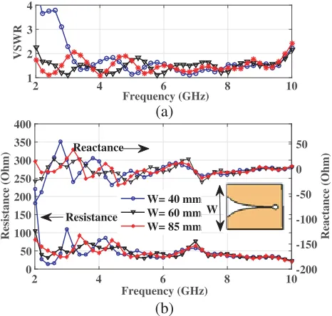
Figure 2(a) shows the variation in VSWR due to variation of antenna width (W) by settingL= 60 mm,
Wt = 30 mm, R = 0.15. Figure 2(a) shows VSWR for W = 40 mm, which at 2 GHz corresponds
to 0.267λ and results in VSWR > 2. It happens because the antenna is designed with W < 0.5λ
and indicates the occurrence of impedance mismatch between the radiator and free space so that the
2 4 6 8 10
Frequency (GHz) 1
2 3 4
VSWR
W=40 mm W=60 mm W=85 mm
2 4 6 8 10
Frequency (GHz) 0
50 100 150 200 250 300 350 400
Resistance (Ohm)
-200 -150 -100 -50 0 50
Reactance (Ohm)
W= 40 mm W= 60 mm W= 85 mm Reactance
W Resistance
(a)
(b)
Figure 2. Effect of element width to (a) VSWR, and (b) resistance and reactance performance withL= 60 mm, Wt= 30 mm, R= 0.15.
0 2 4 6 8 10
E-field (V/m)
W=40 mm W=60 mm W=85 mm
0 2 4 6 8 10
0 2 4 6 8 10
(a) (b) (c)
-180 -90 0 90 180 -180 -90 0 90 180 -180 -90 0 90 180 θ ( )o θ ( )o θ ( )o
maximum power transfer is not fulfilled. At 3 GHz, the element width of 40 mm corresponds to 0.4λ, 60 mm to 0.6λ and 80 mm to 0.8λ. The result shows that an element width of more than 0.5λ with respect to its operating frequency results in VSWR <2 and, therefore, can be considered in antenna design as a reference to achieve the desired VSWR performance at the lowest frequency. Figure 2(b) presents the performance of resistance (bottom curve) and reactance (upper curve) for varying element width. Vivaldi antennas with an element width less than half wavelength demonstrate high resistance at the low-end frequency as shown in the lower curve of Figure 2(b). It also shows the fluctuation of reactance as shown in the upper side of Figure 2(b).
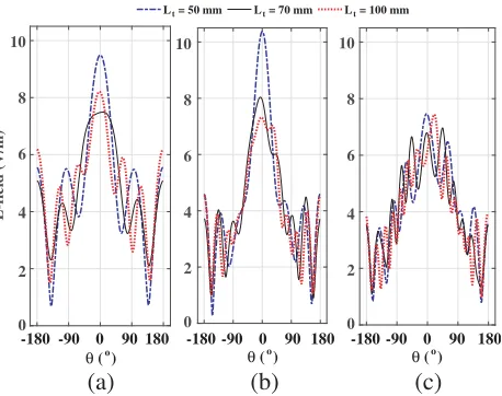
Figure 3 shows theE-field patterns obtained by changing the element width at frequencies of 3, 5, and 7 GHz. At 3 GHz (see Figure 3(a)), the Vivaldi antenna with element width of 40 mm or 0.4λ has the smallestE-field and VSWR>2. The size also produces high resistance and reactance and influences radiation pattern. Also at 3 GHz, the wider antennas yield higherE-fields for element width not more than 1λ. The figure also exhibits that the SLL performance ranges from best to worst forW = 80 mm, 60 mm and 40 mm, respectively. The E-field performance at 5 GHz (see Figure 3(b)) is reached from best to worst for W = 60 mm (1λ), W = 40 mm (0.667λ) and W = 80 mm (1.33λ), respectively. Meanwhile at 7 GHz, theE-field performance is obtained forW = 40 mm (0.93λ),W = 60 mm (1.4λa) and W = 80 mm (1.86λ), successively, from best to worst. An antenna with the element width of more than 0.5λbut less than 1λhas better E-field than others. Although an antenna has VSWR< 2, the
E-field at the high-end frequency depends on the width of antenna relative to its wavelength.
If the antenna element width is more than 1λ, it will yield a worse E-field than those with width less than 1λ. It can be seen in Figure 5 that at frequency 7 GHz, antenna width of 85 mm (1.85λ) yields more side lobes. Higher frequencies causes higher side lobe levels (SLL). From the description above it can be concluded that the antenna with element width less than 0.5λ will yield VSWR more than two, suffer from fluctuation of resistance and reactance, show a decrease inE-field and increase in the SLL (at low-end frequencies). Moreover, if an antenna is designed with element width more than 1λ, although it has VSWR less than 2, it degrades the E-field performance especially at the high-end frequency band, which causes high side lobe. Thus, it is necessary to design antenna by considering the element width relative to its desired operating frequency.
L = 50 mm L = 70 mm L = 100 mm
Frequency (GHz)
Lt = 50 mm
Lt = 70 mm
Lt = 100 mm Reactance
Resistance Lt
(a)
(b)
1 2 3 4
VSWR
0 50 100 150 200 250 300 350 400
Resistance (Ohm)
-200 -150 -100 -50 0 50
Reactance (Ohm)
2 4 6 8 10
Frequency (GHz)
2 3 4 5 6 7 8 9 10
Figure 4. Effect of of element length to (a) VSWR, resistance and reactance performance
W = 60 mm, Wt= 30 mm, R= 0.15.
Lt = 50 mm Lt = 70 mm Lt = 100 mm
0 2 4 6 8 10
E-field (V/m)
(a) (b) (c)
-180 -90 0 90 180 -180 -90 0 90 180 -180 -90 0 90 180
θ ( )o θ ( )o θ ( )o
0 2 4 6 8 10
0 2 4 6 8 10
2.2. Length of the Tapered Slot
VSWRs and impedance performances with various lengths of tapered slot (Lt) are shown in Figure 4,
taken for W = 60 mm,Wt= 30 mm,R= 0.15. The VSWR at the low-end frequency (2 GHz) descends
with the decreasing length, i.e., atLt = 100 mm (0.67λ), Lt= 70 mm (0.47λ) andLt= 50 mm (0.33λ) consecutively, reveals that longer size of tapered slot yields higher resistance, but the reactance alternates insignificantly. If the length of tapered slot is extended, but the opening rate is fixed, and the tapered slot opening mouth is small, it will increase VSWR. References [14, 15] explain that with smaller flare angle, which is related to the slope of the tapered slot, longer tapered slot yields higher resistance and reactance at the low-end frequency. However, we simulate elements with the same value ofR= 0.15 so that when the tapered slot is longer, VSWR becomes worse.
The effect of the length of tapered slot on the E field performance is depicted in Figure 5. At 3 GHz, a Vivaldi antenna with Lt = 50 mm (0.5λ) has higher E-field than that for Lt = 100 mm (1λ)
and 70 mm (0.7λ). It also shows that increasing E-field appears for the length of tapered slot (Lt) in
factor 0.5λ. It can be seen that tapered slot that has Lt= 0.5λand 1λhas better E-field compared to Lt= 0.7λ.
However, escalation ofLtwithR= 0.15 whileW remains small will yield worseE-field. At 5 GHz,
by setting Lt = 50 mm≈0.83λ, it yields an E-field higher than it does withLt = 70 mm≈1.16λ and Lt= 100 mm≈1.667λ. It shows that a longer tapered slot yields a smaller E-field. At 7 GHz, antennas
with Lt = 100 mm (2.33λ), Lt = 50 mm (1.17λ) and Lt = 70 mm (1.63λ) produce poor radiation
pattern. The longer the tapered slot (> 1λ) with the high value of R but small value of W yields a smaller E-field. A high value of R with a long tapered slot has a gradual slope in the beginning and the middle of the slot but with a drastic change at the end of tapered slot opening. This influences resonance at high frequency and yields high SLL, which is shown in Figure 5(c) and can be explained as follows. An antenna with a higher operating frequency has shorter wavelength than those at lower frequencies. For the same length of tapered slot (Lt) at high frequency, the antenna has more longer
tapered slot relative to its wavelength than at lower frequency.
1 2 3 4
VSWR
W
t=15 mm Wt=35 mm Wt=60 mm
0 50 100 150 200 250 300 350 400
Resistance (Ohm)
-200 -150 -100 -50 0 50
Reactance (Ohm)
Wt = 15 mm
Wt = 35 mm
Wt = 60 mm Wt
Reactance
Resistance
(a)
(b) Frequency (GHz)
2 4 6 8 10
Frequency (GHz)
2 4 6 8 10
Figure 6. Effect of opening mouth of tapered tapered slot to (a) VSWR and (b) resistance and reactanceLt= 50 mm,W = 60 mm andR = 0.15.
0 2 4 6 8 10 12
E-field (V/m)
W
t = 15 mm Wt = 35 mm Wt = 60 mm
0 2 4 6 8 10 12
0 2 4 6 8 10 12
(a) (b) (c)
-180 -90 0 90 180 -180 -90 0 90 180 -180 -90 0 90 180 θ ( )o θ ( )o θ ( )o
Figure 7. E-field on the E-plane with various opening mouth of tapered slot at frequency (a) 3 GHz, (b) 5 GHz and (c) 7 GHz Lt = 50 mm,
2.3. Opening Width of the Tapered Slot
The effects of the tapered slot opening size (Wt) on VSWR, resistance, and reactance performance
are presented in Figure 6 with Lt = 50 mm,W = 60 mm and R = 0.15. At 2 GHz, VSWR decreases
toward unity when the opening size is increased from Wt = 15 mm ≈ 0.1λ, Wt = 35 mm ≈ 0.23λ, to
Wt= 60 mm≈0.4λ. The literature [10, 11] explained that the smaller aperture height profits the wider low end of frequency, which is in contrast to our result that smaller opening of tapered slot increases the VSWR. That difference happens because our antenna is designed with high opening rate R. For resonance at the low-end frequency, the antenna should be designed with tapered slot opening of wider mouth, while antennas with small R can be designed with small Wt. Figure 7 shows that at 3 GHz
variation in Wt only slightly affects the resulting E-field, while at 5 GHz, a significant increase of E
Field is observed for Wt = 15 mm (0.25λ), Wt = 35 mm (0.583λ) and Wt = 60 mm (1λ) in ascending
order. At 7 GHz the same phenomenon happens for Wt = 15 mm (0.35λ), Wt = 35 mm (0.7λ) and Wt= 60 mm (1.4λ) in ascending order. Although the antenna exhibitsS11 below−10 dB at 2–10 GHz,
the performance ofE-field is diverse for different values ofWt. ForR= 0.15, andW = 60 mm, enlarged
tapered slot mouth opening yields an increase in E-fields.
2.4. Opening Rate of the Tapered Slot
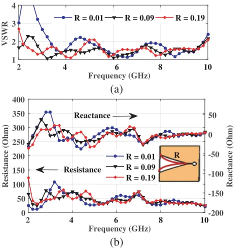
The effect of opening rate R on VSWR, resistance, and reactance can be seen in Figure 8 by setting
L = 60 mm, W = 60 mm, and Wt = 30 mm. Figure 8(a) shows that smaller R yields worse VSWR
for tapered slot length of 60 mm ≈0.6λ at 3 GHz, and Wt = 30 mm. Decreasing VSWR value at low
frequencies with the variation of R is obtained for R = 0.01, R = 0.09 and R = 0.19 respectively. At 2 GHz, increasing R, enlarges resistance as shown in the lower side of Figure 8(b). At 3 GHz, antenna with smallerR produces higher fluctuation of reactance than those with largerR as shown in the upper side of Figure 8(b).
The effect of modification of R on the performance of E-field at several frequencies is shown in
1 2 3 4
VSWR
R = 0.01 R = 0.09 R = 0.19
0 50 100 150 200 250 300 350 400
Resistance (Ohm)
-200 -150 -100 -50 0 50
Reactance (Ohm)
R = 0.01 R = 0.09 R = 0.19 Reactance
Resistance
R
(a)
(b)
Frequency (GHz)
2 4 6 8 10
Frequency (GHz)
2 4 6 8 10
Figure 8. Effect of opening rate R of tapered slot (a) VSWR and (b) resistance and reactance withLt= 50 mm, W = 60 mm and Wt= 30 mm.
0 2 4 6 8 10
E-field (V/m)
R = 0.001 R = 0.009 R = 0.19
0 2 4 6 8 10 12
0 2 4 6 8 10 12
(a) (b) (c)
-180 -90 0 90 180 -180 -90 0 90 180 -180 -90 0 90 180
θ ( )o θ ( )o
θ ( )o
Figure 9. E-field on the E-plane with various opening rateRat frequency (a) 3 GHz, (b) 5 GHz and (c) 7 GHz withLt= 50 mm,W = 60 mm and
Figure 9. At 3 GHz, the performances of E field are obtained for R = 0.01, R = 0.19 and R = 0.09, in ascending order. At 5 GHz, the antennas with R = 0.09 and R = 0.01 have similar E fields while the one with R = 0.19 results in the lowestE field. At 7 GHz the E-field performance is achieved for
R= 0.19,R= 0.09 andR = 0.001, in the ascending order. At lower frequency, variation in the opening rate of the tapered slot yields different characteristics of the main lobe, side lobe and back lobe. At high frequency, increasingR yields decreasingE field performance.
2.5. Variation of Geometry to the E-Field Performance
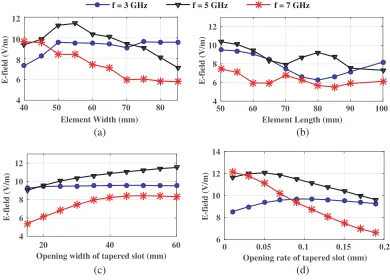
Figure 10 depicts the effect of changes in geometry on the maximum E-field performance at frequency 3, 5 and 7 GHz. Figure 10(a) shows the maximum E-field performance with various element width by setting L = 60 mm, Wt = 30 mm and R = 0.15. It shows that the increase of element width yields
escalation ofE Field performance at 3 GHz. On the other hand, at 5 GHz,E-field increases and peaks at aroundW = 55 mm≈0.92λ(5 GHz), and then declines. At 7 GHz, E Field tends to decrease with increasing antenna width because it has element width of more than 1λ.
40 50 60 70 80
Element Width (mm) 4
6 8 10 12
E-field (V/m)
f = 3 GHz f = 5 GHz f = 7 GHz
50 60 70 80 90 100
Element Length (mm) 4
6 8 10 12
20 40 60
Opening width of tapered slot (mm) 4
6 8 10 12
E-field (V/m)
0 0.05 0.1 0.15 0.2
Opening rate of tapered slot (mm) 6
8 10 12 14
(a) (b)
(c) (d)
E-field (V/m)
E-field (V/m)
Figure 10. E-field performance on the E-plane with variation: (a) The width of element, (b) the length of tapered slot, (c) the opening width of tapered slot and (d) the opening rate.
Figure 10(b) reveals the impact of varying tapered slot length (Lt) to the E field at W = 60 mm, Wt= 30 mm andR= 0.15. It can be observed that theEfield varies unequally at different frequencies.
At 3 GHz, withLt>50 mm (0.5λ) the element experiences decreasingE field until Lt= 80 mm (0.8λ),
after which it goes up. At 5 GHz, the E field decreases down to Lt = 70 mm (1.16λ), goes up again and peaks at Lt = 80 mm (1.33λ) then decreases again. At 7 GHz, variations of Lt with W = 60 mm,
Wt varying from 15 mm to 60 mm at 3 GHz. At 5 GHz and 7 GHz, E-field increases with increasing width of the tapered slot by setting L = 60 mm, W = 60 mm and R = 0.15. The high value of R
in small mouth opening Wt of the tapered slot causes the slope from the beginning of the slot to the
middle to change only a little. Furthermore, the slope will change drastically at the opening end of the tapered slot. It affects theE-fields at high frequency. Figure 10(d) represents the effect of the slope of tapered slot to E-field performance by setting L = 60 mm, W = 60 mm and Wt = 30 mm. At 3 GHz,
the greater R value, the greater the E field up to R = 0.1 after which the E-field comes down slowly. However, at 5 GHz and 7 GHz the greater R, the smaller E field. By setting Wt with fixed value, the
greater R yields the smaller flare angle and throat in the beginning of the slot, and it governs E-field performance at high frequency.
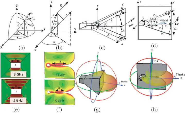
3. ANTENNA PATTERN MODELLING
Results of study on Vivaldi antenna geometry and performance in Section 2 indicate that the radiation pattern depends on the antenna geometry parameters. In this section, we use the derivation of E-field of a horn antenna to find an approximation of the far field electric field modelling of Vivaldi antenna taking into account the geometry parameters. Figure 11(a) describes the spherical coordinate system with variablesθ,φandr which is used for reference to an observation point in the Cartesian coordinate system in Figure 11(b). These systems are used herein to explain the Vivaldi element modelling. Horn and Vivaldi antennas have the same feature of directional radiation pattern as shown in Figures 11(g) and (h), where the electric field propagates between tapered slots toward the mouth opening of tapered slot. TheE field from a radiator can be derived by electric and magnetic potential vectors from electric and magnetic source current [27]. A wave can propagate inx,y andz direction with wave numberk as:
kx=kcosθsinφ, ky =ksinθsinφ, ky =kcosθ (2)
Figure 11(b) describes the far field of an antenna, which can be observed with phase and magnitude:
R∼=r−rcosψ for phase variation, R∼=r for amplitude variation (3) where R is the distance of charge density at any point to the observation point. The observation is considered to be in the far field if R = 2D2/λ, with D denoting the largest dimension of antenna and
(a) (b) (c) (d)
(e) (f) (g) (h)
λthe wavelength. In the far field, the radial distanceR is parallel to the observation point r. It yields phase variation with ψ being the angle between r and r see Figure 11(c)). The unprimed (x, y, z or
r, θ, φ) indicate the observation point and the prime (x, y, z or r, θ, φ) locates the electric and magnetic source in the space. In the far field the radial component is negligible, but componentθ and
φis very dominant. To find the electric field, we extend the horn antenna feature to the Vivaldi having a tapered slot with linear slope. We suppose Vivaldi antenna in Figure 11(d) when designed with linear tapered slot has the same difference in path of travel as horn antenna in Figure 11(c). The difference in path is due to difference traveling wave referred by [27]:
δ(y) = 1 2
y2 ρ1
, ρ1=ρecosψe (4)
Electromagnetic field in antenna is radiated by electric sourceJs and magnetic source Ms that is
propagated in all directions which combine with each other to form the electric and magnetic fields. To find the electric field, firstly we must find vector magnetic potential A and vector electric potential F due to electric density Jand magnetic density Mis given by surface integral:
A ∼=− μ 4π
S
Jse −jkR
R ds
∼= μe−jkr
4πr N, N∼=−
S
Jse−jkrcosψds (5)
F∼=− ε 4π
S
Mse −jkR
R ds
∼= εe−jkr
4πr L, L∼=−
S
Mse−jkrcosψds (6)
Eθ ∼=−jω[Aθ+ηFϕ] =−jke
−jkr
4πr (Lφ+ηNθ) (7)
where μ is the permeability, and ε is the permittivity or dielectric constant. We change the field representations from rectangular to spherical coordinate system:
Nθ ∼=−
S(Jxcosθcosϕ+Jycosθsinϕ−Jzsinθ)e
jkrcosψ
ds (8)
Lϕ ∼=
S(−Mxsinϕ+Mycosϕ)e
jkrcosψ
ds (9)
For Vivaldi antenna, the electric and magnetic fields satisfy the following conditions: Ex =Ez =Hy = 0.
In Vivaldi antenna, Electric field occupies the yz plane with maximum amplitude in y axis and propagates along the z axis as shown in Figure 11(d).
Ey y, z ∼=E1cos
π
az
exp
−j ky
2
(2ρ1)
(10)
Hx y, z ∼=−E1 η cos
π
az
exp
−j ky
2
(2ρ1)
(11)
Hz
x, y ∼=jE1 π kaη cos π az exp
−j ky
2
(2ρ1)
(12)
E1 is a constant, and those with a prime represent the fields in the aperture. Parameterais a constant
denoting the aperture dimension of horn antenna as shown in Figures 11(c) and (e), while in Vivaldi antenna the value of a varies with its operating frequency as in Figures 11(d) and 11(f). The E field of a horn antenna is in the xy plane, whereas that of a Vivaldi antenna is in theyz plane as shown in Figures 11(c) and (d). The electric and magnetic current densities can be expressed as:
Jy ∼=−E1
η cos
π
az
e−jky2/(2ρ1)
−a/2≤x≤a/2 (13)
Mx ∼=E1cos
π
az
e−jky2/(2ρ1)
Jx=Jz =My = 0. The electric field in a Vivaldi antenna propagates in thezaxis with wavelength that depends on its operating frequency as shown in Figure 11(f). It governs the value of a in Equation (13), whereas the horn antenna has a constant value of a according to its geometry as shown in Figures 11(c) and (e). We take the value of b1 in Equation (14) to be the mouth opening of tapered slot which is similar to the horn antenna. To find E-field, firstly we find Lφ and Nθ by substituting the electric
current density and magnetic current density from Equation (13) to Equation (8).
Nθ=
s − E1 η cos π az
e−jk(δ(y))
cosθsinφ
ejk(ysinθsinφ+zcosθ) (15)
the completion of the integral equation of the Equation (15) is as follows:
Nθ =−E1
η cosθsinφ
−πa
2
cos ka
2 cosθ
ka
2 cosθ
2 −π 2 2 πρ1 k e j(k2
yρ1/2k) (F(t
1, t2)) (16)
whereF(t1, t2) is the Fresnel equation defined as:
F(t1, t2) = [C(t2−t1)]−j(S(t2)−(t1))] (17) C is the real part, and S is the imaginary part of the Fresnel integral, while t1 and t2 are defined [27]:
t1= √
s
−0.5−0.5 1
s
b1 λ sinθ
, t2 = √
s
−0.5−0.5 1
s
b1 λ sinθ
(18)
wheres= 641. The solution to integral equation (18) is:
Lφ = E1sinφ a/2 −a/2 cos π az
ejkzcosθ dz
b/2
−b/2
e−jk(δ(y))ejk(ysinθsinφ)dy (19)
Lφ = −E1sinφ
−πa
2
cos ka
2 cosθ
ka
2 cosθ
2 −π 2 2 πρ1 k e j k2yρ12k
F(t1, t2) (20)
by substituting Equations (15) and (18) into Equation (6), we obtain:
Eθ ∼=−ja
√
πkρ1E1e−jkr
8r (cosθ+ 1) sinφ
cos ka 2 cosθ
ka
2 cosθ
2
−π
2
2e
j k2yρ12k
F(t1, t2) (21)
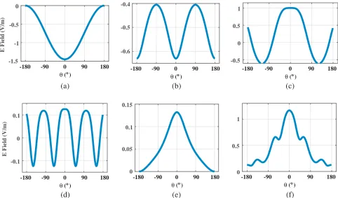
From Equation (21), there is a part that greatly influences the shape of the main lobe and side lobe. If we separate the factors in Eq. (21) as given in Eqs. (22) and (23), different component patterns result as shown in Figure 12.
M L1 = −jE1a
√
πkρ1e−jkr
8r (cosθ+ 1), M L2 = sinφ
cos ka 2 cosθ
ka
2 cosθ
2
−π
2
2, M L3 =e
j k2yρ12k
(22)
SL = F(t1, t2) (23)
Figure 12 displays M L1,M L2,M L3 and SL patterns. As can be seen, multiplication of M L1, M L2,
-1.5 -1 -0.5 0
E Field (V/m) -0.6
-0.5 -0.4 -0.5 0 0.5 1 -0.1 0 0.1
E Field (V/m)
0 0.05 0.1 0.15 0 0.5 1
(a) (b) (c)
(d) (e) (f)
-180 -90 0 90 180
θ ( )o
-180 -90 0 90 180
θ ( )o
-180 -90 0 90 180
θ ( )o
-180 -90 0 90 180
θ ( )o
-180 -90 0 90 180
θ ( )o
-180 -90 0 90 180
θ ( )o
Figure 12. Components of Vivaldi element pattern model: Components of Vivaldi element pattern model: (a) M L1, (b) M L2, (c) M L3, (d) SL, (e) magnitude of multiplication of all components, (f) Magnitude of M Lelements plus SL.
pattern in Figure 12(f). At 3 GHz, if we change the factor θ in ky into 12θ, M L3 in Eq. (22) shows a better performance of E-field. The slope of the tapered slot is changed drastically at the end of the opening mouth of the tapered slot and it yields different phase at the low end of frequency. The resonance at 3 GHz can be shown in upper side of Figure 11(f). However, at 5 GHz, we have to replace theta inkywith 34θ. The slope at the beginning and the middle of the tapered slot impacts the resonance
at high-end frequencies expressed in lower side of Figure 11(f).
Based on the above results, we approximate the modelling E-field of Vivaldi Antenna as:
Eθ ∼=
⎛ ⎜ ⎜ ⎜
⎝K1+K2
⎛ ⎜ ⎜ ⎜
⎝−
jE1a √
πkρ1e−jkr
8r (cosθ+1)
cos ka 2 cosθ
ka
2 cosθ
2
−π
2
2e
j k2yρ12k
⎞ ⎟ ⎟ ⎟
⎠+K3×F(t1, t2)
⎞ ⎟ ⎟ ⎟ ⎠ (24)
t1 = √
s× −K4−K5
1
s
× b1
λ0
×sin (K6θ)
(25)
t2 = √
s× K4−K5
1
s
× b1
λ0
×sin (K6θ)
(26)
where r = 1 m, E = 1 V/m, λg = √λε0r = λ1+ε0 0 2
, a = 0.5λg, b1 = Wt, ρ1 = Lt, K1 = (2.5−0.1f),
K2 = (f+0.3W−0.9),K3 = (2f+0.25W),s= 641 ,K4 = (2−0.3f),K5= (0.9−(0.01W2−0.1W)−0.13f), K6 = 0.9.
-10 0 10 20
E-Field (dBV/m) MSE = 0.35199
-10 0 10 20
MSE = 0.053775
-10 0 10 20
MSE = 0.17622
-10 0 10 20
E-Field (dBV/m) MSE = 0.41352
Modelling result Simulation result Measurement result
-10 0 10 20
MSE = 0.083779
-10 0 10 20
MSE = 0.15416
(a) (b) (c)
(d) (e) (f)
θ ( )o θ ( )o θ ( )o
θ ( )o θ ( )o θ ( )o
-180 -90 0 90 180 -180 -90 0 90 180 -180 -90 0 90 180
-180 -90 0 90 180 -180 -90 0 90 180 -180 -90 0 90 180
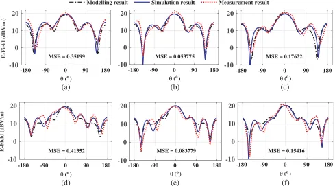
Figure 13. E field in decibel scale on the E-plane at: (a) W = 6 cm, f = 3 GHz, (b) W = 7 cm,
f = 3 GHz, (c) W = 8 cm, f = 3 GHz and (d) W = 4 cm, f = 5 GHz, (e)W = 5 cm, f = 5 GHz, (f)
W = 6 cm,f = 5 GHz.
4. RESULT AND DISCUSSION
4.1. Vivaldi Antenna Element Modelling Result
Figure 13 shows comparison of modelling, simulation, and measurement results in decibel scale of (Eθ)
as given in Eq. (24). Figures 13(a)–(c) show agreement between simulation and modelling for element widths 6 cm, 7 cm, and 8 cm at 3 GHz and so do Figures 13(d)–(f) for element widths 4 cm, 5 cm, and 6 cm at 5 GHz. There are more side lobes at 5 GHz than at 3 GHz. The wider the element is, the smaller the side lobe level is, as shown in Figures 13(a) and (c). The Fresnel equation in Eq. (24), which depends on t1 and t2, greatly influences the shape of the side lobe. By adjusting the constantsK4, K5, and K6
in Eqs. (25)–(26), the number and level of side lobes can be controlled, with t1 and t2. Figure 13 also
demonstrates that increasing frequency will increase the level of the main lobe, which can be controlled by adjustingK3 in Eq. (24). Figure 13(d) shows the asymmetry of side lobe from simulation, which is
caused by the asymmetrical feeding structure, whereas the approximation model shows a symmetrical pattern because it is modeled witht1 =t2. When it is required to model asymmetrical side lobe,t1 and t2 should be designed with non identical constants.
We use the value of Mean Square Error (MSE) to measure the accuracy of a model with our simulation results. The smallest MSE is obtained for antenna element withW = 7 cm, andf = 3 GHz is 0.053775, while the largest MSE is obtained for W = 4 cm, and f = 5 GHz is 0.41352. Figure 14 presents the results of the S11 measurement using a Vector Network Analyzer and radiation pattern
measurement with a spectrum analyzer.
(a) (b)
Figure 14. (a)S11 measurement and (b) radiation pattern measurement.
Table 2. Comparison of modelling and simulation result.
frequency f = 3 GHz
Parsmeter W = 6 cm = 0.6λ W = 7 cm = 0.7λ W = 8 cm = 0.8λ
Result in Modelling Simulation Modelling Simulation Modelling Simulation MainLobe (dBV/m) 19.15 19.5 19.55 19.8 19.94 19.9
3 dB BW (Deg) 62 65.4 62 63.5 62 61.1
1st SLL (dB) −5.53 −4.2 −5.93 −4.8 −6.1 −5.1 Backlobe (dB) 13.44 15.23 13.49 14.97 13.78 14.82
frequency 5 GHz
Parsmeter 4 cm = 0.67λ 5 cm = 0.83λ 6 cm = 1λ
Result in Modelling Simulation Modelling Simulation Modelling Simulation Main Lobe (dBV/m) 19.68 19.3 19.98 20.1 20.27 20.5
3 dB BW (Deg) 68 68.6 58 58 60 53.3
1st SLL (dB) −6.75 −4.3 −6.44 −5.6 −6.82 −6.1 Baclobe (dB) 12.5 14.9 12.53 14.5 12.62 14.31
4.2. Variation Variable of Vivaldi Antenna Modelling
Coefficients a, ρ1, K1-6 in Eqs. (24), (25), and (26) can influence the E field performance. Figure 15
shows the differences in performance ofE-field when ais varied for an antenna with fixed dimensions, in this case L = 6 cm, W = 6 cm at the frequency of 3 GHz. Coefficient a influences the elevation of main lobe, SLL, and beamwidth. In general, the larger the value of a is, the higher the main lobe is, and the smaller the beamwidth is. The main lobe fora= 0.8λg, which is the largest examined herein for 3 GHz frequency, is larger than those for others. It is also shown that while the beam width is the smallest, there are no changes in back lobe level. In addition, the higher the value ofais, the shallower the null of the first side lobe level is as shown in Figure 15. Coefficientρ1 is related with phase variation
in each frequency and responsible for the main lobe and side lobe performance. The greater the value of ρ1 is, the higher the level of main lobe is, and the greater the number of side lobes is as shown in
Figure 16. Comparison between ρ1 = 0.25 and ρ1 = 14.25 shows that higher values of ρ1 yield more
side lobes. Changes in value of coefficient K1 in Eq. (24) shift the overall curve upwards as shown in
Figure 17. Higher values ofK1 lead to higher levels of the main lobe, side lobe level, back lobe, and first
null. The higher the value ofK2 is in Eq. (24), the significantly higher the level of main lobe, side lobe,
-10 0 10 20 30 40
E-field (dBV/m)
a = 0.2λg a = 0.5λg a = 0.8λg
θ ( )o
-180 -90 0 90 180
Figure 15. Modelling result of E-field on the
E-plane with variation of parameter a.
-5 0 5 10 15 20 25
ρ1 = 0.25 ρ1 = 4.25 ρ1 = 12.25
θ ( )o
-180 -90 0 90 180
E-field (dBV/m)
Figure 16. Modelling result of E-field on the
E-plane with variation of parameter ρ.
-10 -5 0 5 10 15 20 25
K1 = 1.8 K1 = 2.8 K1 = 3.8
θ ( )o
-180 -90 0 90 180
E-field (dBV/m)
Figure 17. Modelling result of E-field on the
E-plane with variation of parameter K1.
-10 -5 0 5 10 15 20 25
K2 = 1.9 K2 = 3.9 K2 = 6.9
θ ( )o
-180 -90 0 90 180
E-field (dBV/m)
Figure 18. Modelling result of E-field on the
E-plane with variation of parameter K2.
-5 0 5 10 15 20 25
K3= 1 K3= 7.5 K3= 15
θ ( )o
-180 -90 0 90 180
E-field (dBV/m)
Figure 19. Modelling result of E-field on the
E-plane with variation of parameter K3.
-10 -5 0 5 10 15 20 25
K4= 0.2 K4= 1.1 K4= 2
θ ( )o
-180 -90 0 90 180
E-field (dBV/m)
Figure 20. Modelling result of E-field on the
Figure 19 and Figure 20 present the impact of changes in the values ofK3andK4on Equations (24)
and (25), respectively. Incremental values of K3 and K4 can increase main lobe, side lobe, and back
lobe. The higher values of K3 and K4 result in the shallower null of the first and second side lobe
levels ofE-field performance. Variation in the Fresnel function is shown in Figures 20–22. Parametert1
greatly influences the side lobe on the right side, so doest2on the left side. The number of side lobes can
be changed by varying the constant K5. Enlarging the value ofK5 will reduce beamwidth and increase
the number of side lobes, but maintain the level of main lobe and back lobe. Increasing the number of side lobes can be done by enhancing the value of K5 in the bracketted part of t1 and t2 in Eqs. (25)
and (26), respectively. Figure 22 shows the different phases of side lobe and different nulls of side lobe by maintaining the level of main lobe. Reducing the value of K6 can extend the beamwidth of the
side lobe. Based on Eqs. (24)–(26) and the results in Figures 15–22, another model of Vivaldi antenna element can be developed according to its feeding shape, radiator shape, and operating frequency.
-5 0 5 10 15 20
K5= 0.25 K5= 0.75 K5= 1.5
θ ( )o
-180 -90 0 90 180
E-field (dBV/m)
Figure 21. Modelling result of E-field on the
E-plane with variation of parameter K5.
-5 0 5 10 15 20
K6= 0.8 K6= 0.9 K6= 1
θ ( )o
-180 -90 0 90 180
E-field (dBV/m)
Figure 22. Modelling result of E-field on the
E-plane with variation of parameter K6.
5. APPLICATION TO ARRAY PATTERN MULTIPLICATION
The total array pattern of a Uniform Linear Array (ULA) can be obtained by multiplication of the element pattern and array factor. Figures 23–24 compare the total array patterns between modelling and simulation result. The modelling result is obtained from multiplication of the Vivaldi element model found from Equations (24)–(26) and the factor array.
APtot =Eθ×AF (27)
whereAPtot is total array pattern,Eθ the element pattern, and AF the array factor of the antenna
AF =
N
n=1
wnejψn (28)
wn = anejδn (29)
ψn = kdnsinθ+β (30)
k = 2π/λ (31)
βn = −kdnsinθ0 (32)
wherewn is the complex weight for element,N the number of elements, ψthe progressive phase of the n-th element,dthe element separation, andβn the phase excitation difference.
-10 0 10 20 30
E-field of Total Array Pattern (dB)
Modelling result Simulation Result
θ ( )o
-180-150 -120-90-60 -30 0 30 60 90120 150180
Figure 23. Total array pattern on the E-plane at 3 GHz,N = 4,W = 6 cm.
-10 0 10 20 30
E-field of Total Array Pattern (dB)
Modelling result Simulation result
θ ( )o
-180-150 -120-90-60 -30 0 30 60 90120 150180
Figure 24. Total array pattern on the E-plane at 5 GHz,N = 4,W = 6 cm.
0 2 4 6 8 10
Elemen Pattern (V/m)
W = 40 mm, f = 5 GHz W = 60 mm, f = 3 GHz W = 80 mm, f = 3 GHz
0 1 2 3 4
Array Factor
0 10 20 30 40
Total Array Pattern (V/m)
-40 -20 0 20 40
Total Array Pattern (dBV/m)
(a) (b)
(c) (d)
-180 -90 0 90 180
θ ( )o
-180 -90 0 90 180
θ ( )o
-180 -90 0 90 180
θ ( )o
-180 -90 0 90 180
θ ( )o
Figure 25. E-field pattern on the E-plane for different widths: (a) Element pattern, (b) array factor with d=W, (c) total array pattern (linear scale), (d) total array pattern (dB scale), withN = 4 and no spacing between element.
Figures 25(a) and (b) shows the impact of different element widths to the total linear array pattern. In the same frequency, increasing element width can enlarge mainlobe of total array pattern which can be observed in Figure 25(c) for element width of 6 cm and 8 cm. Antennas with element width of 4 cm at 5 GHz have higher main lobe of total array pattern than element width 6 cm at 3 GHz for the same number of elements. It results from antenna with element width 4 cm has higher gain than antenna with element width 6 cm.
Overall, using the approximation model of the Vivaldi element pattern, one can flexibly achieve array pattern analysis involving arbitrary number of elements and various forms of array, while at the same time saving the computation time. The only difference from the numerical result of electromagnetic computation approach is the absence of mutual coupling impact, which means that the modelling approach approximates the simulation result when mutual coupling between elements is negligible, i.e., when element spacing is sufficiently large.
6. CONCLUSIONS
We have analyzed the impact of variation in various parameters of a Vivaldi antenna, including the element width, the length of tapered slot, the mouth opening of tapered slot, and the opening rate of tapered slot, on such performance indicators as VSWR, resistance, reactance, and radiation pattern. VSWR, impedance, andE-field performances for various geometries can be used as a reference to design a Vivaldi antenna element. Although Vivaldi antenna can be designed with VSWR less than 2 in ultra-wideband frequency, it yields a different performance of radiation pattern in each operating frequency. Following the analysis, we have also found an approximation model of electric field of a Vivaldi antenna element having element width of more than 0.5λand less than 1λat 3 GHz and 5 GHz. The modelling result can be used further to analyze the pattern of a total array with varying number of elements and various array forms by pattern multiplication. This method reduces the computation time and increases flexibility in design and evaluation of Vivaldi antenna array with a large number of elements as long as the effect of mutual coupling is negligible.
ACKNOWLEDGMENT
This work has been supported by the BPPDN (Beasiswa Pendidikan Pascasarjana Dalam Negeri) funding program.
REFERENCES
1. Gibson, P. J., “The Vivaldi aerial,” Proc. 9th European Microwave Conf., 101–105, 1979.
2. Natarajan, R., J. V. George, M. Kanagasabai, L. Lawrance, B. Moorthy, D. B. Rajendran, and M. Alsath, “Modified antipodal Vivaldi antenna for ultrawideband communication,” IET
Microwaves, Antennas &Propagation, Vol. 10, No. 4, 401–405, 2016.
3. Ma, K., Z. Zhao, J. Wu, S. M. Ellis, and Z.-P. Nie, “A printed Vivaldi antenna with improved radiation patterns using two pairs of eye-shaped slots for UWB applications,” Progress In
Electromagnetics Research, Vol. 148, 63–71, 2014.
4. Wang, P., H. Zhang, G. Wen, and Y. Sun, “Design of modified 6–18 GHz balanced antipodal Vivaldi antenna,” Progress In Electromagnetics Research C, Vol. 25, 271–285, 2012.
5. Fioranelli, A., S. Salous, I. Ndip, and X. Raimundo, “Through-the-wall detection with gated FMCW signals using optimized patch-like and Vivaldi antennas,”IEEE Trans. Antennas Propag., Vol. 63, No. 3, 1106–1116, 2015.
6. Yang, Y., Y. Wang, and A. E. Fathy, “Design of compact Vivaldi antenna arrays for UWB see through wall applications,” Progress In Electromagnetics Research, Vol. 82, 401–418, 2008.
8. Natarajan, R., M. Kanagasabai, and J. V. George, “Design of X-band Vivaldi antenna with low radar cross section,”IET Microwaves, Antennas &Propagation, Vol. 10, No. 6, 651–655, 2016. 9. He, S. H., W. Shan, C. Fan, Z. C. Mo, F. H. Yang, and J. H. Chen, “An improved Vivaldi antenna
for vehicular wireless communication systems,” IEEE Antennas Wireless Propag. Lett., Vol. 13, 1505–1508, 2014.
10. Moosazadeh, M., S. Kharkovsky, J. T. Case, and B. Samali, “UWB antipodal Vivaldi antenna for microwave imaging of construction materials and structures,” Microwave and Optical Technology
Letters, Vol. 59, No. 6, 1259–1264, 2017.
11. Esmati, Z. and M. Moosazadeh, “Reflection and transmission of microwaves in reinforced concrete specimens irradiated by modified antipodal Vivaldi antenna,” Microwave and Optical Technology
Letters, Vol. 60, No. 9, 2113–2121, 2018.
12. Moosazadeh, M., “High-gain antipodal Vivaldi antenna surrounded by dielectric for wideband applications,” IEEE Trans. Antennas Propag., Vol. 66, No. 8, 4349–4352, 2018.
13. Nurhayati, G. Hendrantoro, T. Fukusako, and E. Setijadi, “Mutual coupling reduction for a UWB coplanar Vivaldi array by truncated and corrugated,” IEEE Antennas Wireless Propag. Lett., Vol. 17, No. 12, 2284–2288, Dec. 2018.
14. Shin, J. and D. H. Schaubert, “A parameter study of stripline-fed Vivaldi notch-antenna arrays,”
IEEE Trans. Antennas Propag., Vol. 47, No. 5, 879–886, May 1999.
15. Chio, T. H. and D. H. Schaubert, “Parameter study and design of wide-band widescan dual-polarized tapered slot antenna arrays,” IEEE Trans. Antennas Propag., Vol. 48, No. 6, 879–886, 2000.
16. Nurhayati, G. Hendrantoro, and E. Setijadi, “Effect of Vivaldi element pattern on the uniform linear array pattern,”IEEE International Conference on Communication, Networks and Satellite, 42–47, 2016.
17. Nurhayati, G. Hendrantoro, and E. Setijadi, “Total array pattern characteristics of coplanar Vivaldi antenna in E-plane with different element width for S and C band application,” Progress In
Electromagnetics Research Symposium Abstracts, 604–612, Singapore, Nov. 19–22, 2017.
18. Schaubert, D. H., “Wide-band phased arrays of Vivaldi notch antennas,”International Conference
on Antennas and Propagation, 6–12, Apr. 1997.
19. Mailloux, R. J., Phased Array Antenna Handbook, Artech House, Boston, London, 2005.
20. Reid, E. W., L. O. Balbuena, A. Ghadiri, and K. Moez, “A 324-element Vivaldi antenna array for radio astronomy instrumentation,” IEEE Trans. Antennas Propag., Vol. 61, No. 1, 241–249, Jan. 2016.
21. Kindt, R. W. and W. R. Pickles, “Ultrawideband all-metal flared-notch array radiator,” IEEE
Trans. Antennas Propag., Vol. 58, 3568–3575, Nov. 2010.
22. Vescovo, R., “Constrained and unconstrained synthesis of array factor for circular arrays,” IEEE
Trans. Antennas Propag., Vol. 43, 1405–1410, Dec. 1995.
23. Florence, P. V. and G. S. N. Raju, “Optimization of linear dipole antenna array for sidelobe reduction and improved directivity using APSO algorithm,” IOSR Journal of Electronics and
Communication Engineering, Vol. 9, 17–27, 2014.
24. Mohammadian, H., N. M. Martin, and D. W. Griffin, “A theoretical and experimental stufy of mutual coupling in microstrip antenna arrays,” IEEE Trans. Antennas Propag., Vol. 37, 1217– 1223, Oct. 1989.
25. Janaswamy, R. and D. H. Schaubert, “Analysis of the tapered slot antenna,”IEEE Trans. Antennas
Propag., Vol. 39, No. 9, 1058–1065, Sep. 1987.
26. Janaswamy, R. and D. H. Schaubert, “Characteristic impedance of wide slotline on low-permitivity substrate,” IEEE Trans. on Microwave Theory and Techniques, Vol. 34, 900–902, Sep. 1986. 27. Balanis, A. C.,Antenna Theory Analysis and Design, John Wiley & Sons, Arizone State University,
![Figure 1. Dimension of a Vivaldi antenna [16], with R is opening slope/opening rate of tapered slot.](https://thumb-us.123doks.com/thumbv2/123dok_us/1881996.1245285/2.612.167.456.566.689/figure-dimension-vivaldi-antenna-opening-slope-opening-tapered.webp)