Modelling and Simulation of p-i-n Quantum Dot Semiconductor
Saturable Absorber Mirrors
Ahmed E. AbouElEz1, *, Essam ElDiwany1, Mohamed B. El Mashade2, and Hussein A. Konber2
Abstract—Semiconductor saturable absorber mirror (SESAM) based on InAs quantum dot (QD) material is important in designing fast mode-locked laser devices. A self-consistent time-domain travelling-wave (TDTW) model for the simulation of self-assembled QD-SESAM is developed. The 1-D TDTW model takes into consideration the time-varying QD optical susceptibility, refractive index variation resulting from the intersubband free-carrier absorption, homogeneous and inhomogeneous broadening. The carrier concentration rate equations are considered simultaneously with the travelling wave model. The model is used to analyze the characteristics of 1.3-µm p-i-n QD InAs-GaAs SESAM. The field distribution resulting from the TDTW equations, in both the SESAM absorbing region and the distributed Bragg reflectors, is obtained and used in finding the device characteristics including the modulation depth and recovery dynamics. These characteristics are studied considering the effects of QD surface density, inhomogeneous broadening, the number of QD absorbing layers, and the applied reverse voltage. The obtained results, based on the assumed device parameters, are in good agreement, qualitatively, with the experimental results.
1. INTRODUCTION
Semiconductor saturable absorber mirror (SESAM) is a highly reflecting device structure consisting of a semiconductor saturable absorber integrated with distributed Bragg reflector (DBR). This device is used for passively mode-locked lasers. A saturable absorber (SA) is an optical material in which the absorption of the active material decreases (i.e., the material is saturated) with the increase of the incident optical field intensity. The mechanism of SA can be explained as follows; when a semiconductor is illuminated by light with sufficient photon energy, electrons are excited from the valence band to the conduction band. For low optical field intensity, the degree of excited carriers is small, and the absorption of the semiconductor remains unsaturated. At sufficiently high optical field intensity the absorption decreases because electrons can accumulate in the conduction band, accompanied by depletion in the valence band. As a result, the reflectivity of the device increases. This feature can be used in producing narrow pulses in mode locking by suppressing low-intensity levels in the pulse thus reducing the pulse width.
Quantum dot (QD) structures are at present one of the most favourable materials for the design of SAs that have been employed in a wide range of ultrafast laser systems, transforming them into more compact and reliable ultrashort pulse laser sources. SESAMs based on QD materials allowed implementation of the first mode-locked integrated external-cavity surface emitting laser (MIXSEL) [1]. SESAMs based on QD structures have several advantages over quantum well (QW) based counterparts such as a broadband absorption spectrum, due to the inhomogeneous broadening associated
Received 28 November 2017, Accepted 1 March 2018, Scheduled 11 March 2018 * Corresponding author: Ahmed E. Abouelez ([email protected]).
1 Microwave Engineering Department, Electronics Research Institute, Cairo, Egypt. 2 Electrical Engineering Department, Faculty
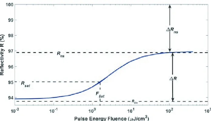
Figure 1. Parameters defining the reflectivity of a QD-SESAM as a function of the incident pulse fluence.
with the distribution of the dot sizes. Furthermore, fast absorption recovery dynamics are helpful for forming and sustaining ultrashort pulses and are necessary to obtain high repetition rate laser pulses. Also, SESAMs based on QD structures have lower saturation fluence and hence, have potentially attractive features in respect of the generation of shorter pulses.
Figure 1 shows the nonlinear reflectivity Rof the SESAM versus the incident pulse energy fluence
Fp. The result shown in the figure is under the assumption of flat-top incident field [2]. The reflectivity
is defined as the ratio of the energy of the reflected pulse and the energy of the incident pulse [3]. The SESAM has several important parameters, shown in Figure 1. The most important parameter is the modulation depth ΔR, which is defined as the difference in reflectivity between a fully saturated and an unsaturated SESAM. Other important parameters are the nonsaturable losses ΔRns and the
saturation fluenceFsat. The saturation fluence is the fluence required for the SESAM to begin absorption
saturation. The pulse energy fluence is the incident pulse energy per unit surface area, Fp = Ep/A.
As shown in Figure 1, Rlin is the linear reflectivity for pulses with very low pulse energy fluence (i.e.,
unsaturated SESAM case), Rns is the reflectivity for high pulse energy fluences when SA is bleached.
The modulation depth ΔR is equal to the difference betweenRns and Rlin and ΔRns= 1−Rns is due
to the internal losses in the SESAM. The reflectivity corresponding to the saturation fluence Fsat is
Rsat which is calculated as Rsat =Rlin+ [ΔR/exp(1)] [2]. The definitions above imply that Rlin and
Rns are not experimentally accessible but extrapolated values from the measured data using a proper
model function [2].
The modulation depth has an important effect on the mode-locking from the point of view of pulse width and stability. It is found that the pulse width is inversely proportional to the modulation depth [3]. To achieve shorter pulses with minimum requirements for self-starting mode-locking, the high modulation depth is required. An upper limit for the modulation depth is dictated by the mode-locking stability requirement (i.e., to prevent the onset of Q-switched mode-locking).
Another important parameter of the SESAM is the absorption recovery dynamics. The recovery dynamics affect the pulse width of mode-locked lasers. To achieve efficient short pulse formation in high repetition rate mode-locked lasers, fast recovery dynamics is required. The most important parameter that influences the recovery dynamics of p-i-n QD-SESAM is the reverse applied voltage [4, 5].
charac-teristics of self-assembled 1.3-µm InAs-GaAs QD-SESAM. In the analysis, the field distribution in the SESAM together with the carrier concentration rate equations are used. In this model, the detailed structure of Bragg reflector and the absorber region and the lateral field distribution of the fundamen-tal mode have been considered. The time-varying QD optical susceptibility, refractive index variation resulting from the intersubband free-carrier absorption, homogeneous and inhomogeneous broadening are taken into consideration. The effects of the reverse voltage, QD surface density, inhomogeneous broadening, and number of QD layers on the modulation depth and the recovery dynamics are taken into consideration.
The paper is organized as follows: in Section 2, the device under investigation is described. In Section 3, the theoretical model is presented, which includes the basic formulas of material parameters. The one-dimensional travelling wave model is developed and the wave propagation through the Bragg mirror is described. Exciton multi-population rate equations for the carrier dynamics are described and linked to the travelling wave model. In Section 4, the modulation depth and recovery dynamic characteristics of the QD-SESAM under consideration are explored. Finally, the conclusions are presented in Section 5.
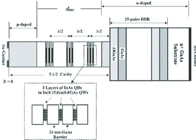
2. P-I-N QD-SESAM STRUCTURE
The QD-SESAM structure under investigation is similar to, but not the same as the one described in [12]. As shown in Figure 2, the SESAM device is a 5λ/2 resonance cavity embedded between a top reflector formed by the Fresnel reflection at the semiconductor/air interface, which is typically 30%, and bottom DBR. This SESAM design is called low-finesse Fabry–Perot resonance structure [3]. The structure is a p-i-n junction. The SESAM structure having a p-i-n junction permits the control of the saturable absorption characteristics through the application of a reverse voltage bias [12], thus, it acts as an actively controlled saturable absorber mirror. The cavity consists of 3 stacks of InAs QD sheets embedded in In0.15Ga0.85As QWs (i.e., dot-in-a-well (DWELL)). Each stack consists of 3 layers
of DWELL separated by 33 nm GaAs barrier. The cavity is terminated by n-doped DBR mirror. The
DBR mirror consists of 25 pairs of GaAs/Al0.9Ga0.1As. Al0.9Ga0.1As has a lower refractive index, while
GaAs has a higher refractive index. The 25 pairs are terminated by a half pair of the lower refractive index, which is not shown in Figure 2. The first layer of the DBR seen from the inner cavity is assumed to be manufactured from Al0.98Ga0.02As, which is used to create 20-nm AlO3 native oxide aperture
of diameter equal to the SESAM aperture. The SESAM aperture radius is assumed to be 80µm. The purpose of oxide aperture is to make a kind of wave index-guiding. AlO3 is assumed to have a
refractive index of 1.5296. Due to the presence of the oxide layer, the field is confined radially, and the device has a step index-guided structure in the radial direction between the core, of the aperture diameter, and the cladding [13]. Core refractive index is the refractive index of the layer material, while cladding refractive index is lower than that of the core because of the presence of the oxide layer with low refractive index. Finally, the absorption loss coefficient in each layer of the device is assumed to be as follows [14]; 1.6457 cm−1, 1.1861 cm−1 for (n-Al0.9Ga0.1As/n-GaAs), respectively. 0.85 cm−1,
3.0428 cm−1 for (p-Al0.9Ga0.1As/p-GaAs), respectively. For i-GaAs barrier, the loss is assumed to be
5 cm−1.
3. THEORETICAL MODEL
The theoretical model constitutes two parts; the travelling wave equations describing the dynamic field variation along the device and the rate equations that describe the carrier dynamics. In order to study the reflectivity and the recovery dynamics of the SESAM, these parameters are studied with an incident pulse on the SESAM with an applied reverse voltage.
3.1. Travelling Wave Equations
At fixed wavelength (i.e., operating wavelength at λo = 1.3µm) and assuming the lateral distribution
of the field to be the fundamental linearly polarized LP01 mode [15, 16], the electric field along the
proposed laser structure in z-direction as a function of time t can be represented as a superposition of two slowly varying envelopes,AF(z,t) and AB(z,t), of the forward and backward propagating waves of the carrier frequency. The slowly varying envelope of the electric field can be shown to satisfy the following travelling wave equation in the longitudinalz direction for each of the forward and backward traveling waves [9–11];
±∂AF /B(z, t)
∂z +
n
eff
c
∂AF /B(z, t)
∂t
= −αi 2 A
F /B(
z, t)−jωo
c ΔnF−effA
F /B(
z, t)−
j1
2
ωo
cneff
PeffF /B(z,t) (1)
In non-active regions, the last two terms do not contribute. neff is the mode effective refractive
index in each dielectric layer in the structure, where mode propagation constant βo =koneff, and ko is
the free space propagation constant [15, 16]. cis the speed of light. The effective refractive index of the mode can be calculated in terms of the difference between the core and the cladding refractive indices. Core refractive index is the refractive index of the layer material, while cladding refractive index is lower than that of the core because of the presence of the oxide layer with low refractive index. The effective difference between core and cladding refractive indices is calculated according to the method described in [13] which has a value of 0.0168. The fundamental mode effective refractive indices in the different materials are calculated to be 3.4109, 2.9514, 3.4504, and 3.4128 for GaAs, Al0.9Ga0.1As, DWELL
Layer, and Cavity (i.e., GaAs barrier & DWELLs), respectively. αi is the internal loss coefficient in
each layer, ωo the angular frequency corresponding to operating wavelength λo, ΔnF−eff the refractive
index variations which result from the intersubband free-carrier absorption (FCA), and PF /B(z,t) the slowly varying effective (forward/backward) dynamic polarization term of the active region.
In the follows, the different factors affecting the travelling wave equations are described.
3.1.1. Treatment of Inhomogeneous Broadening
the whole QD system [17]. In order to obtain the susceptibility of the QDs with corresponding different resonant energies, the whole QD ensemble is subdivided into n = (2N + 1) discrete groups separated by energy difference of ΔE. The resonant energies forith QD confined state (GS, ES1, and ES2) of the nth QD group are given by En,i=Ei−((N+1)−n)ΔE, where Ei is the interband resonant energy
of the central group. The inhomogeneous broadening due to the fluctuation in QD size distribution is usually described by Gaussian distribution G(En,GS) around the center energy EGS for the ground
state, which holds also for any confined stateEi [17]. The full-width at half maximum (FWHM) of the
inhomogeneous broadening is the same for all confined states. The existence probability of thenth QD group is approximately given byGn=G(En,GS)ΔE where
nGn= 1 andEn,GS is the transition energy
for each group ofGS. The transition energy for theGS is assumed to be 0.9616 eV, which corresponds to 1.3-µm radiation, while the energy differences between the other states of the considered self-assembled InAs QDs structure in the conduction band are as those given in [9] (see Figure 3).
(a) (b)
Figure 3. (a) Schematic of the energy band diagram of the dot-in-a-well layer under no applied reverse voltage, (b) under applied reverse voltage [9].
3.1.2. Polarization Term
The polarization is the convolution of the susceptibility and the field. The polarization can be expressed as a summation over all QD groups forGSasPF /B=ΓRΓZ
n p F /B
n,GS, where ΓRis the relative confinement
factor for the device stacks, also called gain enhancement factor, which accounts for the effect of positioning the stacked absorbing layers at field antinodes [15]. Γz=(nl−stackda)/(2Δz), wherenl−stack
is the number of active layers per stack,dais the active layer thickness and (2Δz) is equal to a thickness
of half wavelength in the device surrounding an active stack [11]. pF /Bn,GS can be calculated as a function
of device radius as follows [9, 10, 17];
pF /Bn,GS = jCn,GS(2ρn,GS(r,t)−1)I F /B
n (z,t) (2a)
Cn,GS = DGSN3DGn
q2π|PGSσ | 2
εom2oωo
1
πΓcv
(2b)
ρn,i = Nn,i
DiN3DGn,i
=GS (2c)
+ΓcvΔt
2 A
F /B(
z,t) +AF /B(z,t)ej(ωGS,n−ωo)Δt
e−ΓcvΔt
(2d)
where, Cn,GS is a constant factor,ρn,ithe occupation probability of thenth QDs group andith energy
levels,Nn,ithe carrier density in theith QD confined state of thenth QD group, andDithe degeneracy
of the ith QD energy level assumed to be 2, 4, 6 forGS, ES1, and ES2, respectively [9]. The carrier density will be obtained by the solution of the rate equations as will be described in the electrical model. In Eq. (2b), (N3DGn) gives the QD volume density in thenth QD group, where N3D=Nsd/hQD is the
QD volume density,Nsd the QD surface density per layer, andhQD the average QD height. Along with
this,qandεoare the electron charge and permittivity of free space, respectively. |PGSσ |2is the momentum
matrix element [17]. The momentum matrix element|PGSσ |2 is calculated equal to 2.9848×10⁻³⁰kg eV.
In Eq. (2b), 1/Γcv represents the characteristic dephasing time of the interband transition which is related to FWHM of the homogeneous broadening by Fhom= 2Γcv. The FWHM of the homogeneous
broadening is assumed to be 18 meV at 300 K.InF /B(z,t) in Eq. (2a) represents the convolution integral
between the complex Lorentzian function in the time domain and (forward/backward) slowly varying field amplitude, which represents time domain filtering of the field by the Lorentzian function [9]. ωGS,n
is the radial frequency corresponding to the interband resonant energy of groupnofGS.
3.1.3. Free Carrier Absorption Term
The field equations are affected also by the refractive index variations which result from the intersubband free-carrier absorption (FCA), calculated as a function of time and device radius atωo according to the
relation given in [11, 18];
ΔnF(r,t,ωo) =− q 2
2neffεoω2o
⎡ ⎣Γz
⎛
⎝NW (r,t)
m∗eW
+
n,i
Nn,i(r,t)
m∗eD
⎞
⎠+ΓBNB
(r,t)
m∗eB
⎤
⎦ (3)
whereNBandNW are the carrier densities in the barrier and QW, respectively. meD∗ ,m∗eW, andm∗eBare
the electron effective masses of QD, QW, barrier materials, respectively. The electron effective masses of the GaAs barrier, In0.15Ga0.85As QW, and InAs QD are (0.0665)mo, (0.06)mo, and (0.023)mo [19],
respectively.
3.1.4. Effective Parameters and Gain Suppression Coefficient
For any radially dependent parameterX, such as optical susceptibility or refractive index change due to the intersubband transitions, an effective value of the parameter is used in thez-directional travelling wave equation, which is weighted by the lateral distribution of the field through the following relation
Xeff=
∞
0 X(r)|ψN(r)|
2rdr[7]. The normalized fundamental transverse mode distribution|ψ
N(r)|2 has
a dimension of [1/m2] [11].
To take into account the nonlinear absorption suppression, the polarization term given by Eq. (2a) is further multiplied by a factor of the form 1/(1+εcS(r,t)), whereεc [m3] is the nonlinear gain coefficient,
which is a function of FWHM of the homogeneous broadening and the photon lifetime [17]. The nonlinear gain coefficient is calculated to be 1.0603×10⁻²⁴m3 at T = 300 K [17]. S(r,t) is the photon density inside the cavity which can be calculated simply from the energy density of the electric field through the following relation [11, 20];
S(r,t) =
εon2eff
2ωo
AF (z,t)2+AB(z,t)2
|ψN(r)|2 (4)
As will be described in the electrical model section, Eq. (4) can be considered as a link between the travelling waves amplitudes and stimulated emission term in the rate equations.
3.2. Numerical Solution of the TDTW Equations and the Boundary Conditions
The distribution of AF /B(z,t) along the absorber cavity and the DBRs can be represented in the
number of dielectric layers. The thickness of the ith dielectric layer is assumed equal to Δzi, where i
is an integer, and the position of the boundary between the ith and (i−1)th layers is zi. Dielectric
layer thickness Δzi is varied according to its effective refractive index such that the layer length deltaz
is equal to a quarter wavelength (λo/(4neff(i))) which is a necessary condition for the operation of the
DBR. A suitable choice for the relation between time and spatial steps in thezdirection in the solution of Eq. (1) is Δt= (Δzineff(i)/c), and Δtwill be a constant time step. In the simulation, the traveling
waves, AF /B(z,t), are advanced from one dielectric interface at time t to the next interface at t+ Δt. Across active layers, where the QD stacks are placed, Eq. (1) can be solved with the first-order finite difference approximation, as follows [11];
AF(zi+Δzi,t+Δt) = AF(zi,t) +
−αi
2 −jkoΔnF−eff(t)
AF(zi,t) Δzi−jPeffF (zi,t) Δzi (5a)
AB(zi,t+Δt) = AB(zi+1,t) +
−αi
2−jkoΔnF−eff (t)
AB(zi+1,t) Δzi−jPeffB (zi+1,t) Δzi(5b)
At the interfaces between two layers, boundary conditions are applied. At each time step, the boundary conditions for reflection and transmission are applied to the propagating fields at the dielectric interfaces by using Eq. (6). The amplitudes of propagated fields, AF /Bout in terms of the incident fields
and AF /Bin at the boundary between the dielectric layers, can be determined using the transfer matrix as follows [11, 16];
AFout
ABout
=
t11 r12
r21 t22
AFine−jϕ
ABine−jϕ
(6)
where the corresponding transmission coefficients are t11=2neff(i−1)/(neff(i)+neff(i−1)); and the
corresponding reflection coefficients are r12=−r21=(neff(i)−neff(i−1))/(neff(i)+neff(i−1)); neff(i−1)
are the effective refractive indices of the mode in adjacent ith and (i−1)th layers, respectively. As stated in the previous section, AF(z,t) and AB(z,t) slowly vary with respect to both z andt; however,
the operation of the DBR requires that the length of each of its layers must be quarter wavelength. Thus, a phase shift of ϕ = (π/2) across the layer is included in Eq. (6). Thus the amplitudes (i.e.,
AF(z,t) and AB(z,t)) slowly vary with respect to time, whereas they include the phase variation with
z as described. The boundary conditions at the top and bottom surfaces of the Bragg reflectors can be written as;
AB(t, zk+1) =rRAFin(t, zk+1)
AF(t, z1) =ABin(t, z1)rL+
1−rL2 Pin(t) √
μo/εo
(7)
The reflectivity and recovery dynamics of the SESAM are studied for an incident pulse, thus the instantaneous pulse power incident on the SESAM aperture Pin(t) is introduced in the boundary
condition at the sesam-air interface. The pulse has temporal Gaussian shape with defined energy
Ep and FWHM duration time τp, assuming an incident optical pulse transverse distribution matching
the LP01transverse distribution in the device. In Eq. (7), rL is semiconductor-air reflectivity at z= 0.
The semiconductor-air reflectivity rL = 0.55 and semiconductor-metal reflectivity rR = −0.974. The
output power is calculated according to the following equation [11, 20];
Pout≈cωo
εo
2ωo
AB out(z1)
2
(8)
3.3. Electrical Model and Rate Equations of Carrier Density in the Saturable Absorber
3.3.1. Effects of Revers Voltage
The applied reverse voltage causes the formation of a triangular barrier as shown in Figure 3(b). Due to the applied reverse voltage, the barrier height energy is lowered by ΔEL = hQD·q·F/2 [4] where
hQD is the QD height and F the electric field caused by reverse biase voltage which is perpendicular
to the p-i-n junction. This electric field is calculated as F = (Vr+Vbi)/dint, where Vr is the applied
reverse voltage, Vbithe built-in potential assumed to be 0.8 V [4], anddint the intrinsic region length in
the cavity.
The main effects influencing the carrier dynamics under an applied reverse voltage are enhanced thermionic escape rates from the QD ES2 to the QW and from QW to barrier state which are due to a linear barrier reduction induced by the applied voltage. For high applied reverse voltage, the width of this barrier may decrease sufficiently to allow carriers to tunnel from theGS,ES1, and ES2 and the QW directly to the 3-D states in the barrier, shown by horizontal arrows in Figure 3(b).
A weak quantum confinement Stark effect (QCSE) in QD structures has also been observed compared with QW structures [4]. For simplicity, this weak QCSE will be neglected in our model, whereas the influence of the applied field on both thermionic and tunneling escape processes will be properly introduced using simple approaches.
Expressions for the tunneling escape rates from the QD confined k states (i.e., krefers to the nth group of each ith confined state GS,ES1, andES2) and from the QW to the 3-D states in the barrier can be expressed for a triangular well as follows [4];
Rtun k = ftunexp
−4 3
2m∗eB(ΔEB−k)3/2
qF
(9a)
Rtun W = ftunexp
−4 3
2m∗eB(ΔEB−W)3/2
qF
(9b)
The tunneling rates given by Eqs. (9a)–(9b) are calculated by multiplying the barrier collision frequency ftun = π/2m∗h2QD of the carriers in QD/QW with the barrier transmission probability
(the exponential term), which is estimated by Wentzel-Kramer-Brillouin approximation [4]. m∗eB is the
electron effective mass of GaAs barrier, andm∗ is the electron effective mass of QD/QW material [9]. The reverse voltage affects also enhances thermionic escape rates as will be indicated later.
3.3.2. Carriers Rate Equations
The rate equations describe the carrier density dynamics in different energy levels. Carriers are generated in the confined GS level by the pulse injection with photon energy tuned to theGS transition of the QD. The generated carriers are then transferred between the energy states by relaxation, capture, escape, and tunneling, and then disappear by current drift from the barrier and by carrier recombination.
The dynamics of carrier density as a function of the radius in the device are presented in a set of rate equations. The first rate Eq. (10a) is for carrier density NB in the 3-D barrier state. The second
rate Eq. (10b) describes carrier densityNW in the 2-D QW state Finally. There arenrate Eqs. (10c)–
(10e) for the carriers (electrons for exciton model) densityNn,i in theith QD state of thenth QD group
as follows [9];
dNB(r,t)
dt = −μBNB
V +Vbi
d2 int
+ NW
τW−B−
1
τB−W
(1−ρW) +
1
τB r
NB
+RtunWNW +
k
Rtun kNk (10a)
dNW(r,t)
dt = NB
τB−W
(1−ρW) +
n
Nn,ES2
τn,ES2−W−
NW
τW−ES2
n
(1−ρn·ES2)Gn
− NW
τW−B−
1
τW r
dNn,ES2(r,t)
dt =
NWGn(1−ρn,ES2)
τW−ES2
+ Nn,ES1
τES1−ES2
(1−ρn·ES2)− N n,ES2
τES2−ES1
(1−ρn,ES1)
−Nn,ES2
τES2−W
(1−ρW)−Nn,ES2ρn,ES2
τES2 Aug
−Nn,ES2
τES2 r
−Rtun n,ES2Nn,ES2 (10c)
dNn,ES1(r,t)
dt =
Nn,ES2
τES2−ES1
(1−ρn,ES1) + Nn,GS
τGS−ES1
(1−ρn,ES1)− Nn,ES1
τES1−GS
(1−ρn,GS)
− Nn,ES1
τES1−ES2
(1−ρn,ES2)−N
n,ES1ρn,ES1
τAugES1
−Nn,ES1
τES1 r
−Rtun n,ES1Nn,ES1 (10d)
dNn,GS(r,t)
dt =
Nn,ES1
τES1−GS
(1−ρn,GS)− Nn,GS
τGS−ES1
(1−ρn,ES1)
−Nn,ES1ρn,ES1
τGS Aug
−Nn,ES1
τGS r
−Rtunn,GSNn,GS+Rgeneration,n (10e)
The first term in Eq. (10a) accounts for the electron drift current from the barrier to the bias circuit under applied reverse voltage. μB is the electron mobility of the GaAs barrier material which
is given byμB= 7200(300/T)2.1cm2/V·s [19]. ρW is the occupation probability in the QW state [19].
Rtun k andRtun W are the tunnelling rates from the QD states and QW to the barrier which are given
by Eqs. (9a) and (9b), respectively. τB−W is the carrier capture time to the QW and is assumed to be
0.3 ps [9, 21]. The enhanced thermionic escape time from the QW to the barrier state can be modelled as follows [9];
τW−B(V) =
τB−WDOSWhWnl
DOSBdint
exp
ΔEB−W
kBT
exp
−ΔEL(V)
kBT
(11a)
where DOSB is the effective density of states per unit volume in the GaAs barrier [11]. DOSW is the
effective density of states per unit volume in the QW layer [11]. dint is the intrinsic region length as
shown in Figure 2. τrB and τrW are the carrier recombination times in GaAs barrier and InGaAs QW,
respectively. Their values are assumed to be 400 ps [21]. In Eq. (10b),τW−ES2is the average relaxation
time from QW to ES2 while τn,ES2−W is the enhanced thermionic escape time from ES2 to QW for
each QD group, given by [9];
τn,ES2−W(V) =
τW−ES2DES2N3D
DOSW
exp
Δ
E(W−n,ES2)
kBT
exp
−ΔEL(V)
kBT
(11b)
ΔE(W−n,ES2)is the energy difference between QW band edge andES2 energy levels of thenQD groups
in the conduction band. DES2 is the degeneracy ofES2.
The carrier density Nn,i in the ith QD state of thenth QD group is related to the corresponding
occupation probability via Eq. (2c). The carrier lifetime inGS,ES1, andES2 are denoted byτrGS, τrES1
and τrES2, respectively. The carrier lifetime for all QD states is assumed equal to 1 ns [19]. The
characteristic Auger recombination times, τAugi with i = GS, ES1, ES2 of QD confined states, are
assumed to have values of 660, 270, and 110 ps, respectively [9, 21].
It is assumed that relaxation and capture times between energy levels exist only between adjacent states. Carriers relaxation time from QW to ES2 is expressed asτW−ES2 = 1/(Ac+CcNW) which is
assumed to be identical for all groups [22]. The average intradot relaxation times from the QD ith to
jth level with subscriptsi,j=GS,ES1,ES2 can be expressed, with the hypothesis that the final state is empty, asτi−j(i=j) = 1/(Ao+CoNW) [19, 22]. Ac andAo are the phonon-assisted relaxation rates,
whileCc and Co are the Auger relaxation rates. The values of Ac and Cc are assumed to be 1×10¹²s−1
and 1×10⁻¹⁴m3s−1, respectively. Ao and Co are assumed to be 5×10¹¹s−1 and 3.5×10⁻¹³m3s−1,
respectively [22].
Furthermore, there is an exponential relationship between the relaxation times and escape scape times in QD confined states. The escape times from confined stateito confined statej can be obtained in terms of relaxation times from confined stat j to confined state ias follows [9, 19];
τ(i−j)=
τ(j−i)D i
Dj
exp
ΔEi−j
kBT
where ΔEi−j is the interband energy difference between two successive levels. The carrier generation
rate term in Eq. (10e) is given by;
Rgeneration,n = ΓR
c neff
ωo
cneffC
GS,n(1−2ρn,GS(r,t))
1 1+εcS(r,t)
×
εon2eff
2ωo
RAF∗(z,t)InF(z,t)
+RAB∗(z,t)InB(z,t)
|ψN(r)|2
(13)
whereR denotes the real part, and the second bracket in the right-hand side represents the absorption while the last bracket includes the photon density of the forward and backward fields together with the Lorentzian function filtering.
4. SIMULATION RESULTS AND DISCUSSION
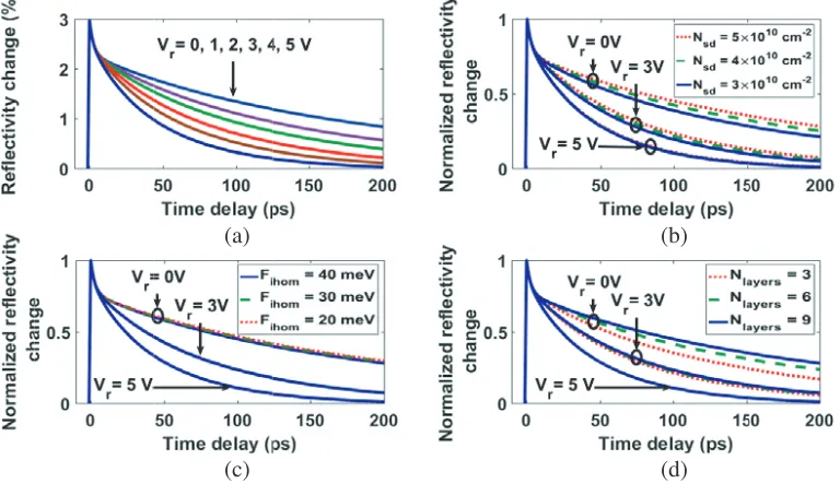
In this section, we will first examine the modulation depth ΔR as a function of different operating parameters such as reverse bias voltage, QD surface density, number of QD absorbing layers, and FWHM of inhomogeneous broadening for the device under consideration described above. The absorption recovery dynamics are then studied considering the effects of the above parameters. The number of QD groups is taken to be 9, and the FWHM of the homogeneous broadening is assumed to be 18 meV at 300 K for all studied cases.
4.1. Modulation Depth ΔR
Gaussian pulses with 130 fs width and energy fluences in the range 0.01–1000µJ/cm2 are incident on the
QD-SESAM. The photon energy of each pulse is tuned to the ground state transition of the QD (i.e., 0.9616 eV). Figure 4(a) shows the reflectivity as a function of pulse energy fluence with different values of applied reverse voltage and a constant value of inhomogeneous broadening of 40 meV. It is noted that the modulation depth ΔR is not affected by the applied reverse voltage. The calculated modulation depth is nearly equal to 3.12% and the saturation fluence Fsat ≈ 0.84µJ/cm2 and non-saturable loss
ΔRns≈0.25%. This result is interpreted by the fact that the applied reverse voltage affects the escape
(a) (b)
(c) (d)
times and accordingly the transient recovery, but does not affect the reflectivity at steady state. Also, the applied reverse voltage results in weak QCSE in QD compared to its effect in QW based SESAM devices. This result is consistent with that obtained experimentally in [5]. The main differences between the result shown in Figure 4(a) under the assumption of LP01 lateral distribution of the field and the
result shown in Figure 1 for flat-top distribution of the field are in the value of ΔRns which is much
smaller for the LP01 case, and in the value ofFsat which is approximately half the value of the flat-top
case [2]. The smaller value of ΔRns may be interpreted to be due to the confined field for the LP01
distribution which leads to lower losses.
One of the methods used to control the modulation depth in QD-SESAM devices is controlling the QD surface density. To examine the effect of QD surface density on the modulation depth, different values of QD surface density of 3×1010cm−2, 4×1010cm−2, and 5×1010cm−2are assumed with constant applied reverse voltage of 3 V and inhomogeneous broadening of 40 meV. As shown in Figure 4(b), as the QD surface density increases the modulation depth increases. Table 1 gives Rlin, ΔR and Fsat
corresponding to each QD surface density value. This result is, qualitatively, in agreement with the experimental work which showed that the modulation depth is proportional to the QD surface density [6]. This result can be explained as follows. The value of the reflectivity of a saturated SESAM Rns is
constant for all QD surface densities. On the other hand,Rlin decreases with increasing the absorption,
which is proportional to the susceptibility (see Eq. (2)), thus by increasing QD surface density, the absorption increases, reflectivity decreases, and accordingly ΔR increases.
Table 1. QD-SESAM parameters at different QD surface density.
Nsd Rlin ΔR Fsat
5×1010cm−2 96.607% 3.12% 0.84µJ/cm2 4×1010cm−2 97.225% 2.5% 0.84µJ/cm2 3×1010cm−2 97.846 % 1.88% 0.84µJ/cm2
Other device parameters can also lead to increasing the modulation depth. As stated above in connection with Eq. (2), the absorption can be increased by increasing the value ofpF /Bn,GSof the QD group
related to the operating wavelength (i.e., center group) by decreasing the FWHM of inhomogeneous broadening. Increasing the number of QD layers leads to a similar result. This can be interpreted as follows. It can be seen from the expression ofPF /B (preceding Eq. (2a)) that the change of the number
of layers affects the values of ΓR and ΓZ, where the effect of ΓZ is more dominant, i.e., as the number
of layers increases the effective polarization PF /B in Eq. (2a) increases, which increases the absorption. The effect of inhomogeneous broadening on the modulation depth is examined for different values of Fihom of 40, 30, 20 meV at constant applied reverse voltage of 3 V and constant surface density of
5×1010cm−2. Figure 4(c) illustrates this effect. It is clear that the linear reflectivity increases with increasing Fihom, and accordingly the modulation depth decreases. Table 2 gives Rlin, ΔR and Fsat
which correspond to each value of inhomogeneous broadening.
Table 2. QD-SESAM parameters at different FWHM values of the inhomogeneous broadening.
Fihom Rlin ΔR Fsat
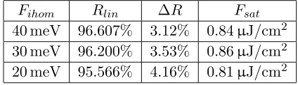
40 meV 96.607% 3.12% 0.84µJ/cm2 30 meV 96.200% 3.53% 0.86µJ/cm2
20 meV 95.566% 4.16% 0.81µJ/cm2
Table 3. QD-SESAM parameters at different values of the number of layers.
Nlayers Rlin ΔR Fsat
3 98.515% 1.22% 0.72µJ/cm2 6 97.409% 2.32% 0.76µJ/cm2 9 96.607% 3.12% 0.84µJ/cm2
that increasing the number of layers increases the value of the modulation depth, as mentioned above. Table 3 gives Rlin, ΔR andFsat for different numbers of QD absorbing layers in the cavity.
4.2. Absorption Dynamics
The absorption recovery dynamics in the experimental work is normally investigated using the pump-probe technique. In this technique, a high intensity short pulse with fluence above Fsat is injected to
the SESAM [4, 5]. The recovery dynamics of the SESAM is monitored by injecting weak probe pulses with variable delay times relative to the pump pulse and monitoring the reflection from the SESAM for these delayed probe pulses. The probe pulse energy in this technique is assumed to be small enough such that the absorption dynamics is not significantly perturbed.
The absorption recovery dynamics using the pump-probe technique is modeled in this section. The pump pulse and probe pulse are assumed to have Gaussian shape and 130 fs width. The pump pulse has a fluence of 10µJ/cm2, which is greater than the saturation fluences calculated in the previous section. The probe pulses have a fluence of 0.01µJ/cm2. The probe pulses are considered to have the same frequency of the pump pulse which is resonant with the GS transition energy. The absorption of the pump pulse with high energy fluence causes the generation of carriers in the QDGS groups, leading to a significant absorption bleaching. The dynamics of reflectivity changes of the probe pulse induced by the pump pulse at different delay time intervalsτ are calculated asdR(τ) =R(τ)−Ro whereRo is the
reflectivity for probe pulses under no applied pump pulse.
At first, the recovery dynamics of the reflectivity change will be examined considering the effect of the applied reverse voltage, as shown in Figure 5(a). The response can be fitted well with three
(a) (b)
(c) (d)
components with different time constants according to the following equation;
dRf itted(τ) =Aexp (−τ /τ1) +Bexp (−τ /τ2) +Cexp (−τ /τ3) (14)
where τ1 corresponds to the fast component time constant,and A is its amplitude. The slow recovery
has two stages with slow time constants τ2 and τ3, respectively. B and C are the amplitudes of these
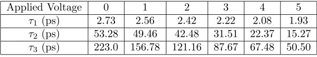
components. Table 4 shows the values of the three time constants for different applied reverse voltages.
Table 4. Fitting time constants for different applied reverse voltages.
Applied Voltage 0 1 2 3 4 5
τ1 (ps) 2.73 2.56 2.42 2.22 2.08 1.93
τ2 (ps) 53.28 49.46 42.48 31.51 22.37 15.27
τ3 (ps) 223.0 156.78 121.16 87.67 67.48 50.50
As shown in Figure 5(a) and Table 4, the fast recovery time constant τ1 changes from 2.73 to
1.93 ps as the applied reverse voltage changes from zero to 5 volt. This time constant is related to the excitation of the photo-generated carriers fromGS to higher energy states ES1 andES2 [9]. It is clear that the absorption recovery dynamics are dominated by the slow time constants τ2 and τ3 which are
highly dependent on the applied voltage. As expected, as the reverse applied voltage increases the slow recovery time constantsτ2 andτ3decrease. This result can be explained in view of Eq. (9) and Eq. (11)
for the thermionic and tunneling processes. As the applied reverse voltage increases, the electric field
F across the QD layers increases which in turn enhances the thermal escaping rate and tunneling rate leading to faster recovery time. The absorption recovery is finally completed as a result of nonradiative recombination and spontaneous emission processes occurring on a time scale of hundreds of picoseconds. The obtained results are consistent with the behavior of the experimental results given in [4–6].
Now, the effect of QD surface density on recovery dynamics will be investigated. Different values of QD surface density of 3×1010cm−2, 4×1010cm−2, and 5×1010cm−2 are assumed. Results are obtained for applied reverse voltage of zero (i.e., the effect of reverse applied voltage is neglected), 3, and 5 volt. The inhomogeneous broadening of 40 meV and the number of QD layers of 9 are constant. Figure 5(b) shows the reflectivity change normalized with respect to its peak value for these assumed conditions. At zero voltage, the effect of QD surface density on the recovery dynamics is maximum, and this effect decreases with increasing the reverse voltage. Table 5 gives the fitting time constants for different values of QD surface density at zero volt. It can be noted from Figure 5(b) and Table 5 that the slow recovery time constants increase as the surface density increases. This result does not agree with the experimental result given in [6]. In [6], the measurement shows that by increasing the QD coverage the recombination becomes faster, and this result is explained by a higher defect density that leads to a faster recombination or a higher interdot transfer probability caused by the smaller distances between the dots. In our model, it is assumed that the carrier lifetime for all QD states and the characteristic Auger recombination times are constant for all assumed QD surface density values. This assumption is considered because of the difficulty of obtaining suitable values for recombination times corresponding to the assumed QD surface density. So, our result, in this case, deviates from the published experimental result.
Table 5. Fitting time constants for different values QD surface density at zero volt.
Nsd(cm−2) 3×10¹⁰ 4×10¹⁰ 5×10¹⁰
τ1 (ps) 2.67 2.71 2.73
τ2 (ps) 40.56 47.11 53.28
τ3 (ps) 168.37 197.40 223.06
Figure 5(c) shows the effect of the inhomogeneous broadening on the recovery dynamics for different values of Fihom of 40, 30, 20 meV at different reverse voltages and constant surface density
of 5×1010cm−2. These effects are considered under the assumption that the carrier lifetime for all QD
broadening. As can be noted from the data in Table 6, at zero volt there is a slight effect on the recovery dynamics for the three values of the inhomogeneous broadening; as the inhomogeneous broadening increases the slow recovery time components increase slightly. At high applied reverse voltage this effect vanishes.
Table 6. Fitting time constants for different values QD inhomogeneous broadening at zero volt.
Fihom (meV) 20 30 40
τ1 (ps) 2.77 2.76 2.73
τ2 (ps) 36.93 45.71 53.28
τ3 (ps) 221.03 222.93 223.06
Finally, the effect of changing the number of QD absorbing layers on the recovery dynamics is shown in Figure 5(d) for different values of layers of 9, 6, and 3 and different applied reverse voltages, where the surface density is 5×1010cm−2. Table 7 shows the fitting time constants at zero volt. At
zero volt, the slow recovery time constants increase as the number of QD absorbing layers increases. At higher applied voltages, this behaviour becomes insignificant. This behaviour can be interpreted as was discussed in connection with the modulation depth, that the increase of the number of QD layers leads to increase of the polarization. This is similar to the increase of the susceptibility which may result from an increase of the QD volume density (Eqs. (2a)–(2b)). This explains the similarity of the effects of QD surface density and the number of layers on the recovery dynamics seen in Figure 5(c) and Figure 5(d).
Table 7. Fitting time constants for different values QD absorbing layers in the cavity at zero volt.
Nlayers 3 6 9
τ1 (ps) 2.52 2.65 2.73
τ2 (ps) 47.91 53.44 53.28
τ3 (ps) 141.93 187.02 223.06
5. CONCLUSION
In this paper, a TDTW model is used to analyze the characteristics of a p-i-n QD-SESAM, namely the modulation depth and the recovery dynamics. The parameters which affect these characteristics are the reverse applied voltage, QD surface density, QD inhomogeneous broadening, and number of QD absorbing layers. The results show that the modulation depth of the SESAM is highly affected by the QD absorbing material parameters. The modulation depth can be increased by increasing the QD surface density, increasing the number of QD absorbing layers, or decreasing the inhomogeneous broadening of QDs. Also, it is found that the modulation depth is not affected by the reverse applied voltage. The recovery dynamics of the QD-SESAM is mainly affected by the applied reverse voltage. It is found that as the applied reverse voltage increases the slow recovery time constants decrease. Under the assumption that the carrier lifetime for all QD states and the characteristic Auger recombination times are constant for all above parameters, it is found that the slow recovery time constants increase by increasing the QD surface density, number of QD absorbing layers, and decreasing the inhomogeneous broadening. The effect of these parameters becomes insignificant as the applied reverse voltage increases.
REFERENCES
1. Bellancourt, A. R., B. Rudin, D. J. H. C. Maas, M. Golling, H. J. Unold, T. Sudmeyer, and U. Keller, “First demonstration of a Modelocked Integrated External-Cavity Surface Emitting Laser (MIXSEL),”2007 Conference on Lasers and Electro-Optics (CLEO), 2007.
3. Keller, U., “Semiconductor nonlinearities for solid-state laser modelocking and Q-switching,” E. Garmire, A. Kost (eds.), Nonlinear Optics in Semiconductors II. Semiconductor and Semimetals, Vol 59, 211–286, Academic Press, San Diego, CA, 1998.
4. Malins, D. B., A. Gomez-Iglesias, S. J. White, W. Sibbett, A. Miller, and E. U. Rafailov, “Ultrafast electroabsorption dynamics in an InAs quantum dot saturable absorber at 1.3µm,”Applied Physics Letters, Vol. 89, No. 17, 171111, 2006.
5. Zolotovskaya, S. A., M. Butkus, R. H¨aring, A. Able, W. Kaenders, I. L. Krestnikov, D. A. Livshits, and E. U. Rafailov, “p-i-n junction quantum dot saturable absorber mirror: Electrical control of ultrafast dynamics,”Optics Express, Vol. 20, No. 8, 9038–9045, Mar. 2012.
6. Maas, D. J. H. C., A. R. Bellancourt, M. Hoffmann, B. Rudin, Y. Barbarin, M. Golling, T. S¨udmeyer, and U. Keller, “Growth parameter optimization for fast quantum dot SESAMs,”Optics Express, Vol. 16, No. 23, 18646–18656, 2008.
7. Yu, S. F., “Dynamic behavior of vertical-cavity surface-emitting lasers,”IEEE Journal of Quantum Electronics, Vol. 32, No. 7, 1168–1179, 1996.
8. Yu, S. F., “An improved time-domain traveling-wave model for vertical-cavity surface-emitting lasers,”IEEE Journal of Quantum Electronics, Vol. 34, No. 10, 1938–1948, 1998.
9. Rossetti, M., P. Bardella, and I. Montrosset, “Time-domain travelling-wave model for quantum dot passively mode-locked lasers,”IEEE Journal of Quantum Electronics, Vol. 47, No. 2, 139–150, 2011.
10. Gioannini, M. and M. Rossetti, “Time-domain traveling wave model of quantum dot DFB lasers,” IEEE Journal of Selected Topics in Quantum Electronics, Vol. 17, No. 5, 1318–1326, 2011.
11. Abouelez, A. E., E. Eldiwany, M. B. El Mashade, and H. A. Konber, “Time-domain travelling-wave model for quantum dot based vertical cavity laser devices,” Progress In Electromagnetics Research M, Vol. 65, 29–42, 2018.
12. Lagatsky, A. A., E. U. Rafailov, W. Sibbett, D. A. Livshits, A. E. Zhukov, and V. M. Ustinov, “Quantum-dot-based saturable absorber with pn junction for mode-locking of solid-state lasers,” IEEE Photonics Technology Letters, Vol. 17, No. 2, 294–296, 2005.
13. Michalzik, R., “Simple understanding of waveguiding in oxidized VCSELs,”Annu. Rep. 1, 19–23, Dept. Optoelectron., Univ. Ulm, Ulm, Germany, 1995.
14. Piskorski, L., M. Wasiak, R. Sarzala, and W. Nakwaski, “Structure optimisation of modern GaAs-based InGaAs/GaAs quantum-dot VCSELs for optical fibre communication,” Opto-Electronics Review, Vol. 17, No. 3, 217–224, Jan. 2009.
15. Mulet, J. and S. Balle, “Mode-locking dynamics in electrically driven vertical-external-cavity surface-emitting lasers,”IEEE Journal of Quantum Electronics, Vol. 41, No. 9, 1148–1156, 2005. 16. Yu, S. F., Analysis and Design of Vertical Cavity Surface Emitting Lasers, John Wiley & Sons,
2003.
17. Sugawara, M., Self-assembled InGaAs/GaAs Quantum Dots: Semiconductors and Semimetals, Vol. 60, Academic Press, San Diego, CA, 1999.
18. Kim, J., C. Meuer, D. Bimberg, and G. Eisenstein, “Effect of inhomogeneous broadening on gain and phase recovery of quantum-dot semiconductor optical amplifiers,” IEEE Journal of Quantum Electronics, Vol. 46, No. 11, 1670–1680, 2010.
19. Tong, C., S. Yoon, C. Ngo, C. Liu, and W. Loke, “Rate equations for 1.3-µm dots-under-a-well and dots-in-a-dots-under-a-well self-assembled InAs-GaAs quantum-dot lasers,” IEEE Journal of Quantum Electronics, Vol. 42, No. 11, 1175–1183, 2006.
20. Agrawal, G. P. and N. K. Dutta, Semiconductor Lasers, 2nd Edition, Van Nostrand, New York, 1993.
21. Xu, T., M. Rossetti, P. Bardella, and I. Montrosset, “Simulation and analysis of dynamic regimes involving ground and excited state transitions in quantum dot passively mode-locked lasers,”IEEE Journal of Quantum Electronics, Vol. 48, No. 9, 1193–1202, 2012.
![Figure 3. (a) Schematic of the energy band diagram of the dot-in-a-well layer under no applied reversevoltage, (b) under applied reverse voltage [9].](https://thumb-us.123doks.com/thumbv2/123dok_us/1918558.1251747/5.612.85.540.241.462/figure-schematic-diagram-applied-reversevoltage-applied-reverse-voltage.webp)