Design and Simulation of 2-Bit Hybrid Adder using GDI
Technique
Deepali Chaudhary
1, Satyendra Sharma
2,Nidhi Sharma
31
ECE Dept., NIET, Greater Noida, UP, India
ABSTRACT
In this paper, a new modified 2-bit hybrid adder is designed using modified full adder cells by CMOS and GDI
technique.The adder is first simulated for 1 bit and is extended for 2-bit adder.The circuit is simulated
usingTanner Tool in 180-and 90-nm technology. Variousperformance parameters like power, delay and power
delay product (PDP) arecalculated, and compared with the existing adder circuits. At 1.8-V supply for 180-nm
technology, the normal power utilization of adder is 2.8545 µw with a minimum delay of 7.2266 ps and for
90-nm technology a power consumption of 0.08 µw with a minimum delay of 13.825 ps is reported at 1.2- V supply
voltage.
Keywords
:
GDI technique, Hybrid adder, Low Power, propagation delay, Complementary MOS,Tanner
I. INTRODUCTION
Decrease in channel length demands a circuit which consume less power and less delay. Full Adder is a combinational circuit that performs the addition of three bits (two significant bits and previous carry). It consists of three inputs and two outputs, two inputs are the bits to be added, the third input represents the carry form the previous position. The output sum is equal to 1 when only one input is equal to 1 or when all three inputs are equal to 1. The Cout output has a carry 1 if two or three inputs are equal to 1. Adder has two modules namely
Over the top power dissipation in incorporated circuits, not just demoralizes their utilization in compact environment additionally causes overheating, diminishes chip life and corrupts execution. Minimizing power dissipation is in this way essential. Power dissipation can be decreased by scaling the supply voltage. The scaling of supply voltage straightly with highlight size was begun from half-micron innovation. Be that as it may, the power supply scaling influences the speed of the circuit .The need of the time is to place endeavors in outlining low-power and high speed circuits.
II. HYBRID 1-BIT FULL ADDER CIRCUIT
Figure.1. detailed circuit diagram of full adder.
The sum output of the full adder is implemented by XNOR modules. The inverter comprised of transistors Mp1 and Mn1 generate B’, which is effectively used to design the controlled inverter using the transistor pair Mp2 and Mn2. Output of this controlled inverter is basically the XNOR of A and B. But it has some voltage degradation problem, which has been removed using two pass transistors Mp3 and Mn3. pMOS transistors (Mp4, Mp5, and Mp6) and nMOS transistors (Mn4, Mn5, and Mn6) realize the second stage XNOR module to implement the complete SUM function. Analyzing the truth table of a full adder, the condition for Cout
generation has been deducted asfollows: If, A = B, then Cout= B; else,Cout= Cin
The parity between inputs A and B is checked by A.B function. If they are same, then Cout is same as B, whichis
implemented using the transmission gate realized bytransistors Mp8 and Mn8. Otherwise, the input carry signal(Cin) is reflected as Cout which is implemented by anothertransmission gate consisting of transistors Mp7
full adder during its actual use in VLSIapplications, a practical simulation environment is setup. To provide a realistic environment, buffers areadded at the input and the output of the test bench .The inputs to the adder cell, are fed through the buffers toincorporate the effect of input capacitance and the outputs arealso loaded with buffers to ensure proper loading condition.The proposed full adder is simulated using several test benchsetups. Further, the behavior of performance parameters (power and delay) could be measured from the second adder cell by using this test bench. This offered the tested adder cell to have the output and input capacitances of adjacent adder cells as its input and output capacitance; allowing a real time simulation environment forcascaded approach. Numerous random signal patterns were applied at the inputs and the worst case simulation results of the second full adder cell was accounted for analysis and comparison. The performance analysis of the proposed full adder was performed with variation in supply voltage both for 180- and 90-nm technology.
II. PROPOSED ADDER
Figure.2proposed Adder circuit.
Main source of power consumption in adder are sum and carry modules.In this proposed work XNOR block is designed using pass transistors with less no. of CMOS and carry block is designed using GDI technique. So it will give less power and delay in circuit with the reduced area occupancy.
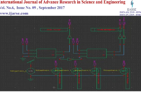
III. 2-BIT ADDER
It is designed by connected modified full adder cell in cascaded form.Output is taken out as S0, S1 using buffer
Figure 3.schemetic of 2- bit adder
IV. RESULT
The proposed Adder cell dissipates less static power during mode transitions due to charge recycling. Low leakage currents and the voltage sources provide better stability. Simulation has been done for power dissipations, access time, leakage current and power delay product for the proposed Adder and the results of the proposed Adder are compared with those of other reported existing adder. Result is carried out in 90nm and 180nm
.
Table 1. Result for 90-nm technology
Parameters Base Modified
Power 0.16065 µw 0.080058µW
Delay
0.014897 ps
13.825 ps
PDP 0.002393 aJ 1.1068 aJ
Table 2. Result for 180-nm technology
Parameters Base Modified
Power 0.68101 µW 0.28545 µW
Delay 5.5312 ps 7.2266 ps
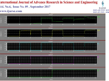
Figure 4. Simulation Result for 90nm Technology
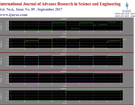
Figure 6. Simulation Result for 180nm Technology
Figure 7. Simulation Result of 2-Bit adder at 180-nm Technology
VI. CONCLUSION
The simulation of full adder cell and 2-bit adder was carried out using standard Tanner EDA tool with 180/90-nm technology and compared with existing design standard design. The simulation results established that the proposed adder offered improved PDP compared with the earlier reports. The efficient XNOR gate with less number of transistor lead to fast switching speeds.GDI technique provide less power consumption with minimum delay and less no. of CMOS. The proposed full adder offered 49.83% improvement with respect to the previous design in terms of Power Consumption (90-nm technology at 1.2 V). Corresponding Power improvement was 41.91% when the same design was implemented in 180-nm technology at 1.8-V power supply.
REFERENCES
[1] C.-K. Tung, Y.-C. Hung, S.-H. Shieh, and G.-S. Huang, “A low-power high-speed hybrid CMOS full adder for embedded system,” in Proc.IEEE Conf. Design Diagnostics Electron. Circuits Syst., vol. 13. Apr. 2007, pp. 1–4.
[2] S. Goel, A. Kumar, and M. A. Bayoumi, “Design of robust, energyefficient full adders for deep-submicrometer design using hybrid-CMOSlogic style,” IEEE Trans. Very Large Scale Integr. (VLSI) Syst., vol. 14, no. 12, pp. 1309–1321, Dec. 2006.
[3] N. H. E. Weste, D. Harris, and A. Banerjee, CMOS VLSI Design: A Circuits and Systems Perspective, 3rd ed. Delhi, India: PearsonEducation, 2006.
[4] J. M. Rabaey, A. Chandrakasan, and B. Nikolic, Digital Integrated Circuits: A Design Perspective, 2nd ed. Delhi, India: Pearson Education,2003.
[5] D. Radhakrishnan, “Low-voltage low-power CMOS full adder,” IEE Proc.-Circuits Devices Syst., vol. 148, no. 1, pp. 19–24, Feb. 2001.
[6] R. Zimmermann and W. Fichtner, “Low-power logic styles: CMOS versus pass-transistor logic,” IEEE J. Solid-State Circuits, vol. 32, no. 7,pp. 1079–1090, Jul. 1997.
[7] C. H. Chang, J. M. Gu, and M. Zhang, “A review of 0.18-μm full adder performances for tree structured arithmetic circuits,” IEEE Trans. VeryLarge Scale Integr. (VLSI) Syst., vol. 13, no. 6, pp. 686–695, Jun. 2005.
[8] A. M. Shams, T. K. Darwish, and M. A. Bayoumi, “Performance analysisof low-power 1-bit CMOS full adder cells,” IEEE Trans. Very LargeScale Integr. (VLSI) Syst., vol. 10, no. 1, pp. 20–29, Feb. 2002.
[9] M. L. Aranda, R. Báez, and O. G. Diaz, “Hybrid adders for high-speed arithmetic circuits: A comparison,” in Proc. 7th IEEE Int. Conf. Elect.Eng. Comput. Sci. Autom. Control (CCE), Tuxtla Gutierrez, NM, USA, Sep. 2010, pp. 546–549.
[10] C.-K. Tung, Y.-C. Hung, S.-H. Shieh, and G.-S. Huang, “A low-powerhigh-speed hybrid CMOS full adder for embedded system,” in Proc.IEEE Conf. Design Diagnostics Electron. Circuits Syst., vol. 13.Apr. 2007, pp. 1–4.
No of transistor Base Modified
[11] S. Goel, A. Kumar, and M. A. Bayoumi, “Design of robust, energyefficientfull adders for deep-submicrometer design using hybrid-CMOSlogic style,” IEEE Trans. Very Large Scale Integr. (VLSI) Syst., vol. 14,no. 12, pp. 1309–1321, Dec. 2006.