ABSTRACT
MAHAJAN, NIKHIL RAVINDRA. System Protection for Power Electronic Building Block Based DC Distribution Systems. (Under the direction of Mesut E Baran)
The purpose of this research has been to develop an agent based protection and reconfiguration scheme for power electronic building block based (PEBB) DC distribution systems. One of the foremost applications would be in the new zonal DC distribution on naval ships. The research involves the design of an agent based protection scheme which uses the PEBBs for current limiting and circuit breaking purposes. Considerations are given to reduce the system downtime under fault conditions, allow proper coordination and provide backup protection. The research also involves the design of a reconfiguration management scheme based on collaborative agents. The collaboration ensures that the reconfiguration is achieved at a global level, enhancing the system survivability under the conditions of multiple faults and damages. The coordination ensures that only the faulted part of the system is isolated and the reconfiguration makes sure that the power to the healthy part of the system is supplied continuously. The reconfiguration management also performs load shedding if the generation does not meet the load demand of the reconfigured system due to a fault or damage in the generator.
Keywords: Agent, Buck converter, Circuit-Breaker, Current-limiting, Distribution, EMTDC, Inverter, PEBB, Protection, PSCAD, Reconfiguration, Rectifier, SES
System Protection for Power
Electronic Building Block Based
DC Distribution Systems
By
Nikhil Ravindra Mahajan
A Dissertation submitted to the Graduate Faculty of North Carolina State University
in partial fulfillment of the requirements for the degree of
Doctor of Philosophy
ELECTRICAL ENGINEERING
Raleigh
November 2004
APPROVED BY:
____________________ ____________________ ____________________ Dr. John J Grainger Dr. Arthur W Kelley Dr. Michael Young
BIOGRAPHY
ACKNOWLEDGEMENTS
I express my deep sense of sincerest gratitude to my advisor and mentor, Dr. Mesut Baran for his support, guidance and advice throughout my graduate program at NCSU.
I thank Dr. Grainger, Dr. Kelly and Dr. Young for serving on my advisory committee, and providing important suggestions, feedbacks and inputs during my program.
I thank Jinsang Kim and Ismail Shaker for providing help, stimulating discussions and maintaining ambience of the lab, conducive for research during the course of the project.
I thank John Nordstrom, Craig Muller and the rest of the PSCAD support team for providing help at various levels with the PSCAD software.
I thank Gautam Ghatnekar for being a good roommate.
I thank the teachers and professors at my undergraduate college in Vallabh Vidyanagar, who instilled my interest to Electrical Engineering.
I also thank my close friends Jalpesh, Sunil and Dimpal with whom I had many stimulating and interesting discussions.
I thank all those, who kept asking me all these years: "Have you finished yet?" Silencing that question was a big motivation when life’s many other attractions kept enticing me.
I thank all those, who may have helped me in any possible way.
I express my appreciation to my family for moral boosting, continued support and most importantly their belief in me, throughout my life.
I express deep appreciation to my beloved for her unwavering love, care and support through the thick and thin. She has been my relentless source of motivation.
TABLE OF CONTENTS
Page
List of Figures... vi
List of Abbreviations ... ix
1 Introduction... 1
1.1 Background ... 1
1.2 Motivation... 4
1.3 Outline... 5
2 Current Limiting DC Circuit Breaker... 7
2.1 Introduction and Overview ... 7
2.2 Fault Current Limiting Circuit Breaker: A Literature Survey ... 8
2.3 PEBB as Current Limiting Circuit Breaker ... 10
2.4 Rectifier Fault Current Limiting CB... 11
2.5 Inverter Fault Current Limiting CB ... 21
2.6 Buck Converter Fault Current Limiting CB ... 25
2.7 Chapter Summary ... 28
3 DC Distribution System Protection... 30
3.1 Introduction and Overview ... 30
3.2 Conventional HVDC Protection: Literature Survey ... 30
3.3 PEBB Based DC SES Protection... 32
3.4 Switch Level Autonomous Protection ... 33
3.5 Agent Based System Protection... 35
3.5.1 Rectifier Fuse for Rectifier AC Zone... 42
3.5.2 CDCCB for Primary DC Zone... 44
3.5.3 Rectifier Agent... 45
3.5.4 Buck Converter Agent ... 67
3.6 Agent Based System Protection: Co-ordination & Backup... 80
3.7 Chapter Summary ... 89
4 Reconfiguration Management ... 90
4.1 Introduction and Overview ... 90
4.2 Agent Based Collaborative Reconfiguration ... 90
4.2.1 Objectives and Requirements ... 90
4.2.2 Contingencies... 91
4.2.3 Agent Based Reconfiguration... 91
4.3 Chapter Summary ... 103
5 Conclusions... 104
5.1 Contributions... 104
5.2 Future Research ... 105
6 References... 107
7 Appendices... 110
Appendix A Fuse Selection For Rectifier Protection ... 111
Appendix B Buck Converter Design Considerations... 117
LIST OF FIGURES
Page
Figure 1 : Simple Single Bus 2 Zone DC Distribution System ... 2
Figure 2 : DC Zonal Electrical Distribution System (also, SES)... 5
Figure 3 : Hybrid Fault Current Limiting Circuit Breaker ... 9
Figure 4 : Rectifier as a Typical PEBB... 11
Figure 5 : VSC IGBT Anti-Parallel Diode Switch Realization ... 12
Figure 6 : VSC as a Diode Bridge Under Fault Condition ... 12
Figure 7 : Bi-Directional Current Control Switch Realization ... 13
Figure 8 : Fault Handling by Operating Switch in Saturation Region... 14
Figure 9 : Voltage and Current Stress under High Impedance Fault... 15
Figure 10 : Equivalent Circuit of ETO ... 16
Figure 11 : ETO Circuit Symbol... 16
Figure 12 : ETO Snubberless Turn-Off Capability... 17
Figure 13 : Switch Realization with IGBT and Anti-Parallel ETO Device... 17
Figure 14 : Modified Rectifier PEBB Topology... 18
Figure 15 : Rectifier Shutdown... 20
Figure 16 : Generator Currents ... 20
Figure 17 : PWM Inverter with Associated Filters... 21
Figure 18 : Inverter PEBB Current Limiting ... 23
Figure 19 : ETO and Diode Currents... 24
Figure 20 : Branch (Device) Voltages ... 24
Figure 21 : Inverter Input Current... 25
Figure 22 : Full Bridge Buck Converter ... 25
Figure 23 : Modified Full Bridge Buck Converter ... 26
Figure 24 : Branch (ETO) Currents ... 28
Figure 25 : Voltage across Branches (ETO) ... 28
Figure 27 : Hierarchical Protection for the DC SES... 33
Figure 28 : ETO Gate Drive Circuit for Over-Current Protection... 34
Figure 29 : Over-Current Protection Waveforms for ETO... 34
Figure 30 : DC SES with Circuit Breakers ... 36
Figure 31 : Zones of a DC SES... 38
Figure 32 : Fuse Operation ... 43
Figure 33 : CDCCB Protection... 44
Figure 34 : Protection Zones around Rectifier PEBB... 46
Figure 35 : AC and DC Faults close to Rectifier PEBB ... 46
Figure 36 : Simulation Results of Rectifier DC Bus fault ... 49
Figure 37 : Simulation Results of Rectifier DC Rail fault... 51
Figure 38 : Shoot-Through Fault ... 53
Figure 39 : Sustained Shoot-Through Fault... 54
Figure 40 : Simulation Results of DC Bus to Ground Fault ... 56
Figure 41 : Simulation Results of L-L fault before Inductor ... 59
Figure 42 : Simulation Results of L-L Fault after Inductor... 61
Figure 43 : Simulation Results of 3-Phase Fault ... 63
Figure 44 : Simulation Results of Phase C to Ground Fault... 66
Figure 45 : Protection Zones around Buck Converter PEBB ... 67
Figure 46 : Faults close to Buck Converter PEBB ... 68
Figure 47 : Secondary DC Bus Fault Simulation Results... 70
Figure 48 : Load Side DC Rail Fault simulation results... 71
Figure 49 : Shoot-Through Fault Simulation Results... 72
Figure 50 : Transformer Primary Side Fault Identification ... 73
Figure 51 : Transformer Secondary Side Fault Detection ... 73
Figure 52 : Source Fault Detection ... 74
Figure 54 : Protection Zones around Inverter PEBB ... 77
Figure 55 : Faults close to Inverter PEBB ... 78
Figure 56 : Typical Protection for Voltage-fed Inverter... 78
Figure 57 : Fully Protected PWM-VSI Inverter with 4 Current Sensors and One Snubber... 79
Figure 58 : Prototype DC SES for Protection System Co-ordination... 84
Figure 59: Prototype System Circuit Diagram in PSCAD... 84
Figure 60 : Remote Backup Protection by Fuses... 85
Figure 61 : Remote Backup by RAs for a Transformer Primary Fault... 86
Figure 62 : Buck converter SLAP Failure during a Secondary DC bus zone fault ... 87
Figure 63 : Remote Backup by RAs for a Secondary DC Zone Fault... 89
Figure 64: SES with Three Generator Configuration ... 93
Figure 65 : Intra Zonal Bus Configuration ... 94
Figure 66 : Prototype System for Reconfiguration ... 98
Figure 67 : Reconfiguration Results for Primary DC Bus Fault... 101
Figure 68 : Reconfiguration Results for Secondary DC Bus Fault... 103
Figure 69 : Fuse Characteristics... 113
Figure 70 : Cut Off Current Characteristics... 113
Figure 71 : I2t Values ... 114
Figure 72 : Prototype System in PSCAD... 121
Figure 73 : Rectifier PEBB in PSCAD... 122
Figure 74 : Buck Converter PEBB in PSCAD... 122
LIST OF ABBREVIATIONS
I = 10-6, micro, a prefix
A Ampere, unit symbol abbreviation for current
AC Alternating Current
BCA Buck-Converter Agent
BCIS Buck Converter Inverting Stage
BCRS Buck Converter Rectifying Stage
CB Circuit Breaker
CSC Current Source Converter
CSD Controlled Semiconductor Device
DC Direct Current
DCCB Direct Current Circuit Breaker
EMTDC Electro-Magentic Transient DC Program
EMTP Electro-Magnetic Transient Program
ETO Emitter Turn-Off Thyristor
F Farad, unit symbol abbreviation for capacitance
FBSOA Forward Biased Safe Operating Area
FCLCB Fault Current Limiting Circuit Breaker
Flt Fault
Gnd Ground
GTO Gate Turn-Off Thyristor
H Henry, unit symbol abbreviation for inductance
HVDC High Voltage Direct Current
Hz Hertz, unit symbol abbreviation for frequency
IA Inverter Agent
IGBT Integrated Gate Bipolar Transistor
IGCT Integrated Gate Commutated Thyristor
IGCT Integrated Gate Controlled Thyristor
k = 103, kilo, a prefix
L-G Line to Ground
L-L Line to Line
m = 10-3, milli, a prefix
M = 106, mega, a prefix
MOSFET Metal Oxide Semiconductor Field Effect Transistor
MOV Metal Oxide Varistor
NC Normally Closed
NO Normally Open
PCFF Power-Factor Correction with Fixed Frequency
PEBB Power Electronic Building Block
PSCAD Power System Computer Aided Design
PTC Polymer Temperature Controlled
PWM Pulse Width Modulation
RA Rectifier Agent
RBSOA Reverse Biased Safe Operating Area
RMS Root Mean Square
s Second, unit symbol abbreviation for time
SCR Silicon Controller Rectifier
sec abbreviation for second
SEM Semiconductor Unit
SES Shipboard Electrical System
SLAP Switch Level Autonomous Protection
SLP System Level Protection
SOA Safe Operating Area
TCC Time-Current-Characteristics
V Volts, unit symbol abbreviation for Voltage
VSC Voltage Source Converter
Xmer Transformer
1 INTRODUCTION
The main focus of this dissertation is the investigation of protection issues related to the new power electronic building block (PEBB) based DC distribution systems. One of the main challenges for protection against faults in the DC electrical systems is the unavailability of fast DC circuit breakers. Present day DC systems, therefore, still employ conventional devices such as AC side circuit breakers, fuses and/or crowbars for protection purposes. These circuit breakers and fuses are relatively slow and result in considerable system downtime.
In the PEBB based DC distribution, the PEBBs are multifunctional modules which are expected to perform power conversion, monitoring and limiting current and protecting the system during faults. Therefore, the PEBBs can take over the circuit breaker functions and eliminate separate circuit breakers (CB). Investigation of the feasibility of this functionality for the PEBB has been one of the main focuses of this dissertation. The second part of the dissertation involved the design of an agent based system protection scheme to detect and locate the faults that may occur on these new PEBB based DC distribution systems.
Following the fault isolation, a reconfiguration of the unfaulted part of the system is desired. The dissertation proposes a reconfiguration management scheme which minimizes the number of system components left without power following the fault isolation by the agent based system protection scheme.
1.1 Background
Modern power electronic (PE) devices such as power Metal Oxide Semiconductor Field Effect Transistor (power MOSFET), Insulated Gate Bipolar Transistor (IGBT), and Emitter Turn Off device (ETO) have the ability to monitor, limit and interrupt high currents [3]. These features of the modern PE devices, to monitor, limit and interrupt currents allow them to be potentially used simpler protection schemes. This is especially true now, when IGBTs and likes are fast replacing thyristors and SCRs in the medium-high power range. The PEBBs employ IGBTs or the newer ETOs in a voltage source converter topology as opposed to the thyristor based current source converter topology. These PEBBs are connected to each other and to the generation and loads to make up a DC power distribution system, and thus envision the whole power handling system within standardized blocks [4].
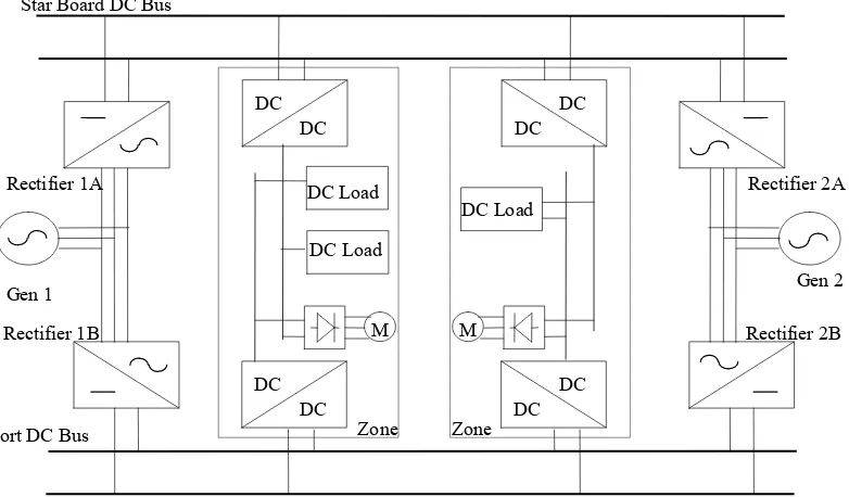
Present day HVDC systems are typically employed in back-to-back configuration or in a multi-terminal configuration connected by DC lines. In contrast to these present day systems, a new zonal architecture has been proposed for distribution of power by DC to relatively concentrated loads such as industrial parks, loads onboard ships, and other high concentration loads. This new zonal DC distribution architecture comprises of the interconnected standardized PEBB blocks feeding power to the loads via one or more DC buses [5]. In this new DC distribution architecture, the loads are divided into zones and each zone consists of physically closely located loads. A simple single bus zonal DC electrical distribution system with two load zones is shown in Figure 1.
Figure 1 : Simple Single Bus 2 Zone DC Distribution System
In the new DC distribution, the PEBBs are used to convert power from AC to DC, convert voltage from one level to another, commensurate with the loads and also convert power back
from DC to AC. The PEBBs also perform frequency conversion and power conditioning.
There are many advantages inherent to such a PEBB based DC power distribution system. First, the PEBBs are multifunctional modules and are expected to perform power conversion, monitoring and limiting current and protecting the system during faults. Thus, DC zonal electrical distribution system will facilitate fault isolation [6]. Since the monitored quantities are DC values, the current sensors and algorithms required to detect the fault conditions are both simpler and faster. As a result, the fault detection and interruption can be achieved much faster.
A second advantage of zonal DC distribution is that variable speed motor control is readily available to many pumps and blowers to operate these devices at the highest efficiencies. In addition substantial inrush currents experienced when starting large motors may be limited or even eliminated, aiding in maintenance of a stable bus voltage. Furthermore, since the PEBBs can perform voltage conversion and current limiting and interruption, the distribution transformers and switchgear may be eliminated. This offers considerable benefit in terms of weight size and cost.
In these modern DC distributions systems, the PEBBs are expected to perform multiple functions like power flow control and voltage transformation, etc [6]. In addition, these modules are also expected to perform monitoring and limiting the current through semiconductor devices, and suitably protecting the system during fault conditions [6], thus opening new avenues for protection. The typical voltage source converter topology that is employed in the present day converters cannot perform current limiting and interruption functions, therefore do not meet the expectations. Therefore additional external devices such as circuit breakers fuses and/or crowbars are needed or protection. These circuit breakers and fuses are relatively slow and result in increased system downtime.
proper protective action for interruption of different faults on the system, and (d) the reconfiguration of the system to maintain continuity of the supply to the loads.
1.2 Motivation
Recent advances in Voltage Source Converter (VSC) technology has made possible for power to be transmitted and distributed by DC. HVDC light systems based on VSCs are now even available in the market for power ranging from as low as few 100s of KVA to the order of 100s of MVA. The U.S. Navy is also presently investigating the implementation of DC Zonal Electrical Distribution System, also called Shipboard Electrical System, SES, for its next generation ships to replace the current AC radial distribution system [6, 7]. The SES is a typical example of the PEBB based DC distribution system. A prototype SES as shown in Figure 2 is based on the PEBB concept which realizes the complete power system in standardized converter building blocks. The DC distribution on the SES allows for the decoupling of the generator frequency from the loads, and thereby allowing the generators and the various loads to operate at their highest efficiency. This results in cost, weight and size optimizations [8]. Thus the advantages of using zonal DC distribution for power onboard ships includes cost savings, elimination of switchgear for protection and isolation without sacrificing performance or safety requirements.
The new DC distribution systems, such as the SES, would essentially comprise of the various interconnected PEBB modules, with the protection functions still performed by relatively slow acting mechanical circuit breakers on the AC side. Investigations were performed, which suggested the feasibility of combining circuit breaker functions into the PEBB modules. We propose to eliminate separate mechanical circuit breakers and perform the current limiting and circuit breaking by the PEBBs themselves, thereby meeting the expectations of the PEBBs set forth earlier. This change would also lend itself to cost, size, weight, maintenance and space reductions as envisioned in [8]. The PEBB based circuit breakers, by their very fast time of operation would reduce the system down-time and provide better continuity of service to the loads of the system.
in the new era of power electronics based DC electrical distribution systems.
Figure 2 : DC Zonal Electrical Distribution System (also, SES)
One of the important issues that need special consideration from the protection and safety perspective is the system grounding. From the point of view of detection of faults, higher currents are easy to detect, but for safety reasons, the ground currents on the SES need to be limited to a low value. The generator grounding impedance plays an important role in minimizing these ground currents. Therefore, investigations were performed to select the type of grounding (solid, low impedance, high impedance or isolated) for the zonal DC SES such as the one shown in Figure 2. Investigations were also performed to determine the ground loop interaction of generators sharing the same ground [9-11] . It was shown that when the generators are solidly grounded, large ground circulation currents of the order of 100A flow through the generator neutrals. It is also indicated in [11], that high impedance grounding of the generator neutral gives a compromise between the ground loop currents, safety and protection. Therefore, the zonal DC SES as shown in Figure 2 is high impedance grounded.
1.3 Outline
Chapter 2 starts with laying down the requirements of a CB and follows it up with a review DC
DC
DC Load
DC DC
DC Load
M M
Rectifier 2A Star Board DC Bus
Rectifier 1A
Gen 1 Gen 2
Zone Zone DC
DC
DC DC Port DC Bus
Rectifier 2B Rectifier 1B
of the state-of-the-art on current limiting circuit breakers. It then proposes to unify the concept of the PEBB and circuit breaking and explains the required switch modifications needed in order to use the PEBB as current limiting circuit breaker. The chapter considers three typical converters, the rectifier, the inverter and the buck converter, for the purpose of current limiting and circuit breaking. It uses simulations to substantiate the claims.
Chapter 3 introduces protection at system level followed by a survey of present HVDC protection schemes. It defines system protection as applicable to the DC distribution system under consideration – the DC zonal SES. The chapter further presents the principles of agent based system protection. Specifically, it details the detection principles and protective actions of the rectifier Protection-Agent, the Buck Converter Protection-Agent and the Inverter Protection-Agent. Simulation results are provided to demonstrate the detection and operation principles. In addition to the detection principles, the chapter also deals with the coordination and backup requirements. The chapter concludes with the demonstration of the operation of backup protections for some of the important faults on the DC SES.
Chapter 4 investigates the issues relevant to the problem of system reconfiguration due to faults, damages and material casualty on a DC zonal SES. It explains the main issues that need consideration for the reconfiguration management scheme to provide uninterrupted supply to all the loads subsequent to the detection and protection action of the protection scheme. The main design issues are the choice of number of generators, choice of number of sectionalizers, location of the sectionalizers, and the intra zonal secondary DC bus configuration. The chapter then explains the operation of the reconfiguration management under different contingencies such as generation failure, multiple faults, etc. Finally, simulation results for two of the main contingencies are provided to demonstrate that the reconfiguration management can seamlessly transfer power to the load from the main supply bus to the alternate supply bus.
2 CURRENT LIMITING DC CIRCUIT BREAKER
2.1 Introduction and Overview
With the introduction of different types of converters into the AC systems, protection issues related to fault interruption emerged. To protect the system against the non self-extinguishing DC faults, a need for DC circuit breakers (DCCB) was immediately felt. Protection philosophies from AC system protections drifted into the protection of these new mixed AC-DC systems and fault interruption was done by employing high voltage high power AC circuit breakers on the AC side. The use of AC circuit breakers (ACCB), therefore deferred the development of the high power DCCB. Low cost alternatives for fault interruption involving crowbars and fuses were also borrowed from AC protections. In addition to this, the ability to control the complete converter delayed the development of DCCB.
The advent of complete gate controllable silicon based solid state devices like the GTO, IGCT and ETO, stimulated the development of the DCCB. Various types of DCCBs based on such devices have been reported in literature [12-16].
The principal function of a CB is to interrupt short circuit current under fault conditions. All the same, under normal/non-fault operating conditions it should also carry the normal rated load current with high efficiency. Thus, the main requirements for a CB are [17]:
(1) The CB should be able to interrupt a short circuit current, normal rated current, or lower, and interrupting this current quickly without causing an abnormal voltage.
(2) The CB should be good conductors and have low voltage drop and losses, withstand normal currents as well as short circuit currents, thermally and mechanically.
(3) The CB should withstand the short circuit for a certain time required to decide whether it is a sustained or a transient fault and whether to interrupt the circuit or not.
(4) When open, the CB should be excellent insulators, and withstand the normal as well as the transient voltages between phases and phase to ground.
Thus, for the new solid state DC circuit breakers to be put to practical use and to operate successfully, these new solid-state-device based circuit breakers must provide at least the same level of functionality as mentioned above and that has been provided by the AC circuit breakers, while still operating at high efficiency.
The following sub-section describes one of the state-of the art hybrid DC circuit breaker which performs these functions successfully.
2.2 Fault Current Limiting Circuit Breaker: A Literature Survey
In the early days of HVDC, there was no need for DCCB, when all transmissions were point-to-point, allowing complete control of current by converter action, even under fault. In principle, the same approach is valid for multi-terminal HVDC systems as well. However, it would be necessary to shut-down the entire system in order to isolate and remove a fault from any branch of a multi-terminal current source converter (CSC) based DC system. This situation encouraged the development of DCCB, which, with or without converter control action (depending on their design) can switch out or return parts of the system [18]. This section reviews one of the state-of-the-art DC fault current limiting circuit breaker (FCLCB).
Modern semiconductor devices like GTO, IGBT and IGCT are now available with moderate to high current and voltage ratings. They also have very robust short circuit Safe Operating Area [19], and in combination with metal-oxide varistors, they have started competing with the thyristor based CBs. Novel concepts for FCLCB have been proposed in recent literature [14, 16, 20].
A hybrid arrangement of 3 different parallel paths for fault current limiting and interruption is presented in [14]. The hybrid FCLCB consists of 3 parallel paths, path A as shown in Figure 3, consists of a fast operating mechanical transfer switch, path B consists of a semiconductor unit & a fast disconnecting switch and a third path C consists of a current limiting impedance (with positive temperature coefficient) and a load switch. Since a single GTO can carry the current only in one direction, it is installed with a four-Diode Bridge to save costs (see D1 to D4 of path B in Figure 3), thus providing unipolar conditions for the
Figure 3 : Hybrid Fault Current Limiting Circuit Breaker
The operation of the FCLCB is discussed here in brief. When a fault occurs, the ultra fast transfer switch (FTS) opens within a few hundred Is and produces an arc voltage drop of several tens of volts. However, the arc voltage is much too small for the purpose of short-circuit current limitation. Therefore, a gate-turn-off thyristor (GTO) with high–current turnoff capability is employed to force the fault-current onto limiting impedance (path C).
Under normal operation, all three switches (FTS, FDS, and LS) are closed. When a fault occurs, the FTS is triggered by a separate sensing and control unit within 50Is. Due to contact separation of the FTS, an arc voltage of approximately 40V builds up across the opening double-contact gap. Since the on-state voltage drop across the SEM (which is connected in parallel to the FTS) of typically 10 to 15V, is smaller than the arc voltage, the current starts to commutate from path A onto path B. To ensure complete current commutation within a short time interval <100Is, the self-inductance of the loop A-B must be sufficiently low on the order of 0.5IH for the given current ratings. Such a low inductance can be achieved through close connection of the paths A and B using compact design.
Approximately 150Is later, the GTO is turned off, forcing the current onto the PTC-resistor in path C. Turning off the GTO causes a very high di/dt , and thus, an excessive voltage rise due to the self-inductance of the loop B-C (on the order of 10IH). As a consequence, the voltage uSjumps up to approximately 4.5kV, and a further rise is limited by the metal-oxide
peak of the current through the semiconductors (ISEM) exceeds the rating of a single GTO, so
that two GTOs connected in parallel were chosen.
When the current is completely transferred onto the PTC-resistor the massive power dissipation within the PTC-resistor leads to a temperature rise which, in turn, results in a significant increase of resistivity due to its positive temperature coefficient. Along with the further rise of the current, a nonlinear increase of the voltage across the FCLCB occurs. The drive of the fast-opening disconnecting switch (FDS) is triggered immediately after the GTO is switched off and opens without arcing, thus protecting the SEM from further voltage rise. The FDS takes over the major portion of rising voltage (uFDS = uS - uSEM) according to the
capacitance ratio of the SEM and the FDS.
When the current finally crosses zero, it is interrupted by the switch LS. Contrary to the FTS, this has a voltage-free pause after arcing, and the FDS that opens without arcing at all, this switch has to withstand a small voltage transient. The switch LS needs only a low interrupting capability because of two reasons: First, because the circuit is resistive due to the PTC-resistor so that the amplitude of the TRV is rather small, and second, because the di/dt as well as the RRRV are low. However, the LS must operate quickly enough to interrupt in less than 6ms after fault detection.
The actual test results in [14] demonstrate that this FCLCB meets all the requirements previously put forth. It also withstands the through fault current for about 6ms while limiting the fault current. This long withstand time ensures that the segregation of the transient fault from the sustained fault can be done by the overall system protection scheme.
2.3 PEBB as Current Limiting Circuit Breaker
eliminate separate CBs to reduce space, weight maintenance and price requirements.
In this study, the option of using PEBBs for current limiting and circuit breaking is preferred over using separate DC circuit breakers which may be employed on the DC bus. The main advantage is that the DCCB cannot protect the system against the DC rail faults on the Rectifier.
This section demonstrates that by properly revising the switch realization of the PEBBs, the PEBBs can function successfully as current limiting CBs. Results of simulations performed in PSCAD/EMTP [22, 23] are also given.
2.4 Rectifier Fault Current Limiting CB
A typical 3-phase PWM boost voltage source converter PEBB along-with its filters is shown in Figure 4.
6 2 4
Are f
B re f
C re f
F 1 F 3 F 5
F 6 F 2 F 4
1 3 5
I_C I_B I_A
V R
Io u t
s L
s L
s L
C o +
-AC Side
DC Side
Figure 4 : Rectifier as a Typical PEBB
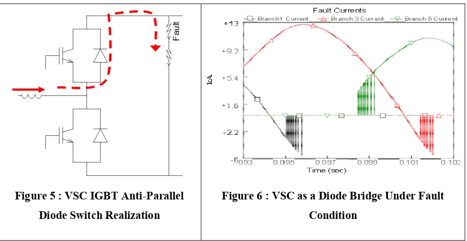
This current is limited only by the input inductor impedance, thereby causing currents as high as 13kA through a device that is rated to handle only about 4kA.
F
au
lt
Figure 5 : VSC IGBT Anti-Parallel Diode Switch Realization
kA
Figure 6 : VSC as a Diode Bridge Under Fault Condition
Some method to extinguish the DC fault is necessary. One of the methods is to use an AC circuit breaker on the AC side of the voltage source converter (VSC) or another method is to use a solid state hybrid FCLCB as discussed earlier.
All these methods require action by devices external to the PEBB to interrupt and isolate the fault. This section investigates the proposal of utilizing the PEBB themselves for interrupting the DC faults.
Similar to the FCLCB discussed above which uses positive temperature coefficient resistor in a hybrid concept for fault current limiting and breaking, semiconductor devices (like MOSFET, IGBT, ETO, etc) also have highly non-linear resistance characteristics in their active region. The operation of semiconductor devices in the active region (by gate voltage control) has been discussed in literature [4, 24, 25] as a useful technique for handling short circuits and for dv/dt control.
fault current. Again, segregation based on elapsed time is used to differentiate the transient faults from sustained faults. For sustained faults, the gate voltage of the device is reduced until the device is completely turned-off, thereby achieving a complete shut-down in a controlled manner. This technique, known as soft shut-down, has been effectively used to extend the short circuit withstand time of devices possessing Forward Biased Safe Operating Area (FBSOA), such as the power MOSFET, IGBT and ETO.
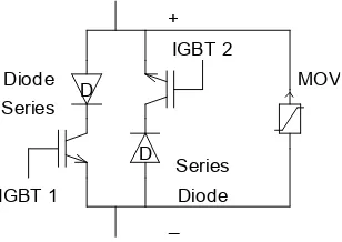
As discussed, the conventional PEBBs require external devices like ACCB/fuses and/or crowbar protection for interruption and isolation of fault. Therefore, to eliminate this requirement, it is desirable to modify the topology of a conventional rectifier such that the fault can be interrupted by itself and eliminate the external devices that are required to interrupt the fault. To do so, we replace the anti-parallel diode of Figure 5 with a controllable semiconductor device (CSD), so that under fault condition, the CSD would not free wheel.
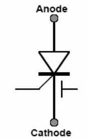
Two options – IGBT and ETO, were considered for replacing the diode with a CSD. The study in [19] considered one of the options to replace the anti-parallel diode from switch realization of a conventional rectifier bridge by an anti-parallel IGBT, to obtain the switch realization as shown in Figure 7.
D
_ D
+ IGBT 2
Series Diode Series
Diode MOV
IGBT 1
Figure 7 : Bi-Directional Current Control Switch Realization
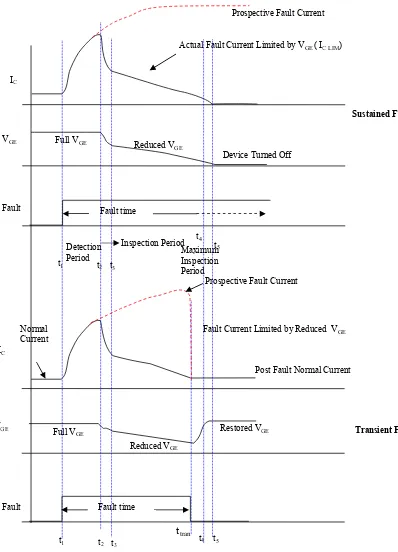
Figure 8 : Fault Handling by Operating Switch in Saturation Region
Analysis was also done to determine voltage stresses on the devices of the bridge under normal and fault conditions and under device saturation. It was found that properly chosen
Actual Fault Current Limited by VGE ( IC LIM)
IC IC
Prospective Fault Current
Fault VGE
VGE
Fault
Sustained Fault
Transient Fault
Full VGE
Reduced VGE
Restored VGE
Post Fault Normal Current Fault Current Limited by Reduced VGE
Fault time
Prospective Fault Current
Detection
Period Maximum Inspection Period Full VGE Reduced VGE
Device Turned Off
t1 t2 t3
t4 t5 Fault time
t1 t2 t3 t4 t5 ttran
Inspection Period
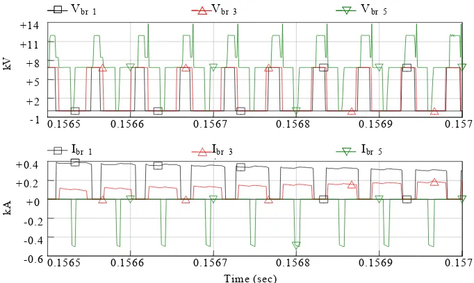
devices could withstand the stresses under fault and successfully turn-off by interrupting the fault current. Figure 9 shows voltage and current stresses on the power electronic devices of a rectifier when operating in saturation / active region during turn-off.
0.1565 0.1566 0.1567 0.1568 0.1569 0.157
-1 +2 +5 +8 +11 +14
Vbr 1
0.1565 0.1566 0.1567 0.1568 0.1569 0.157
-0.6 -0.4 -0.2 +0 +0.2
+0.4 Arm 3 Current
kV
kA
Vbr_3 Vbr_5
Ibr 1 Ibr 3 Ibr 5
Time (sec)
Figure 9 : Voltage and Current Stress under High Impedance Fault
By replacing the diodes by IGBTs, we have many advantages [19]. On the other hand the disadvantages of IGBT which weigh in heavily, in favor of ETOs:
(1) The IGBTs are relatively less robust as compared to ETOs. This demands that VERY fast fault detection circuits be used for IGBTs and this also requires a fast initiation of turn-off (order of few Is),
(2) Single IGBTs do not have high voltage high current withstand capability, thus requiring many series and parallel devices to achieve the required voltage and current ratings respectively and
(3) Higher numbers of isolated power supplies are necessary for IGBT gate control.
shows the circuit symbol of an ETO [16, 26].
Figure 10 : Equivalent Circuit of ETO Figure 11 : ETO Circuit Symbol
The ETO has many desirable features. Theoretical analysis and experimental results suggest that the ETO has the combined advantages of both the GTO and the IGBT, namely, GTO’s high voltage and current rating, low forward voltage drop, and IGBT’s voltage control, high switching speed, wider RBSOA, high reliability [26]. Its ability to turn off high currents while simultaneously sustaining the high voltage, gives it a robust Reverse Biased Safe Operating Area (RBSOA). The ETO thyristor also has another important feature of having a series MOSFET in the cathode terminal (emitter terminal) which is used for current sensing through the device. This current sensing can be very effectively used for turning off the device before the maximum controllable current limit is reached. This feature is used for the Switch Level Autonomous Protection, as will be described later. The operation of the semiconductor device (ETO or IGBT) in the active region has been discussed in literature [4, 24, 25, 27] as a useful technique for handling short circuits and for dv/dt control, as shown above in Figure 8.
A
Figure 12 : ETO Snubberless Turn-Off Capability
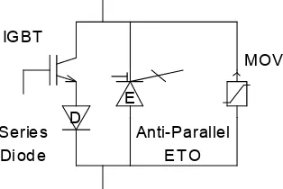
For our application, where the ETO would replace the diode, the switching requirements on the ETO are quite lenient. Under normal operation of the VSC, the ETO is fired continuously to emulate a diode operation (i.e. when a positive voltage is applied across it, it is fired ON, and hence conducts, else not). Thus, the operating principle of the VSC is not modified. This new switch realization is shown in Figure 13.
D E
MOV
Anti-Parallel ET O Serie s
Diod e IGBT
Figure 13 : Switch Realization with IGBT and Anti-Parallel ETO Device
6 2 4
F6 F2 F4
1 F3 3 5
F1 E E
E
F5
G F G F G F
G F G F G F
E E
Cref Bref
E
I Br_
1
I Br_
3
I Br_
5
I Br_
6
V
br_ 3
V
br_1
I Br_
2
I Br_
4 V br_5 C o + -V R I out s L s L s L Aref I_C I_B I_A
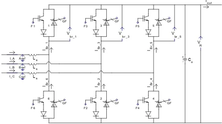
Figure 14 : Modified Rectifier PEBB Topology
Simulations were performed in PSCAD/EMTDC to demonstrate the fault interruption capability of the modified rectifier PEBB. A non-linear switching model was designed in PSCAD by the author to properly represent the current limiting and soft turn-off of the ETOs in the active region during gate controlled ETO shutdown. The simulation results demonstrating the fault current interruption by the rectifier are shown in Figure 15 and Figure 16. Figure 15(a) shows the DC Bus voltage VR. Figure 15(b) and (c) show the six branch
currents IBr1, IBr2,… IBr6. Figure 15(d) shows the three branch voltages VBr1, VBr3 and VBr5.
Figure 16 shows the rectifier input currents Ia, Ib and Ic.
0.059 < t < tfault: Normal Operation : The DC bus voltage is at the normal rated value of 7kV. The branch currents under normal PWM switching are the rated value of 650A (peak). When a branch is “OFF”, VRis applied across the branch and when a branch is “ON” the
on-state voltage appears across it. This is represented by VBr1, VBr3 and VBr5 in Figure 15(d).
tfault < t < tsoftoff : Faulted Condition : At tfault = 0.06s, a fault occurs at the output terminals
of the rectifier. VR collapses to a very low value determined by fault impedance.
the increasing fault current, and the VSC starts operating in a diode bridge rectifier mode.
tsoftoff < t < tshutdown : Soft Turn-Off : At tsoftoff =0.06095s, it is established, based on time
segregation, that a sustained fault has occurred. Also, the current IBr3 approaches the device
maximum turn-off limit of 3kA, and a “soft turn-off” or gradual ramping down of the gate voltages of all the devices is initiated. The ramping down of the gate voltages results in the ramping down of the currents IBr3 IBr4… IBr6. This current ramping causes the voltages VBr1,
VBr3 and VBr5 to rise. This voltage rise is limited by the MOV to 14kV. The whole soft
turn-off process is finished within about 20 µsec, but the shut-down is not complete as the rectifier input current (also the generator current Figure 16) has not been interrupted. The MOVs free-wheel the current until tshutdown.
tshutdown < t < 0.0615: Shut down : At tshutdown = 0.6125 the freewheeling action of the
MOVs ceases and the fault current is completely interrupted by the PEBB. The full line voltage is applied across the branches as represented by the voltages VBr1, VBr3 and VBr5. The
application of the nominal voltages across the branches causes the MOVs to go back into non-conducting state.
The generator currents which constitute of the branch current (or the rectifier input current) is shown in Figure 16. At t = 0.06s, the fault causes the current to rise till the soft shutdown of the rectifier is initiated at tsoftoff = 0.06095s. The current is interrupted in a controlled manner
to completely shutdown the rectifier PEBB.
T im e ( s e c )
(a )
0 . 0 5 9 0 .0 5 9 5 0 .0 6 0 .0 6 0 5 0 .0 6 1 0 . 06 1 5
k
V
+ 0 + 1 .6 + 3 .2 + 4 .8 + 6 .4
+ 8 V _ R
(b )
0 . 0 5 9 0 .0 5 9 5 0 .0 6 0 .0 6 0 5 0 .0 6 1 0 . 06 1 5
k
A
- 0 .8 - 0 .0 8 + 0 .6 4 + 1 .3 6 + 2 .0 8
+ 2 .8 I B r 1 I B r 3 I B r 5
(c )
0 . 0 5 9 0 .0 5 9 5 0 .0 6 0 .0 6 0 5 0 .0 6 1 0 . 06 1 5
k
A
- 0 .8 - 0 .2 2 + 0 .3 6 + 0 .9 4 + 1 .5 2
+ 2 .1 I B r 6 I B r 2 I B r 4
(d )
0 . 0 5 9 0 .0 5 9 5 0 .0 6 0 .0 6 0 5 0 .0 6 1 0 . 06 1 5
k
V
-1 4 - 8 .4 - 2 .8 + 2 .8 + 8 .4
+ 1 4 V _ B r_ 1 V _ B r _ 3 V _ B r _ 5
tshutdown
tsoftoff tfault
Figure 15 : Rectifier Shutdown
Time (sec)
0.0425 0.0475 0.0525 0.0575 0.0625
kA -2.1 -1.12 -0.14 +0.84 +1.82
+2.8 I_A I_B I_C
(a) Generator Currents
Time (sec)
0.0595 0.06 0.0605 0.061 0.0615
kA -2.1 -1.12 -0.14 +0.84 +1.82
+2.8 I_A I_B I_C
Soft turnoff
Fault Shut Down
(b) Zoom-in of (a)
2.5 Inverter Fault Current Limiting CB
Inverters are used to feed AC motor loads and other electronic loads. They are also used in high power applications in conjunction with rectifiers for transmission purposes. Another application of inverters is in conjunction with fuel cells which give DC as output. In all these applications the inverters employ PWM. Simulations using PSCAD/EMTP were performed on a test system. A 3-phase inverter as shown in Figure 17 is connected to an ideal DC source and a 3 phase squirrel cage induction motor, is used in our simulation.
Simulation results for an inverter PEBB show that the diodes in an inverter do not free-wheel indefinitely under fault at the output terminals of the inverter. A turn-off signal to all the gate controlled devices of the inverter PEBB is effective way to interrupt the fault current and isolate the fault. This indicates that the topological modifications that were necessary in case of a rectifier PEBB for interruption of fault are not necessary for an inverter PEBB. And, therefore, a conventional inverter PEBB can be used for circuit breaking function without modification to the topology. For such an inverter to act as a circuit breaker under fault condition, it is just necessary to turn-off all the controllable devices in the bridge.
V ETO5 V ETO3 V ETO1
V ETO6 V ETO2
1
5 3
6
4 2
v4
L
C +
- C
+
C +
Iin
Vd
L L
a
b
c
Id5 Id3 Id1
Id6 Id2
Id4
Ic
Ia
Ib
-
-V ETO4
Vca
Vab
Vbc
IETO6 IETO2
IETO4
IETO1 IETO3
IETO5
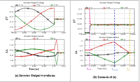
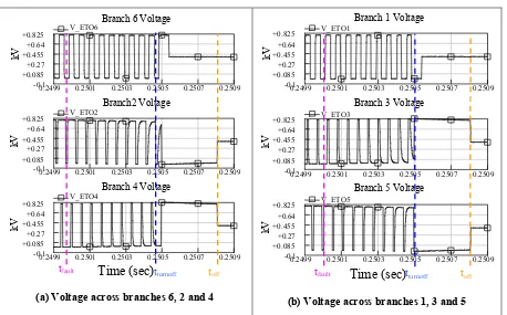
Modern inverters employ IGBT (for high switching frequency, medium power applications) or GTOs (for lower switching frequency, high power applications) as the controllable semiconductor devices. Although the use of any gate controllable device (GTO, IGBT, ETO etc) for switch realization, allows the inverter PEBB to be used as a circuit breaker, in our simulations ETOs have been used to allow for longer withstand times along with high switching frequency, higher breakdown voltages at high power levels. Simulation results are shown in Figure 18, Figure 19, Figure 20 and Figure 21. Figure 18(a) shows the inverter output voltages, Vab, Vbc and Vca and inverter output currents, Ia, Ib and Ic. Figure 18(b)
shows the zoom-in of the Figure 18(a) around the fault occurrence. The device currents of the six branches are shown in Figure 19 and the six branch voltages are shown in Figure 20. The inverter input current Iin is shown in Figure 21.
0.2500 < t < tfault : Normal Operation : The inverter output voltage Vab, Vbc and Vca and the
inverter full load output line currents Ia, Ib, and Ic are at the nominal values of 450 V (L-L
peak) and 700A (peak) respectively. When a branch is “OFF”, the corresponding voltages VETO1, VETO2, …, VETO6 are the normal input DC value of 800V while when the branch is
“ON” the voltages VETO1, VETO2, …, VETO6 are normal forward voltage drop of the CSDs. Iin
represents the normal charging-discharging current of the inverter PEBB.
tfault < t < <tturnoff : Faulted condition : A fault at tfault = 0.2500s causes the voltage Vab, Vbc,
Vca to collapse and the line currents to Ia, Ib, and Ic to rise. The fault causes only a minor
change in the voltages VETO1, VETO2, …, VETO6. The Iin starts increasing proportional to the
increase in the output current due to the inverter output 3 phase fault currents.
tturnoff < t < toff : Diode freewheeling : At tturnoff = 0.2505s, enough time has passed to rule
out a temporary transient fault establishing a sustained fault. In addition, since the currents are approaching the device limits, gating to the CSDs of the inverter PEBB is stopped. Turning off the CSDs at tturnoff = 0.2505s limits the current from increasing further and
initiates the shutdown of the PEBB. The currents Ia, Ib, and Ic are not “chopped” off, but
inductors, and returning through the diode of branch 1 and ETO of branch 4.
At tturnoff = 0.2505s, when the CSDs are gated off, to maintain the continuity of the current
through the output inductor of phase b, the current flowing through the ETO of branch 3 is commutated into the diode of branch 2. Similarly, to maintain the continuity of the current through inductor of phase c, the current flowing through the ETO of branch 4 is commutated into the diode of branch 5. The diode of branch 1 which was conducting prior to tturnoff
continues to conduct till current zero of phase a thereby maintaining the continuity of the current through the inductor of phase a. The commutation of the currents from the ETOs into the diodes causes the Iin to reverse, that is, to reverse feed into the source as seen by the
negative current in Figure 21 after tturnoff. The energy stored in the inductor is completely fed
back to the source and the shutdown of the PEBB is complete at toff = 0.2508s.
toff < t < 0.2509 : At toff=0.2508s the shutdown is complete. The currents Ia, Ib, and Ic are
interrupted and the post fault voltage is shared equally (=0.4kV) among the top (1, 3 and 5) and bottom (6, 2 and 4) branches as seen in Figure 20. At toff, the PEBB has successfully
interrupted the current.
Time (sec)
Inverter Output Voltage
0.242 0.244 0.246 0.248 0.25 0.252 -0.6
-0.36 -0.12 +0.12 +0.36
+0.6 V ca V bc V ab
Inverter Output current
0.242 0.244 0.246 0.248 0.25 0.252 -2.5
-1.46 -0.42 +0.62 +1.66
+2.7 Ia Ib Ic
kV
kA
(a) Inverter Output waveforms
Time (sec)
Inverter Output Voltage
0.2499 0.2501 0.2503 0.2505 0.2507 0.2509 -0.27
-0.114 +0.042 +0.198 +0.354
+0.51 V ca V bc V ab
Inverter Output current
0.2499-3 0.2501 0.2503 0.2505 0.2507 0.2509 -1.8
-0.6 +0.6 +1.8
+3 Ia Ib Ic
kV
kA
tfault tturnoff toff
(b) Zoom-in of (a)
Time (sec) Branch 6 Currents
0.2499 0.2501 0.2503 0.2505 0.2507 0.2509
-0.01 +0.13 +0.27 +0.41 +0.55
+0.69 I_ETO6 Id6
Branch 2 Currents
0.2499 0.2501 0.2503 0.2505 0.2507 0.2509
-0.1 +0.46 +1.02 +1.58 +2.14
+2.7 I_ETO2 Id2
Branch 4 Currents
0.2499 0.2501 0.2503 0.2505 0.2507 0.2509
-0.1 +0.42 +0.94 +1.46 +1.98
+2.5 I_ETO4 Id4
tfault tturnoff toff
kA
kA
kA
(a) Currents of Branches 6, 2 and 4
Time (sec)
Branch 1 Currents
0.2499 0.2501 0.2503 0.2505 0.2507 0.2509 -0.01
+0.128 +0.266 +0.404 +0.542
+0.68 I_ETO1 Id1
Branch 3 Currents
0.2499 0.2501 0.2503 0.2505 0.2507 0.2509 -0.1
+0.46 +1.02 +1.58 +2.14
+2.7 I_ETO3 Id3
Branch 5 Currents
0.2499 0.2501 0.2503 0.2505 0.2507 0.2509 -0.1
+0.42 +0.94 +1.46 +1.98
+2.5 I_ETO5 Id5
kA
kA
kA
tfault tturnoff toff
(b) Currents of Branches 1, 3 and 5
Figure 19 : ETO and Diode Currents
Time (sec)
Branch 6 Voltage
0.2499 0.2501 0.2503 0.2505 0.2507 0.2509 -0.1 +0.085 +0.27 +0.455 +0.64 +0.825 V_ETO6 Branch2 Voltage
0.2499 0.2501 0.2503 0.2505 0.2507 0.2509 -0.1 +0.085 +0.27 +0.455 +0.64 +0.825 V_ETO2
Branch 4 Voltage
0.2499 0.2501 0.2503 0.2505 0.2507 0.2509 -0.1 +0.085 +0.27 +0.455 +0.64 +0.825 V_ETO4 kV kV kV
tfault tturnoff toff
(a) Voltage across branches 6, 2 and 4
Time (sec)
Branch 1 Voltage
0.2499 0.2501 0.2503 0.2505 0.2507 0.2509 -0.1 +0.085 +0.27 +0.455 +0.64 +0.825 V_ETO1
Branch 3 Voltage
0.2499 0.2501 0.2503 0.2505 0.2507 0.2509 -0.1 +0.085 +0.27 +0.455 +0.64 +0.825 V_ETO3
Branch 5 Voltage
0.2499 0.2501 0.2503 0.2505 0.2507 0.2509 -0.1 +0.085 +0.27 +0.455 +0.64 +0.825 V_ETO5 kV kV kV
tfault tturnoff toff
(b) Voltage across branches 1, 3 and 5
Time (sec)
0.2498 0.25 0.2502 0.2505 0.2507 0.2509
-2.7 -1.62 -0.54 +0.54 +1.62
+2.7 I in
tfault tturnoff toff
kA
Figure 21 : Inverter Input Current
The limiting and interruption of the fault current has been achieved by turning off the controllable devices in the inverter (before they reach their limits). The freewheeling of the diodes allows the current to decay to zero and prevents any over-voltages in the PEBB. The PEBB withstands the high fault currents for 0.5ms and limits the fault current for another 0.3ms before the inverter is completely shuts down. This gives time for the overall system protection scheme to differentiate transient and sustained fault and act accordingly.
Summarizing, a conventional inverter PEBB can withstand a fault and turn off to interrupt the fault current without causing damaging over voltages, thereby functioning successfully as a current limiting circuit breaking PEBB.
2.6 Buck Converter Fault Current Limiting CB
A typical full bridge buck converter along with its associated filters is shown in Figure 22.
Sw1
Sw2 Sw3
Sw4
#1 #2
Iin
L2 L
o
Io
Cin
+
- +- Co
L1
5:1
BCIS
Vin
BCRS
Buck Converter Inverter Stage
Buck Converter Rectifier Stage
Vo
D
D
D
D
Note that the Buck converter has an inverter stage (BCIS) connected to the rectifier stage by an isolation transformer. By adopting a proper PWM, we can have the switches of this stage to carry only unidirectional currents [29]. This will allow us to realize the switches of the BCIS by ETOs without anti-parallel diodes and thus, we can turn the Buck converter completely off by turning off all the switches of BCIS. The modified topology with this switch realization is shown in Figure 23.
1
2 3
4
Iin
L2
Lo
Io
Cin
+
- +- C0
L1
5 : 1
i1 i3
i2 i4
v1 v3
v4 v2
Buck Converter Inverter Stage Buck ConverterRectifier Stage
Figure 23 : Modified Full Bridge Buck Converter
With this modified switch realization, we can use the BCIS to interrupt the faults by employing the same technique (hard turn-off) as employed above for the inverter. The main concern here is the voltage stress by chopping (due to absence of freewheeling diodes) of the current through the input inductor L2 and the transformer magnetizing current. However
since the associated input inductor, L2 is very small, less than a IH, the voltage stress is
negligible, given that the device turn-off time is about 3-5Is. Also, turning off all the switches in the BCIS will force the transformer magnetizing current to flow through the secondary winding and therefore the current will not be chopped and does not result in any extra voltage stress on the devices. Therefore, the turn-off operation of a buck converter under fault can be done similar to the turn-off of the inverter PEBB.
To test the current limiting of the buck converter with the proposed scheme, the buck converter of Figure 23 was simulated, which employs ETOs as the CSDs. The converter is supplied from a DC source of 7kV and steps down the voltage to 800V DC. A short circuit at the output DC terminals is created for the simulation. The branch currents i1, i2, i3and i4and
0.0492 < t< tfault: Normal Operation : Under normal operation of the buck converter, the full
load rated current flows through the ON devices i1 and i2 or i3 and i4. Figure 25 shows the
voltages v1,v2,v3and v4. The voltages across an ETO are at a value of 3.5kV, when the both
the ETOs of a leg are OFF, for example, when ETO1 and ETO4 are OFF, they share the voltage and v1and v4are at a value of 3.5kV. Whereas, when only one of the ETOs of the leg
is OFF the voltage across it is 7kV. For example, when ETO1 is ON, ETO4 is OFF; therefore voltage across ETO1, v1, is the low forward voltage drop, while the voltage across the OFF
ETO4, v4is 7kV.
tfault < t < toff : Faulted Operation : A fault occurring at t = 0.05s forces the current through
the CSDs to rise to W3kA in 900Is after fault. At this time, a transient fault is ruled out based on time segregation and the current approaches current limits of the CSDs.
toff < t < 0.0512 Shutdown :At toff = 0.0509s, the gating signals to the BCIS are stopped and
the BCIS is completely turned-off. The currents i1, i2, i3 and i4 cease to flow. The
un-availability of a current path for the magnetizing current on the primary side of the isolating transformer forces it through the secondary winding of the transformer. The diodes of the BCRS free-wheel the current though the output capacitor, the short circuit and load. After the turn-off, the input voltage of 7kV is shared equally (3.5kV each) among top and bottom CSDs.
Thus, we see that a properly controlled buck converter can limit and interrupt a fault in less than 1ms. In addition; it can limit and interrupt the fault current without excessive voltage stress on the switches
The pulsed capacitor currents which flow through the branches constitute the transformer input currents. Following the fault, currents 6x the rated currents flow through the transformer for a few hundred Is, this causes simultaneous high current and rated voltage in the transformer, for short period. The transformer should be properly chosen for such a duty. The considerations for selection of a proper transformer are given in Appendix B.
perform the functions of a current limiting circuit breaker.
Time (s)
0.0492 0.0496 0.05 0.0504 0.0508 0.0512
+0 +0.62 +1.24 +1.86 +2.48
+3.1 i1 i3
0.0492 0.0496 0.05 0.0504 0.0508 0.0512
+0 +0.7 +1.4 +2.1 +2.8
+3.5 i4 i2
kA
kA
tfault toff
(a)
(b )
0.051 6
0.0516
Figure 24 : Branch (ETO) Currents
Time (sec)
0.0492 0.0496 0.05 0.0504 0.0508 0.0512 -0.25
+1.25 +2.75 +4.25 +5.75 +7.25
v1 v3
0.0492 0.0496 0.05 0.0504 0.0508 0.0512
-0.25 +1.25 +2.75 +4.25 +5.75 +7.25
v4 v2
kV
kV
toff
tfault
Figure 25 : Voltage across Branches (ETO)
2.7 Chapter Summary
3 DC DISTRIBUTION SYSTEM PROTECTION
3.1 Introduction and Overview
In AC systems, all the devices of the system (generators, transformers, lines etc) are covered by one or more protection schemes (overlapping zones). The important devices have their own protections called the unit protections, which trip if and only if the fault is in their zone of protection, namely in the device. Therefore, these protection schemes are device based, i.e., they are aimed to protect the devices etc, on a system.
In the new DC SES, the PEBBs, which are expensive devices, would also need unit protection. In the envisioned protection scheme for the SES, the PEBBs are also used as fast acting current limiting circuit breakers. With this new functionality for the PEBBs, a new challenge emerges, that the protection scheme should be also able to detect and locate the faults faster. To achieve this goal, an "agent" based system protection in contrast to the conventional protection scheme has been designed here, which consists of smart agents embedded into the PEBB. The "Protection-Agents" of this new Agent based System Protection will monitor only the local quantities to detect and isolate the disturbances. This local protective action will ensure that protection actions are very fast which aid to reduce the system downtime.
The agents will perform two primary tasks: system protection for detecting and isolating disturbances and reconfiguration management to provide service continuity to the part of the network that is undamaged. This chapter deals with the first task.
3.2 Conventional HVDC Protection: Literature Survey
ACCB
Figure 26 : Typical Configuration of a Bipole Converter Station
Different types of faults can occur on the bipole converter stations. These faults can occur on the supply line, the converter transformer, the converter or on the dc side. The protections provided to protect against these faults, are divided into AC protections and DC protections. The protective action to interrupt and isolate these AC or DC faults is to open the AC circuit breaker. Even for faults on the DC Line, due to the absence of a DC circuit breaker, the ACCB has to open to interrupt the fault current and isolate the fault.
The AC side protection is provided to the AC line which feeds the AC supply bus, the AC supply bus, and the converter transformer.
The DC protection is divided into valve protections and DC side protection. Of these, the protections that are most relevant to PEBB protections are the valve short circuit protection, converter over-current protection, valve misfire (shoot-through), voltage stress protection, converter DC differential protection, and DC over-voltage protection.
(1) Valve short circuit protection: The objective of the protection is to detect short circuits across the valves of the converter. The shorts are cleared by blocking the converter firing and tripping the AC side circuit breaker.
(3) Valve misfire protection: The valve misfire protection detects the failure of a valve to conduct when a control pulse has been applied, detect unintentional valve firing. It also performs two additional functions to prevent the selection of a valve as a bypass valve, if the valve has failed, and to select the valve as a bypass valve, if the valve is firing unintentionally. The protective action is to transfer control to the redundant control system, block the converter and trip the AC side circuit breaker.
(4) Voltage stress protection: The objectives of voltage stress protection are two-fold. First, it is designed to detect high commutation voltages and to prevent further increase of voltage by interlocking the converter transformer tap changers. Second, it takes the faulty converter out of service in the case of persistent AC over-voltage. On detection of a small over-voltage, the tap-changers are inhibited from further raising the voltage. On detection of a high over-voltage, the converter is blocked and the AC circuit breaker is tripped.
(5) Converter DC differential protection: The objective of this protection is to detect ground faults on the DC side of the converter between the transducer in the DC wall bushing on the low voltage terminal and the transducer in the DC reactor on the line side, Figure 26. The protective action is to block the converter, trip the AC side circuit breaker and isolate the pole and the line at both ends.
(6) DC over-voltage protection: The objective of this protection is to detect over-voltage on the DC line and equipment when starting a pole against an open-ended DC line. The protective action is to transfer control to the redundant control system, block the converter and isolate the pole and the line at both the ends.
3.3 PEBB Based DC SES Protection
functionally for PEBB can be achieved by proper selection of converter topology and by adopting a revised switch realization that uses the newly emerging robust power electronic devices such as ETO [26, 30-32].
The following sections explain the developed system protection scheme for the DC SES. The new protection scheme is designed to be hierarchical in nature so that the backup protection for the failure of the primary protection can be very fast and automatic. At the top of the hierarchy is the primary protection called the Agent Based System Protection and at the bottom level of the hierarchy is the backup protection called the Switch Level Autonomous Protection. A schematic of the protection scheme for the DC SES is shown in Figure 27.
Figure 27 : Hierarchical Protection for the DC SES
3.4 Switch Level Autonomous Protection
At the lowest level of the hierarchy, the protection is provided to the basic switching element - the ETOs. Protection in this Tier is Switch Level Autonomous Protection (SLAP) which means that it does not interact with the system protection to initiate protective action. The aim of the SLAP is to work independently/autonomously and protect the individual switches from destruction. This is also the last line of protection for the CSD, and therefore defines the ultimate limits that the switch can be operated at. Therefore, the system protection must be faster than this protection and must be coordinated with it such that the system protection operates before the SLAP operates.
This type of protection (SLAP) can be either embedded into the switch (by customized Agent Based System Protection
Switch Level Autonomous Protection (SLAP)
PEBBs
Rectifier, Buck Converter & Inverter Agent
Capacitors CDCCB
Bottom TIER (Backup)
S
eq
ue
nc
e
of
O
pe
ra
ti
on
manufacturing) or external means can be provided. For this study we would use embedded means (explained below) for protection of the ETO switch in the SES.
Figure 28 shows the ETO’s embedded gate drive circuit which is used as Switch Level Autonomous Protection in this protection scheme [16]. The voltage across QE, VQE, is
proportional to the current through the device. This VQE is first filtered by Rf and Cf and is
then sent to the analog comparator to be compared with the reference voltage Vref, which
represents the setting current for turn-off. Once the VQE is larger than Vref, indicating the
device current is higher than the setting current, the comparator will change its output from high logic level to low logic level. After a delay (about 3µs) dictated by Rdand Cdto prevent
the false trigger, the signal Vout changes its state. The Vout is ANDed with the normal PWM
firing signal of the controller and the output is appropriately connected to the gate of the ETO (gates of QE and QGas shown in Figure 28. When Vout goes low, the ETO device is turned
off to cut off the fault current within 3µs, as experimentally shown in Figure 29.
Figure 28 : ETO Gate Drive Circuit for Over-Current Protection
3.5 Agent Based System Protection
At the top level of the hierarchy of the protection scheme for the DC SES is the Agent Based System protection as shown in Figure 27. The basic task is the same as any other protection scheme for a power system - locate any disturbance that can occur on the system and take appropriate action in order to minimize the effect of disturbance on the operation of the system. The aim here is to design a very effective protection scheme which is able to locate the disturbance and isolate the affected area very quickly. It should also keep the isolated area as small as possible. We plan to make use of the special features of the DC SES to achieve this goal.
Figure 30 : DC SES with Circuit Breakers
For the new PEBB based DC distribution system, it has been shown that we can use the PEBBs themselves to perform CB duties, and thus, eliminate the need for separate CBs for protection. Therefore, the CBs will be embedded within the PEBBs and the protection zones that will be defined by them will not be device based. The SLAP, as described above will provide backup protection. Figure 31 illustrates the main zones defined by these devices on the prototype DC SES. Note that there will be three main zones:
• Primary DC Bus Zone: The primary DC bus supplies power to all the load zones and therefore it is the most critical component for protection. It is also the one that is exposed the most to the faults / damages. Note that since the switches in the PEBBs will be doing the fault interruption, therefore the protection zone is defined by the switches of PEBBs that are connected to the bus – the rectifiers, and the buck converters. The zone therefore includes not only the bus but also the DC rail of the rectifiers and the buck converters, as the figure illustrates. Note that, to protect the DC bus only using conventional schemes; we would need a CB at every connection point, as illustrated in Figure 30. The proposed scheme eliminates these CBs.
AC Load
G1 G2
Rectifier
Buck Converter
DC Load
Inverter
CB
• Secondary DC Bus Zone: The secondary DC bus supplies power to all the loads within a given zone either directly to the DC loads or via inverters to AC loads. Therefore the secondary DC bus is the second most critical component for protection. Different load zones on a ship are typically separated by watertight bulkhead compartments of the ship and therefore the faults occurring in a load zone is localized to that zone. One load zone is illustrated in Figure 31; it is defined by the buck converter and includes the secondary DC bus, the load side buck converter rails and the source side inverter rails.
• Rectifier AC Zone: As Figure 31 illustrates, the rectifiers are connected to the AC source bus supplied by generators. Note that the part of AC source side of the rectifier which includes the rectifier input filter elements need to be protected, and the rectifier switches cannot be used for this purpose. As the figure illustrates, we propose to use fuses at the source terminals of the rectifier to protect this AC source side of the rectifiers. Note that the generators have usually their own protection zones defined by their CBs as illustrated in the figure.
Figure 31 : Zones of a DC SES
Yellow
Green Pink Blue
Pink
Blue
Pi
nk
Red Rectifier AC Zone
Primary DC Bus Zone
Secondary DC Zone
Rectifier AC Zone
G1
Load Zone Source Side DC
Rail of Buck
Converter
Source Side
+DC Rail of
Buck Converter
Source Side +DC Rail of Inverter
DC Rail of Rectifier
AC Source Bus 2 AC
Source Bus 1
Fuse
G2
+ DC Rail of Rectifier DC Bus interface
Diode
Load Side DC
Rail of Buck
Converter Load Side +DC
Rail of Buck Converter Gen Breaker
AC Load
Pi