A Single-Phase Ac-Dc Converter with
Improved Efficiency Using Atmega8
Microcontroller
Bhuvaneswari.K1, Niruba. K2
PG Scholar (PSE), Dept. of EEE, V.S.B. Engineering College, Karur, Tamilnadu, India 1
Assistant Professor, Dept. of EEE, V.S.B. Engineering College, Karur, Tamilnadu, India 2
ABSTRACT: This paper proposed an AC-DC semi-bridgeless boost converter with 180 degree phase shift and less number of switches. The simplified current sensing method is applied in the converter to predict the inductor. The proposed converter has the advantageous features such as high efficiency at light loads and low ac input lines; compact in size, less charging time, and less amount and cost of electricity drawn. This project presented simulation results of a boost converter, converting the 230V ac input voltage to 400 V dc at upto 3kW Load. The power factor of the proposed system is maintained above 0.9 and the THD level is below 5%. The converter can works with less EMI. This type of converters is used for vehicle charging and residential charging application. The ATMEGA8 micro controller is for the controlling process, which has fast response with RISC architecture.
With solar source the semi bridgeless converter can acts as the dc-dc boost converter.
Keywords: AC–DC converter, boost converter, DC-DC converter, Bridgeless power factor correction (PFC), current sensing, plug in charger.
I.INTRODUCTION
A storage system that can be recharged by connecting a plug to an external electric power source. The charging AC outlet predictably needs a plug in AC/DC charger with a power factor correction. For the PFC application a multiple of circuit topologies and control methods have been developed.
The single-phase active PFC techniques can be classified into two approaches: they are single-stage approach and the two-stage approach. The single-stage approach is right for low power level applications. It can only apply for lead acid batteries charging because of frequency ripple problem. Therefore, the two-stage approach is the most suitable for high storage battery chargers used for high power applications, where the power rating is relatively high, and lithium-ion batteries are used as the main energy storage system. In the two-stage architecture, the first stage is PFC rectification where it rectifies the input ac voltage and transfers it to a dc-link. At the same time, the PFC is also achieved. A phase shifted semi bridgeless PFC topology operated under continuous conduction mode as the two stage charger specifically with the ac–dc PFC converter and dc-dc converter for battery charging with various duty cycles.
A .Interleaved PFC boost topology
This boost topology uses two boost converters in parallel operating 180° out of phase [1]–[3] by switching 180° out of phase, it doubles the effective switching frequency and introduces a smaller input current ripple; thus, the input electromagnetic interference (EMI) filter can be smaller than a single PFC boost topology [4]–[6].The drawback of this topology is the very high loss and the resultant heat management issue for the input diode bridge rectifiers.
B. Bridgeless PFC boost topology
topology [17]. The Drawback of this topology is the floating input line with respect to the PFC stage ground, which makes it impossible to sense the input voltage without a low-frequency transformer or an optical coupler.
C. Dual-boost PFC topology
The advantage of dual-boost PFC topology is [18] minimizes the gate loss, reduces the losses at light loads, the conduction loss can be minimized. The light-load efficiency , improved by an external device, which leads cost expense and improve controller complexity.
D. Semi-bridgeless PFC boost topology
Semi-bridgeless PFC boost topology is the conventional bridgeless topology with two extra slow diodes, that is, Da and Db that connect the input to the PFC ground. The slow diodes were added to address EMI- related issues [15],[16].The current does not return through these diodes; therefore, their related conduction victims are small. The semi-bridgeless configuration also resolves the suspended input line problem with respect to the PFC stage ground.
E. Current sensing techniques
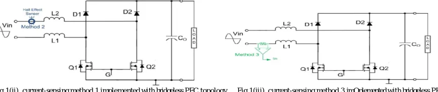
Three exclusive current-sensing circuits (Methods 1–3) for the bridgeless PFC boost topology are shown in Fig. 4 to sense the current in the MOSFET and diode paths independently, as the current path does not share the similar ground throughout each half-line cycle [7], [19].
Method 1 Fig. 1 (i) is the passive current-sensing scheme reported in [7], which requires three current-sensing transformers, one in series with each switch and a third in the positive dc rail to sense the collective current of the two diodes, and a supplementary signal transistor with its related difficult control circuitry.
Method 2 Fig.1 (ii) uses a simple, but the costly Hall Effect sensor to straightly sense the input current.
F i g . 1 ( i ) . current-sensing method.1 implemented with bridgeless PFC topology.
Fig 1(ii). current-sensing method.1 implemented with bridgeless PFC topology. Fig 1(iii). current-sensing method.3 imQplemented with bridgeless PFC topology.
Method 3 Fig.1(iii). uses a differential-mode amplifier, which is connected in series with the input. This method is moderately less cost.
II-PROPOSED SYSTEM
Vehicle storage charging is one of the applications of PSSB converter [22]. The Fig. 2. represents the block diagram of Phase Shifted boost power factor corrected converter.
PSSB BOOST CONVERTER
Fig.2. PSSB-block diagram Fig. 3. Proposed PSSB PFC boost topology with the current-sensing circuit
The proposed PSSB topology shown in Fig.3. is used the current sensing method [20]. This method is used to find the inductor current by sensing the MOSFET current [21].
This topology consists the decoupled MOSFET gates, it uses two slow diodes (Da and Db), like to that of the semi-bridgeless PFC boost, to link the ground of the PFC to the input line. The gating signals for the MOSFETs are 180◦
out of phase. The proposed topology consists the advantages of both the bridge- less and semi-bridgeless boost PFC topologies. Its features are reduced EMI, high efficiency at light loads, and low lines, which is critical to minimize the charger size, cost, charging time, and amount and cost of electricity drawn.
The following section includes operation of the proposed converter and converter simulation output.
III-OPERATINON OF CONVERTER
The proposed topology uses two slow diodes (Da and Db) to connect the ground of the PFC to the input line. The current does not return through these diodes, so their related conduction losses are low. The gating signals for MOSFETs are 180° out of phase. To evaluate the circuit operation, the input line cycle has been divided into the positive and negative half-cycles. The full circuit operation depends on the duty cycle.
A.POSITIVE HALF CYCLE OPERATION
During the positive half-cycle, when the input voltage is positive, Q1 turns on and current flows through L1 and Q1 and continues through Q2 and then L2, returning to the line while storing energy in L1 and L2. When Q1 turns off, energy stored in L1 and L2 is released as current flows through D1, through the load and returns through the body diode of Q2/partially through Db back to the input.
The detailed operation of the proposed converter depends on the duty cycle. During any half-cycle, the converter duty cycle is either greater than 0.5 (when the input voltage is smaller than half of output voltage) or smaller than 0.5 (when the input voltage is greater than half of output voltage).The following operating intervals are for which the duty cycle is less than 0.5.
Interval 1 [t0 −t1]: At t0, Q1/ Q2 are turned off,. During this interval, the energy stored in L1 and L2 is
released to the output through L1, D1, partially Dq2, L2, and Db.
Interval 2 [t1 −t2]: At t1, Q1 is t u r n ed on, and Q2 is t u r n e d off,. During this interval, the current in series inductances L1 and L2 continues to increase linearly and store the energy in these inductors. The energy stored in Co provides energy to the load. The return current is split only between Db and Dq2.
Interval 4 [t3 −t4]: At t3, Q1 is off, and Q2 is turned on,. During this interval, the energy stored in L1 and L2 is released to the output through L1, D1, partially Q2, Dq2, L2, and Db.
Detailed, Positive Half Cycle Operation and analysis for D > 0.5 and D < 0.5 is analyzed in [22].
B.NEGATIVE HALF CYCLE OPERATION
During the negative half-cycle, when the AC input voltage is negative, Q2 turns on and current flows through L2 and Q2 and continues through Q1 and then L1, returning to the line while storing energy in L2 and L1. When Q2 turns off, energy stored in L2 and L1 is released as current flows through D2, through the load and returns split between the body diode of Q1 and Da back to the input. The operation of converter during the negative input voltage half-cycle is similar to the operation of converter during the positive input voltage half-cycle.
IV-SIMULATION RESULTS OF PSSB BOOST SYSTEM
The Simulation of phase shifted semi bridgeless boost PFC converter is simulated for 1KW to 3KW load in MATLAB. Fig.4. shows the simulation and fig.5.gating signal for 180 degree phase shift.
Fig.4.Simulation of Pssb Fig.5.Gate signal waveform
Fig.6. Input voltage Fig.7. Output voltage
The Simulation results of input voltage and output voltage shown in fig.6.input voltage, fig.7. output voltage.
Fig.8. Output voltage
A.EXPERIMENTAL RESULT
As per simulation result the hardware can produce better results, which can able to boost up the input voltage. Components used in the hardware are specified in the below table.
Controller: ATMEGA8 microcontroller Fig.9.Hardware system
Table.1.List of components
V-CONCLUSION
A better-performance Phase Shifted Semi Bridgeless boost converter topology has been proposed with the current sensing method. The converter advantageous features are high efficiency at light-load and low-line conditions, small
in charger size, less cost, less charging time, and less cost of electricity. The input supply of the converter is 230V. While using this proposed converter system current THD is less than 5% for 1KW to 3KW load. The power factor is
greater than 0.9 from 50% load to full load. It can provide better out voltage while it acts as the dc-dc converter.
REFERENCES
[1]M. O’Loughlin, “An interleaved PFC preregulator for high-Power converters,” in Proc. texas instrum Power Suppl Design Semin.,2007,pp.5-1 to
5-14.
[2]Y. Jang and M. M. Jovanovic, “Interleaved boost converter with intrinsic voltage-doubler characteristic for universal-line PFC front end,” IEEE Trans. Power Electron., vol. 22, no. 4, pp.1394–1401, Jul. 2007.
[3]L. Balogh and R. Redl, “Power-factor correction with interleaved boost converters in continuous-inductor-current mode,” in Proc. IEEE Appl. Power Electron. Conf. Expo., 1993, pp. 168–17
[4]C. Wang, M. Xu, and F. C. Lee, “Asymmetrical interleaving strategy for multi-channel PFC,” in Proc. IEEE Appl. Power Electron. Conf. Expo.2008, pp. 1409–1415.
[5]P. Kong, S. Wang, and F. C. Lee, “Common-mode EMI study and reduction technique for the interleaved multichannel PFC converter,” IEEE Trans. Power Electron,.vol. 23, no. 5, pp. 2576– 2584, Sep. 2008.
[6]C. Wang, M. Xu, F. C. Lee, and B. Lu, “EMI study for the interleaved multi-channel PFC,” in Proc. IEEE PESC, 2007, pp. 1336–1342. [7]U. Moriconi, “A bridgeless PFC configuration based on L4981 PFC controller,” STMicroelectronics, Geneva,Switzerland, STMicroelectron.
Appl. Note AN1606, 2002.
COMPONENT NAME
RATINGS/ PIN NUMBER
NO OF COMPONENTS
Inductor 1200 mH 2
Capacitor 1000 µF 1
MOSFET IRF 840 2
Diode 10A01 6
Current Transformer
0-5V,0-10A 2
[8]J. M. Hancock, “Bridgeless PFC boosts low-line efficiency,” Infineon Technol., Milpitas, CA, 2008.
[9]Y. Jang and M. M. Jovanovic, “A bridgeless PFC boost rectifier with optimized magnetic utilization,” IEEE Trans.Power Electron., vol. 24, no. 1, pp. 85–93, Jan. 2009.
[10]W. Y. Choi, J. M. Kwon, E. H. Kim, J. J. Lee, and B. H.Kwon, “Bridgeless boost rectifier with low conduction losses and reduced diode reverse- recovery problems,”IEEE Trans. Ind. Electron., vol. 54, no. 2, pp. 769–780,Apr. 2007.
[11]L. Huber, J. Yungtaek, and M. M. Jovanovic,“Performance evaluation of bridgeless PFC boost rectifiers,” IEEE Trans Power Electron., vol. 23, no. 3, pp. 1381–1390, May 2008.
[12]W.-Y. Choi, J.-M. Kwon, and B.-H. Kwon, “Bridgeless dual-boost rectifier with reduced diode reverse-recovery problems for power-factor correction,” IET Power Electron., vol. 1, no. 2, pp. 194–202, Jun.2008.
[13]M. Ramezani and S. M. Madani, “New zero-voltage- switching bridgeless P, using an improved auxiliary circuit,”
[14]J. Zhang, B. Su, and Z. Lu, “Single inductor three-levelbridgeless boost power factor correction rectifier with nature voltage clamp,” IET Power Electron., vol. 5, no. 3, pp. 358– 365, Mar. 2012.
[15]P. Kong, S. Wang, and F. C. Lee, “Common mode EMI noise suppression for bridgeless PFC converters,” IEEE Trans. Power Electron., vol.
23, no. 1, pp. 291–297, Jan.20.
[16]T. Baur, M. Reddig, and M. Schlenk, “Line-conducted EMI- behaviour of a high efficient PFC-stage without input rectification,” Infineon Technol., Milpitas, CA, 2006, Appl Note.
[17]H. Ye, Z. Yang, J. Dai, C. Yan, X. Xin, and J. Ying, “Common mode noise modeling and analysis of dual boost PFC circuit,” in Proc IEEE INTELEC, 2004, pp. 575–582.
[18]T. Qi, L. Xing, and J. Sun, “Dual-boost single-phase PFC input current control based on output current sensing,” IEEE Trans. Power Electron., vol. 24, no. 11, pp. 2523–2530, Nov. 2009.
[19]W. Frank, M. Reddig, and M. Schlenk, “New control methods for rectifier- less PFC-stages,” in Proc. IEEE Int. Symp. Ind.Electron., 2005, vol. 2,pp. 489–493.
[20]Interleaving Continuous Conduction Mode PFC Controller,Texas In- strum., Dallas, TX, Apr. 2011.
[21]V. S. Oknaian, “Inductor current synthesizer for switching power sup-plies,” U.S. Patent 6 38159, Apr. 30, 2002.
[22]Fariborz Musavi,Wilson Eberle,, and William G. Dunford,, “A Phase-Shifted Gating Technique With Simplified Current Sensing for the
Semi-Bridgeless AC–DC Converter“ IEEE Trans.Vech.Tech..Vol 62no 4 may 2013.