R E S E A R C H
Open Access
Improving reliability of non-volatile memory
technologies through circuit level techniques and
error control coding
Chengen Yang
*, Yunus Emre, Yu Cao and Chaitali Chakrabarti
Abstract
Non-volatile resistive memories, such as phase-change RAM (PRAM) and spin transfer torque RAM (STT-RAM), have emerged as promising candidates because of their fast read access, high storage density, and very low standby power. Unfortunately, in scaled technologies, high storage density comes at a price of lower reliability. In this article, we first study in detail the causes of errors for PRAM and STT-RAM. We see that while for multi-level cell (MLC) PRAM, the errors are due to resistance drift, in STT-RAM they are due to process variations and variations in the device geometry. We develop error models to capture these effects and propose techniques based on tuning of circuit level parameters to mitigate some of these errors. Unfortunately for reliable memory operation, only circuit-level techniques are not sufficient and so we propose error control coding (ECC) techniques that can be used on top of circuit-level techniques. We show that for STT-RAM, a combination of voltage boosting and write pulse width adjustment at the circuit-level followed by a BCH-based ECC scheme can reduce the block failure rate (BFR) to 10–8. For MLC-PRAM, a combination of threshold resistance tuning and BCH-based product code ECC scheme can achieve the same target BFR of 10–8. The product code scheme is flexible; it allows migration to a stronger code to guarantee the same target BFR when the raw bit error rate increases with increase in the number of programming cycles.
Keywords:MLC PRAM, STT-RAM, Circuit level techniques, Error control coding, Block failure rate
Introduction
Over the last decade, there has been a significant re-search effort on designing different types of memory devices that have high data storage density and low leak-age power. Many of these works focus on finding an al-ternative to commonly used SRAM, DRAM, and Flash memories [1,2]. The two most attractive memory tech-nologies that have emerged are phase-change RAM (PRAM) [3,4] and spin transfer torque RAM (STT-RAM) [5-7]. STT-RAM is an attractive candidate for lower level caches because of its fast read and write op-eration, very low standby power, and high endurance. PRAM, on the other hand, is a promising candidate for high-level cache and external storage due to high density and very low standby power. While single level cell (SLC) PRAM and STT-RAM have comparable memory
densities, multi-level cell (MLC) PRAM has been intro-duced to improve the memory density even further [8,9]. Unfortunately, MLC-type memories have reliability issues that need to be addressed.
The two competing memory technologies operate in very different ways. While in PRAM, data are stored as a resistance value set by thermal constraints, whereas in STT-RAM it is set by the magnetization angle. The PRAM cell changes between amorphous phase (low re-sistance) and crystalline phase (high rere-sistance); the value that is stored in the cell is a function of this resist-ance. The resistance in STT-RAM is a function of the magnetization angle of the magnetic tunneling junction (MTJ). The value that is stored in the cell is based on whether the direction of the magnetization angle is par-allel (P) (bit‘0’) or antiparallel (AP) (bit‘1’).
As the technology of these emerging memory devices become more mature and they get ready to be adopted in mainstream computers, a study of their reliability * Correspondence:[email protected]
School of Electrical, Computer and Energy Engineering, Arizona State University, Tempe, AZ 85287, USA
becomes very important. The causes of errors of these two technologies and the techniques that can be used to mitigate them are quite different. For instance, MLC PRAM which has very high storage density has higher error rate because of reduced difference between con-secutive resistance levels. The resistance of an inter-mediate state drifts to that of a state with higher resistance causing soft errors; these errors increase with data storage time [10]. Again the resistance of the amorphous state decreases with the number of program-ming cycles and causes hard errors. Resistance drift has been studied and a technique to tune the threshold re-sistance between adjacent states to handle soft errors has been proposed in [11,12]. We analyze the effect of threshold resistance on the total error rate (combination of hard and soft error rates) and show that there is an optimal threshold value for a given data storage time and number of programming cycles. This threshold value can be adjusted using circuit-level techniques to reduce bit error rate (BER) to 10–4.
The source of errors in STT-RAM is quite different from that of PRAM [13-15]. Majority of the errors are due to process variations [13,15]. These include variation of the access transistor sizes (W/L), variation in Vthdue
to random dopant fluctuation (RDF), MTJ geometric variation and thermal fluctuations that are modeled using change in initial magnetization angle of the MTJ [15]. BER due to these variations can be as high as 10–1 for write-1 operation [14]. Fortunately, the error rate can be dropped to 10–5by circuit-level techniques such as adjusting W/Lratio of the access transistor, changing the current pulse width during write, and increasing the voltage across the STT-RAM cell.
Apart from the purely circuit-level techniques, hybrid techniques that consist of circuit techniques followed by error control coding (ECC) have also been proposed to increase the reliability of both PRAM and STT-RAM. For instance for MLC PRAM, Xu and Zhang [11] pro-posed a hybrid technique that first reduced the soft error rate by adjusting the threshold resistance and then used BCH or LDPC codes on large code words to improve the reliability with high storage efficiency. Since this technique is for mass storage devices, the large latency is not a concern. Another hybrid technique for MLC PRAM has been proposed in [16] where architecture-level techniques such as subblock flipping and bit inter-leaving followed by BCH(t= 3) codes have been applied on top of threshold resistance tuning. For STT-RAM, Sun et al. [12] proposed a combination of write-read-verify strategy and Hamming codes to protect against write errors in cache. While the write-read-verify strat-egy increases the latency and energy, it reduces the error rate significantly and as a result it is sufficient to use simple ECC such as Hamming codes.
In this article, we first study the causes of errors in MLC PRAM and STT-RAM starting from first princi-ples and model the probability of hard and soft errors. In each case, we show how circuit-level techniques can reduce some of the errors. Next, we show how trad-itional ECC techniques can be used in conjunction with the circuit techniques to further improve the error rate. For instance, for STT-RAM. a combination of circuit parameter tuning and BCH code-based ECC can help achieve block failure rate (BFR) of 10–8. For PRAM, a combination of threshold resistance tuning and BCH-based product code scheme can achieve the same target
Phase change
material
Top electrode
Bottom electrode
Heater
InsulatorProgrammable
Region
BL
WL
SL
GST
BFR. In addition, the proposed product code scheme has the capability to migrate to a stronger ECC when the error rate increases with increase in the number of pro-gramming cycles. This study is an extension of [16,17]. The specific contributions of this article are as follows.
A detailed analysis of errors in MLC PRAM due to resistance drift as a function of data-storage time and number of programming cycles.
Determination of optimal resistance threshold value that minimizes the overall error rate (hard and soft) for MLC PRAM.
A detailed study of process variation induced failures in STT-RAM.
Development of circuit-level techniques for STT-RAM that reduces the error rate due to judicious use of increase in W/L ratio of the access transistor, higher voltage difference across the
RESET
SET
Read
Tmelt
Tcrys
Troom
Time
I
resetI
setTemperature
Time
Current
(a)
(b)
R
TC
TT
I
2R
writeR
mR
g(T)
C
stateInput Energy
Conversion
Phase
Change
Temperature
Transition
Geometry/Structure/Material
Iteration
memory cell, and pulse width adjustment in write operation.
Development of ECC techniques for both MLC-PRAM and STT-RAM that can be used in
conjunction with circuit-level techniques to further enhance the reliability. Evaluation of the hardware overhead and error correction performance of the different techniques.
The rest of the article is organized as follows. “PRAM reliability” section describes the sources of soft and hard errors for 2-bit MLC PRAM and proposes circuit-level techniques to reduce them.“STT-RAM reliability”section describes the causes of failures in STT-RAM and proposes circuit parameter tuning to address them.“ECC schemes” section focuses on the details of the ECC schemes for PRAM and STT-RAM with hardware overhead. Finally, the article concludes with some conclusions.
PRAM reliability
In this section, we describe the basic structure of the PRAM cell including read and write operations (see “Background” section), characterization of its soft errors and hard errors (see“PRAM error model”section), and a circuit-level tech-nique to reduce these errors (see “Circuit-level techniques for reducing soft and hard errors”section).
Background
Unlike conventional SRAM and DRAM technologies that use electrical charge to store data, in PRAM, the lo-gical value of data corresponds to the resistance of the chalcogenide-based material in the memory cell. Chalcogenide-based material is one of the phase-change materials which can switch between a crystalline phase (low resistance) and an amorphous phase (high resist-ance) with the application of heat. In PRAM, Ge2Sb2Te5
(GST) is usually used as the phase-change material. The structure of a PRAM cell is shown in Figure 1. GST is put between the top electrode and a metal heater which is connected to the bottom electrode. The top electrode is connected to bit line (BL) and the bot-tom electrode is connected to the drain of current driver transistor indicated by select line (SL) node. The current driver transistor is controlled by word line (WL). When voltage is applied between top and bottom electrodes, the current through the heater heats the GST material and changes its phase; the change hap-pens within a certain volume, referred to as the programmable region. The shape of the programmable region is usually considered to be mushroom shape due to the current crowding effect at the heater to phase-change material contact [4].
SLC PRAM
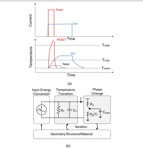
An SLC PRAM consists of two states, namely SET state corresponding to the low resistance crystalline phase or state“1”, and RESET state corresponding to the high re-sistance amorphous phase or state “0”. As shown in Figure 2a, in order to change the phase of a PRAM cell from one state to the other, there are two basic write operations: the SET operation that switches the GST into the crystalline phase and the RESET operation that switches the GST into the amorphous phase. For RESET operation, a large current is passed through top and bot-tom electrodes which heats the programmable region over its melting point. This is followed by a rapid quench which turns this region into an amorphous state. For SET, a lower current pulse is applied for a longer period of time
(a)
0 2 4 6 8 10 12 14
10k 100k 1M
Re
sista
n
ce(
)
Number of pulses
t
1t
2RC
t1: read and verify latency t2: programming pulse width(b)
so that the programmable region is at a temperature that is slightly higher than the crystallization transition temperature. For READ, a low voltage is applied between the top and bottom electrodes to sense the device resist-ance. The read voltage is set to be sufficiently high to pro-vide a current that can be sensed by a sense amplifier but low enough to avoid write disturbance [4].
To simulate the programming process of a PRAM cell, an HSPICE model has been developed as shown in Figure 2b. According to this model [18], the equivalent circuit of PRAM consists of four parts: input energy con-version, temperature transition, phase change, and geom-etry. HereRTandCTrepresent the thermal resistance and capacitance of GST structure,Rwriteis the electrical
resist-ance of GST during programming,RmandRg(T)represent
the phase of GST material, andCstaterepresents the state
of the MLC cell. The geometry block describes the cross-sectional shape (mushroom) of the PRAM cell, the dimen-sions of which are used to calculate the electrical and ther-mal parameters. The input energy changes the temperature of GST material based on RTand CT. The temperature evaluated by the temperature transition block is used to decide on the switch position; when the temperature is higher than the melting temperature, the switch flips up andCstateis charged by the voltage source,
indicating the melting of GST, which results in the amorphous phase. When the temperature is between the melting and annealing temperature, the switch flips down andCstateis discharged throughRg, indicating the
anneal-ing of GST, which results in the crystalline phase.
MLC PRAM
To increase the storage density of memory, MLC is used to store more than 1 bit within a single memory cell
[8,9]. Since the resistance between the amorphous and crystalline phases can exceed two to three orders of magnitude [3], multiple logical states corresponding to different resistance values can easily be accommodated. To study the programming process of MLC PRAM, the simulation model of SLC PRAM in Figure 2b can still be utilized. Note that while for SLC PRAM, the switch be-tween Rm and Rg(T) can only be set to “Rm” or “Rg(T)”
corresponding to amorphous or crystalline phase, for MLC PRAM, the switch is set to an intermediate pos-ition between the two ends.
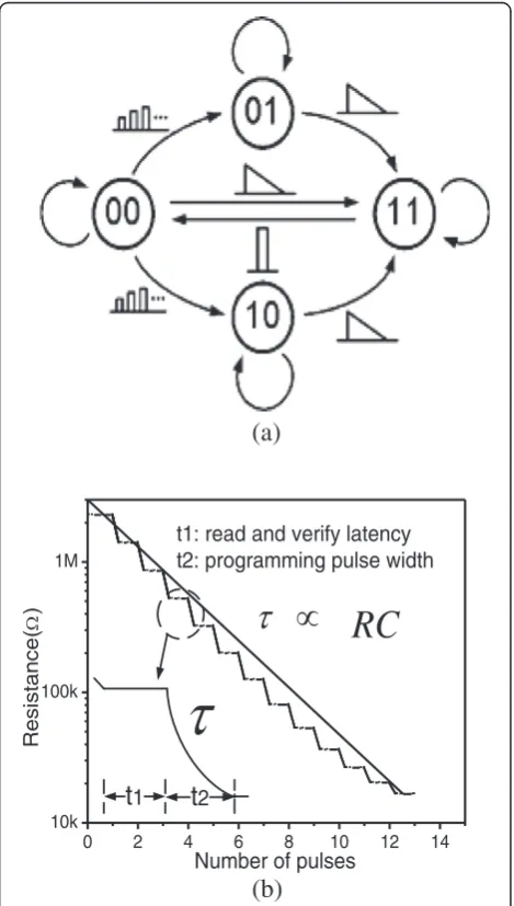
A 2-bit MLC PRAM consist of four states, where‘00’ is full amorphous state,‘11’ is full crystalline state,‘01’ and ‘10’are two intermediate states. The corresponding finite state machine (FSM) for modeling the WRITE strategy of a 2-bit MLC is shown in Figure 3a [19]. To go to ‘11’state, a ramp down SET pulse is applied. To go to‘00’state from a‘01’or‘10’state, it first transitions to‘11’state to avoid over programming, and then to‘00’ state. To write ‘01’or ‘10’, it first transitions to ‘00’state and then to the final state using several sequential short pulses. Figure 3b shows the resistance values corre-sponding to multiple programming steps that are required to go from‘00’state to‘10’state. The method is based on read and verify. During t1, the resistance value
in the memory cell is read out and compared with the resistance of the final state; if it is higher than the final state resistance, another current pulse of duration t2 is
applied to further lower the resistance. In this article, the static parameters used in the simulation of 2-bit MLC PRAM are listed in Table 1.
PRAM error model
Sources of soft and hard errors
The reliability of a PRAM cell can be analyzed with re-spect to data retention, cycling endurance, and data dis-turb [20]. Data retention represents the capability of storing data reliably over a time period and data reten-tion time is the longest time that the data can be stored reliably. We define ‘storage time’ as the time that the
00 01 10 11 Nu m b e r of ce lls N um be r of cel ls Rth(11,10) Failure cells Resistance 11 10 01 00 Resistance Rth(10,01) Rth(01,00) Rth(11,10) Rth(10,01) Rth(01,00)
(a)
(b)
Figure 4Resistance distribution of four states in 2-bit MLC PRAM.(a) Distribution in nominal mode. (b) An example of errors caused by the ‘01’resistance shift.
Table 1 Simulation parameters of a 2-bit MLC PRAM
2-bit MLC PRAM CMOS current driver
Parameter R00 R01 R10 R11 Vdd Width Length
data are stored in memory between two consecutive writes. Thus, the storage time has to be less than the data retention time. For PRAM, data retention depends on the stability of the resistance in the crystalline and amorphous phases. While the crystalline phase is fairly stable with time and temperature, the amorphous phase suffers from resistance drift and spontaneous crystallization. Initially, the resistance increases due to structure relaxation (SR) [10], a phenomenon seen in amorphous chalcogenides and related to the dynamics of the intrinsic traps. Eventu-ally, crystallization in the amorphous phase results in a drop in resistance and thereby loss of data in the cell. SR of the amorphous phase affects both resistance and threshold voltage of amorphous phase [21]. However, since the read region of the voltage is usually below the threshold voltage, only resistance drift is studied in this article. Resistance drift results in soft errors as will be described shortly.
Hard errors occur when the data value stored in one cell cannot be changed in the next programming cycle. There are two types of hard errors in PRAM: stuck-RESET failure and stuck-SET failure [20]. Stuck-SET or stuck-RESET means that the value of stored data in PRAM cell is stuck in SET or RESET state no matter what value has been written into the cell. These errors increase as the number of programming cycles increases. Data disturb, known as proximity disturb, can occur in a cell in RESET state if surrounding cells are repeatedly programmed. In this case, the heat generated during the programming operation diffuses from the neighboring cells and accelerates crystallization. Another type of dis-turb, read disdis-turb, occurs when a cell is read many times. This type of disturb is dependent upon the
applied cell voltage and ambient temperature. Both these types of disturb are not as prevalent and so in the rest of this section we focus on the effects of data retention and cycling endurance on the error rate.
The resistance distribution of a 2-bit MLC PRAM is shown in Figure 4a. The distributions of the intermediate states (‘01’and ‘10’) are shaped by the multiple-step pro-gramming strategy. There are three threshold resistances Rth(11,10),Rth(10,01), andRth(01,00)to identify the boundaries
between the four states. These resistances can be changed by tuning the reference current of the differential current amplifier during read sensing as has been demonstrated in MLC Flash memory architectures in [22]. Due to the change in the material characteristics such as SR or re-crystallization, the resistance distribution of logical states shifts from the initial position. Memory cells fail when the distribution crosses the threshold resistance level as shown in Figure 4b; the error rate is proportional to the extent of overlap. In this article, we assume that the initial resistance distribution is Gaussian. The mean values of the resistances have been listed in Table 1; the deviation is 0.17 as used in [11].
According to the proposed programming strategy, the resistances of intermediate states are always set back to the initial values in the next programming cycle. Thus, the effect of this resistance drift is cancelled in the next programming cycle and it only causes soft errors. A 10-5 10-4 10-3 10-2 10-1 100 101 102 103 104 105
104 105 106 107
Resistance(Ohm)
Time(s)
Symbols: measured data Lines: simulation data
00
01
10
11
e v A
t
R
t
t
R
=
+
=
R
(
)
0
%
40
/
σ
νμ
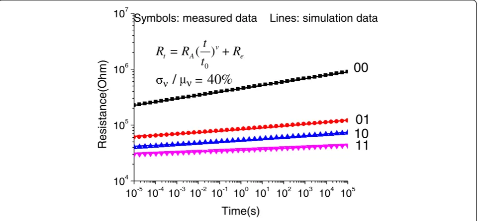
νFigure 5Resistance drift comparison between proposed MLC PRAM model and measured data [18].
Table 2 Parameters of resistance drift model
State 00 State 01 State 10 State 11
RA 225000 48319 15319 10026
simple model has been built to model resistance drift due to SR. Since RArepresent the amorphous active
re-gion exclusively, let Re represent the impact of all the
other resistances. Then, MLC PRAM time-dependent resistance is given by
Rt ¼RA
t t0
ν
þRe ð1Þ
where RAandReare varying andνis the resistance drift
coefficient, which is constant for all the intermediate states. Measured data from [23] almost match the
simulated data as shown in Figure 5. Note that in [11], is used to approximately fit measured data for short time periods. However, for longer time periods, this model is not accurate and gives a lower estimated soft error rate. In this article,νis set to 0.11, a typical value which has been used in [11,21], and the standard deviation to mean ratio is 40% as defined in [11]. Based on the initial resistance in Table 1,RAandRein this article are listed in Table 2.
Figure 6 describes the two mechanisms that result in soft errors. The error rate due to state ‘10’ crossing Rth(10,01) and state ‘01’ crossing Rth(01,00) depends on
the distributions of the resistances of states ‘10’ and
GST Resistance
1E0 1E5 1E10
1E-5
Time(s)
00
10 11
4s
ta
tes
of
PCRAM
cell
Resistance distribution Resistance drift
Soft Error Rate
00
01
10 11
Rth(01,00)
Rth(10,01) 01
Figure 6Soft error mechanism of MLC PRAM.
10
010
110
210
310
410
510
610
710
410
510
6Measured Resistance Simulated Resistance
Resistance(Ohm)
Number of programming cycles Resistance of state "00"
‘01’and the values of Rth(10,01) and Rth(01,00). Increasing
Rth(01,00) results in larger reduction in the soft error
rate, as will be shown later.
Stuck-SET failure is due to repeated cycling that leads to Sb enrichment at the bottom electrode [21]. Sb rich materials have a lower crystallization temperature leading to data loss and crystallization of the region above the bottom electrode at much lower temperatures than the original material composition. As a result, the bottom electrode cannot heat the GST material
sufficiently, and the resistance is lower than the desired level of reset state. The resistance drop can be analyzed as Ge density distribution change, similar to the trap density change for resistance drift. The re-sistance reduction is a power function of the number of programming cycles N and is given by ΔR=aNb. Figure 7 compares the resistance drop model of ‘00’ state with measured data from [24]. It shows that this model is fairly accurate; here a equals 151609 and b equals 0.16036.
GST Resistance
1E8 1E7
1E6
Number of write cycles
00
01
10
11
4
S
tate
s
of
P
CR
AM
cel
l
Resistance Distribution Resistance
drop Resistance of state “00”
Hard Error Rate
Rth(01,00)
Figure 8Hard error mechanism of MLC PRAM.
2 4 6 8
1E-7 1E-6 1E-5 1E-4 1E-3 0.01
Soft Error Rate
Log10 Time (s)
Es(10->01) Es(01->00):
Rth(01,00)=320K Rth(01,00)=360K Rth(01,00)=400K Rth(01,00)=440K
105s
In a stuck-RESET failure, the device resistance sud-denly and irretrievably spikes, entering a state that has much higher resistance than the normal RESET state. Stuck-RESET can also be caused by over programmed current [20]. Higher programming current results in lar-ger amorphous volume, which takes more time to be-come crystalline, shows higher resistance than desired value after a SET operation.
For SLC PRAM, most of the failures are stuck-SET failure. Since the resistances of intermediate states of MLC PRAM are guaranteed by read and verify steps in the write operation, the hard error mechanism of MLC PRAM is the same as that of SLC PRAM. Figure 8 shows how the resistance of ‘00’state drops over time. When the resistance distribution of state ‘00’ crosses Rth(10,01), hard errors occur.
5.0
5.2
5.4
5.6
5.8
6.0
10
-810
-710
-610
-510
-410
-310
-2Hard error rate
Log
10(Pcycles)
R
th(01,00):
320k
360k
400k
440k
480k
Figure 10Hard error rate as a function ofRth(01,00)and number of programming cycles (Pcycles).
10 15 20 25 30 35 40 45 50 1E-8
1E-7 1E-6 1E-5 1E-4 1E-3 0.01 0.1
Rth(01,00) (10K Ohm)
Error rate
Soft error Hard error Total error
Constant region Decreasing region
Circuit-level techniques for reducing soft and hard errors
In the previous section, we have shown that the soft error rate increases with data storage time and that the hard error rate increases with the number of program-ming cycles. In this section, we show how the error rate can be controlled by tuning the threshold resistance Rth (00,01)for a specific data storage time. Recall that
thresh-old resistance can be tuned by changing the current reference of the sense amplifier. Data storage time is set
to 105 s, which is typical of storage systems such as those for daily backup.
However, if data storage time distribution is known a priori, then a better estimate of this time can be used to derive the threshold resistance.
Soft error rate
The soft error rate of 2-bit MLC PRAM is a function of the resistance drift of‘01’to‘00’state,Es(‘01’- >‘00’), and
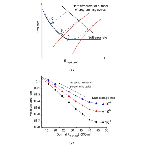
Soft error rate Hard error rate for number
of programming cycles
A B C
) 00 , 01 (
th
R
Error
rate
(a)
(b)
15 20 25 30 35 40 45 50
1E-8 1E-7 1E-6 1E-5 1E-4 1E-3 0.01 0.1
10
610
5Minimum error rate
Optimal Rth(01,00)(10KOhm)
Data storage time
10
4I
ncreased number of programming cyclesthe resistance drift of ‘10’ to ‘01’ state, Es (‘10’- >‘01’).
While Es (‘01’- >‘00’) depends on the value of Rth(01,00),
Es(‘10’- >‘01’) depends on the value ofRth(10,01).
Figure 9 describes how the soft error rate increases with data storage time for different values of Rth(01,00).
Here, Rth(01,10) is set as the middle value between
resis-tances of ‘01’and‘10’states, which is 30.5K in this case. Tuning this resistance is difficult because of the close spacing between the distributions of the ‘01’ and ‘10’ states. In this scenario, however, Rth(01,00) has a much
higher impact on the total soft error rates; as Rth(01,00)
increases, the soft error rate reduces.
In order to counteract the effect of resistance drift, dy-namicRth(01,00)and Rth(10,01)tuning has been proposed in
[11]. Here, a time tag is used to record the storage time in-formation for each memory block or page and this infor-mation is used to determine the threshold resistance that minimizes the BER. The technique in [11] considers the effect of resistance drift on soft errors. The threshold re-sistance value affects the hard error rate as well and so the
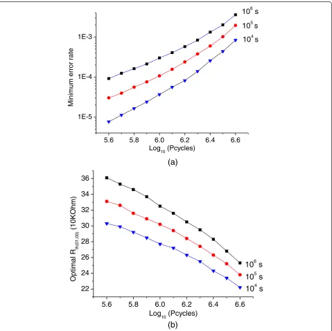
(a)
(b)
5.6 5.8 6.0 6.2 6.4 6.6
1E-5 1E-4 1E-3
10
5s
10
6s
Minimum error rate
Log10 (Pcycles)
10
4s
5.6 5.8 6.0 6.2 6.4 6.6 22
24 26 28 30 32 34 36
10
4s
10
5s
Optimal R
th
(0
1,
00)
(10KOhm)
Log10 (Pcycles)
10
6s
choice of threshold resistance has to be determined by both soft and hard error rates as will be described next.
Hard error rate
The hard error rate of 2-bit MLC PRAM is due to the resistance drop of ‘00’state to the ‘01’state as shown in Figure 7. It is a function of Rth(01,00), and the resistance
distribution of state 00. Due to multiple pulse write strategy for intermediate states, there is no resistance drop from ‘01’ state to ‘10’state, and thus Rth(10,01) has
no impact on the hard error rate.
Figure 10 shows the hard error rate as a function of the number of programming cycles for different values ofRth(01,00). We see that for a specificRth(01,00), the hard
error rate increases exponentially with number of pro-gramming cycles. It also shows that for a specific number of programming cycles, lower threshold resist-ance results in lower hard error rate. Therefore, lower Rth(01,00)results in fewer hard errors.
Total error rate
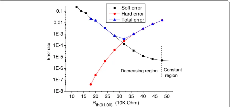
Consider a scenario where the number of programming cycles is 106 and the data storage time is 105 s. Since
both the hard error and soft error rates are a function of Rth(01,00), we combine the two error rates in Figure 11
and present them as a function ofRth(01,00). We see that
while the hard error rate increases monotonically, the soft error rate curve decreases at first and then becomes constant. Soft error rate keeps decreasing till a critical Rth(01,00) is reached, which is 440K in this case. It then
maintains a constant value which is determined by the error rateEs (‘10’-> ‘01’). From the plot we see that the
lowest total error occurs atRth(01,00)of 320K.
Figure 12 generalizes the above procedure. Figure 12a shows how for a specific data storage time (given by soft error curve), the optimalRth(01,00)reduces as the number
of programming cycles increases. Figure 12b provides the lowest error rate values as a function of optimal Rth(01,00)for three data storage times. As the data storage
time increases, the error rate increases, as expected. Figure 13a shows that for a fixed data storage time, as the number of cycles increases, the total BER increases. Figure 13b shows the corresponding values of Rth(01,00).
The advantage of threshold resistance tuning is that it provides an easy way of achieving the lowest possible error rate considering both soft and hard errors. From Figure 11,
Serial Sense Reference
Decoder Sense Amplifier
BL Selection
Odd BL Even BL
Rth(01,00) Rth(10,01)Rth(11,10)
WL FG
Rth(01,00)Tuning
Control
we can see that for a specific case of 2-bit MLC PRAM, in which the effective data storage time is 105s at 106 pro-gramming cycles, the total BER has been reduced from 10–2 to about 10–4. Reducing the error rate any further with circuit-level tuning is costly. In“ECC schemes” sec-tion, we show how ECC techniques can be used in con-junction with threshold resistance tuning to achieve significantly lower BER with much lower overall cost.
Tuning threshold resistance
Figure 14 shows how the serial sense amplifier used in the MLC Flash architecture [25] can be used to support vary-ing threshold resistance for 2-bit MLC PRAM. The float-ing gates (FG) in the access transistors (controlled by WL) are used to set the values of Rth(01,00), Rth(10,01), and Rth (11,10). The different resistances result in different reference
currents in this circuit. The three reference resistances are selected by the sense reference decoder in a serial order to determine whether the bits that were read out are‘00’,‘01’, ‘10’, or‘11’. Further tuning ofRth(01,00)can be achieved by
introducing a second level of selection transistors to select the specific FG transistor. The Rth(01,00) tuning block
makes the selection based on the optimalRth(01,00) value.
Recall that this value changes with data storage time and number of programming cycles and so dynamic tuning is desirable. Figure 14 shows a three-FG design forRth(01,00);
for finer tuning, more FGs are required.
STT-RAM reliability
In this section, we describe the basic structure of the STT-RAM cell including its read/write operations (see the next section), sources of its errors (see“STT-RAM error model” section), and circuit-level techniques to reduce them (see “Circuit-level techniques for reducing error”section).
Background
In STT-RAM, the resistance of the MTJ determines the logical value of the data that are stored. MTJ consists of a thin layer of insulator (spacer-MgO) about approximately 1-nm thick sandwiched between two layers of ferromag-netic material [5]. Magferromag-netic orientation of one layer is kept fixed and an external field is applied to change the
orientation of the other layer. Direction of magnetization angle (P or AP) determines the resistance of MTJ which is translated into storage; P corresponds to storage of bit 0 and AP corresponds to storage of bit 1. Low resistance (P) state is accomplished when magnetic orientation of both layers is in the same direction. By applying external field higher than critical field, magnetization angle of free layer is flipped by 180° which leads to a high resistance state (AP). The difference between the resistance values of P and AP states is called tunneling magneto-resistance (TMR) which is defined asTMR¼RAP¼RP
RP whereRAPand RPare the resistance values at AP and P states. Increasing
the TMR ratio makes the separation between states wider and improves the reliability of the cell [7]. Figure 15 describes the cell structure of an STT-RAM and high-lights the P and AP states.
A physical model of MTJ based on the energy inter-action is presented. Magnetization angle of the free layer is determined based on the dimensions of MTJ and the external field applied. Energies acting in MTJ are Zeeman, anisotropic, and damping energy [25]. These energy types determine the change in magnetic orientation, alignment of the magnetization angle along the fixed axis and are used to form the Landau– Lifshitz–Gilbert equation. The stable state of MTJ corre-sponds to minimum total energy. State change of MTJ cell can be derived by combining these energy types:
dM!
dt ¼ μ0⋅Ms⋅H
!
þ α
Ms⋅
M! dM
!
dt
þKsinθcosθ ð2Þ
θ
(a)
(b)
(c)
Free Layer
Pinned Layer Dielectric
(MgO)
I I
θ
Figure 15STT-MRAM structure: (a) P, (b) AP, (c) MTJ circuit structure.
Table 3 Device parameters of STT-RAM
Nominal Variance
Transistor channel length(nm) 32 5%
Transistor channel width (nm) 96, 128, 160 5%
Transistor threshold (RDF) 0.4 V σVT=40 mV
Rp(P) 2.25K Approximately 6%
RAP(AP) 4.5K Approximately 6%
where M! is magnetic moment, μ0is vacuum
permeabil-ity, α is damping constant. Such an equation can be modeled using Verilog-A to simulate the circuit charac-teristics of STT-RAM. For instance, differential terms are modeled using capacitance while Zeeman and damping energy are described by voltage-dependent current source. The voltage of the capacitor indicates the evalu-ated state (magnetization angle) which is further trans-lated to resistance of MTJ.
Consider the cell structure consisting of an access tran-sistor in series with the MTJ resistance illustrated in Figure 15c. The access transistor is controlled through WL, and the voltage levels used in BL and SL lines deter-mine the current which is used to adjust the magnetic field. There are three modes of operation for an STT-RAM: write-0, write-1, and read. We distinguish between
write-0 and write-1 because of the asymmetry in their op-eration. In general, directions of the current during write-0 and read operation are the same, while the magnitude of the current is fairly high (approximately 10×) during the write operation. For read operation, current (magnetic field) lower than critical current (magnetic field) is applied to MTJ to determine its resistance state. Low voltage (ap-proximately 0.1 V) is applied to BL, and SL is set to ground. When the access transistor is turned on, a small current passes through MTJ whose value is detected based on a conventional voltage sensing or self-referencing schemes [26]. During write operation, BL and SL are charged to opposite values depending on bit value that is to be stored. During write-0, BL is high and SL is set to zero, whereas during write-1, BL is set to zero and SL is set to high. The asymmetric structure of write-0 and Figure 16Failures occur when the distributions of read-0 and read-1 current overlap.
write-1 operations motivates SL line to be higher than nominal during write-1 so that both operations generate comparable write-current. Such a circuit technique is ela-borated in the next section.
STT-RAM error model
There are several factors that affect the failure in STT-RAM memories: access transistor manufacturing errors such as those due to RDFs, channel length, and width modulations, geometric variations in MTJ such as area and thickness variation, and thermal fluctuations that are modeled by the initial magnetization angle variation [15]. Note that all these variations cause hard errors.
Apart from errors that are caused by process varia-tions, MTJ also suffers from time-dependent reliability
issues. MTJ structure consists of a very thin insulating layer (approximately 1 nm) and voltage across MTJ can approximately be 0.6–1 V. This results in a very high electric field across the thin insulator (approximately 10 MV/cm) which can cause time-dependent dielectric breakdown (TDDB). With high scaling, the electric field across insulating layer rises, thereby increasing the possi-bility of TDDB.
Next we consider the effect of key process variation factors on the error rate. The effect of RDF on threshold voltage is typically modeled with an additive independ-ent and idindepend-entically distributed (i.i.d.) Gaussian distribu-tion. Variance of threshold voltage of a MOSFET is proportional to σVT:LEOTtWt, where EOT is oxide thick-ness, and Lt and Wt are length and width of the
Table 4 BERs of a single STT-RAM cell
Read (Vread= 0.1 V) Write (pulse width = 25 ns)
0 1 0 1
Approximately 10–5 Approximately 10–5 Approximately 4 × 10⁻⁵
(a)
(b)
39%
8%
44%
9%
Transistor V
thTransistor
W/L
MTJ Geometry
MTJ IA
MTJ AI
20%
1%
37%
42%
Transistor V
thTransistor
W/L
MTJ Geometry
transistor, respectively. For 32 nm, σVTis approximately between 40 and 60 mV [27]. We model CMOS channel length and width variation using i.i.d. Gaussian distribu-tion with 5% variadistribu-tion. These variadistribu-tions induce change in the drive current of the transistor which results in in-crease on variation in both read and write operations. Variation in tunneling oxide thickness tOX(MTJ)and
sur-face area AMTJ of MTJ are the main causes behind the
random resistance change in MTJ material. Resistance of the MTJ is proportional to / 1=AMTJ
etoxðMTJÞ [13]. In
our simulations, we set the nominal values of (Rp) to
2.25K and (RAP) to 4.5K and modeled the variations
using i.i.d. Gaussian distribution with 2% variance for thickness and 5% variance for the area [13]. Further-more, initial magnetization angle of the MTJ affects the duration of the write operation, since it induces extra
resistance when the angle is not aligned properly at the initial state. Such variation is also modeled using i.i.d. Gaussian distribution with 0.1 radian variance [7]. The nominal values and variance of the device parameters are listed in Table 3. We consider 40 mV variation for RDF when width of 128 nm which is equivalent to W/L= 4 and scaled it for differentW/Lratios.
Errors in read and write operations
The reliability of an STT-RAM cell has been investigated by several researchers. While Chatterjee et al. [7] studied the failure rate of a single STT-RAM cell using basic models for transistor and MTJ resistance, process vari-ation effects such as RDF and geometric varivari-ation were considered in [15,28]. In this section, we also present the effects of process variation and geometric variation. We add the variation effects to the nominal HSPICE model Figure 19Distribution of read current for different access transistor sizes.
of STT-RAM and use Monte Carlo simulations to gener-ate the error rgener-ates caused by each variation.
Read operation During read operation, BL is set to 0.1 V, SL is set to ground and the stored value is determined based on the current passing though the MTJ. Figure 16 describes the read current distributions for 32 nm tech-nology (nominal voltage is 0.9 V) for transistorW/L= 4. Threshold current value is used to distinguish between two states (read-0 and read-1). Typically, there are two main types of failures that occur during the read oper-ation: read disturb and false read. Read disturb is the re-sult of the value stored in the MTJ being flipped because of large current during read. False read occurs when the current of P (AP states) crosses the threshold value of the AP (P) state as illustrated in Figure 16. In our
analysis, we find that the false read errors are dominant during the read operation, thus we focus on false reads in the error analysis.
Write operation During write 0, BL is high and SL is set to zero whereas during write-1 BL is set to zero and SL is set to high. Figure 17 illustrates the write-0 time distribution of an STT-RAM cell for access transistor size of W/L = 4, BL = 0.9 V, SL = 0. We observe that such a distribution has a long tail unlike a Gaussian dis-tribution. During write operation, failures occur when the distribution of write latency crosses the predefined access time as illustrated in Figure 17. Write-1 is more challenging for an STT-RAM device due to the asym-metry of the write operation. During write-1, access transistor and MTJ pair behaves similar to a source Figure 21Probability distribution of write-0 and write-1 for different values of SL voltage.
follower which increases the voltage level at the source of the access transistor and reduces the driving write current. Such a behavior increases the time required for a safe write-1 operation.
Table 4 shows the BER for read and write operations of STT-RAM at nominal conditions corresponding to Vdd= 0.9V, write pulse = 25ns, Vread= 0.1V and access
transistor size of W/L = 4. Write-1 has very high BER compared to write-0 which has a BER of 10–5. The effect of such asymmetry in write operation on system reliabil-ity has also been presented in [13,28].
The variation impacts of the different parameters are presented in Figure 18 for read and write operations. To generate these results, we changed each parameter one at a time and did Monte Carlo simulations to calculate the contribution of each variation on the overall error rate. We see that variation in access transistor size is very effective in shaping the overall reliability; it affects the read operation by 37% and write operation by 44% with the write-0 and write-1 having very similar values. The threshold voltage variation affects the write oper-ation more then the read operoper-ation. Finally, the MTJ Figure 23Power and energy consumption for different values of boosted voltage and write pulse width.
2 3 4 5 6 7 8 9 10
10-10 10-9 10-8 10-7 10-6 10-5 10-4 10-3
10-4
Block failure rate
Error correction capability (t)
512 at raw BER 10-4 1k at raw BER 10-4 2k at raw BER 10-4 512 at raw BER 10-5 1k at raw BER 10-5 2k at raw BER 10-5
10-5
512bit 10-3
geometry variation is more important in determining the read error rate as illustrated in Figure 18b.
Circuit-level techniques for reducing error
In this section, we show how W/Lsizing of access tran-sistor, voltage boosting, and pulse width adjustment can be used to improve the reliability of the STT-RAM cell. Access transistor sizing has been investigated in [7,13], effect of process variation as well as write pulse width has been studied in [13,14,28] and voltage boosting of WL has been considered in [13,29]. Here, we also study the read reliability and investigate the effect of combin-ation of write pulse width and voltage boosting on the write reliability.
Effect of W/L of access transistor
The width of the access transistor has two effects on the read current distribution: it reduces the effect of RDF variation and improves the reliability by increasing the distance between the mean of the read-0 and read-1 dis-tributions. Figure 19 illustrates this phenomenon by plotting the read current distributions for three W/L ratios of the access transistor. Thus based on the W/L ratios we can choose the threshold value that maximizes the detection probability, which in return minimizes the BER. For instance, when W/L= 3, BER = 0.7 × 10⁻⁴; it reduces to BER = 2.5 × 10⁻⁵when the size increases to W/L=5. Even though increasing W/Limproves the reli-ability for the read operation, it reduces the cell density and increases the power consumption.
We also looked at the effect of W/Lratio on write fail-ure. WhenW/Lratio of the access transistor increases, its current driving capability is enhanced and the necessary time duration for a successful write operation is reduced. Figure 20 illustrates the BER versus write time duration of a write-1 operation for three different values ofW/L.
Effect of voltage boosting
Gate level (WL) voltage boosting has been investigated in [13,29] to reduce the write-1 latency of STT-RAM. It is an effective way of increasing the drive current of access tran-sistor which leads to reduction in latency. However, WL boosting requires separate WLs for write-0 and write-1 operations. Two-step writing, erase/program schemes have been proposed to overcome the limitations; however, all the schemes incur extra latency or energy consump-tion. We propose boosting SL during write operation to improve the write-1 reliability. This method enables re-duction of the pulse duration for write-1 operation while incurring very small overhead. Figure 21 illustrates the la-tency distribution of write-1 operation when access tran-sistor size isW/L= 4, BL is set to zero and SL varied from 0.9 (nominal) to 1.5 V. We see that boosting SL voltage level over nominal voltage level reduces the average la-tency and variation of the write-1 operation. The distribu-tions of write-0 at nominal voltage and write-1 when the supply voltage is boosted up to 1.5 V have almost identical characteristics. If the pulse width for both write-0 and write-1 operations are the same, the energy consumptions are comparable. This is because the write current of write-1 operation at write-1.5 V SL voltage is comparable to that of write-0 operation at nominal voltage (BL = 0.9 V).
Effect of combination of voltage boosting and write pulse width duration
Figure 22 illustrates the BER of write-1 operation under different voltage levels and write pulse width for access transistor size of W/L = 4. As expected, increasing the Table 5 ECC scheme for STT-RAM and PRAM to achieve the target BFR
512 bits 1024 bits 2048 bits
STT-RAM BCH(542,512) BCH(1057,1024) BCH(2084,2048)
PRAM BCH(552,512) BCH(1079,1024) BCH(2120,2048)
128 information bits BCH(144,128)
128 information bits
128 information bits
...
16
sub-block
16 parity bits
16 parity bits 16 parity bits
128 Even parity check 16 parity bits
Even parity check(17,16) 1
2
16
17
pulse width reduces the BER for both write-0 and write-1 operations. Furthermore, boosting voltage level of SL dur-ing write-1 operation also reduces the write-failures. For
instance, when pulse width is 30 ns, write-1 BER = 0.25 × 10⁻²when the boosted voltage is 1.1 V, whereas write-1 BER = 0.4 × 10⁻⁴when the boosted voltage is 1.3 V.
(a)
(b)
10-5 10-4 10-3 10-12
10-11 10-10 10-9 10-8 10-7 10-6 10-5 10-4 10-3 10-2 10-1
106.2
Block failure rate
Raw BER
BCH(1079,1024) BCH(78,64)*16
BCH(78,64)*16+even parity check BCH(144,128)*8
BCH(144,128)*8+even parity check
Pcycles 105.5
10-5 10-4 10-3 10-12
10-11 10-10 10-9 10-8 10-7 10-6 10-5 10-4 10-3 10-2 10-1 100
106.0
Block failure rate
Raw BER
BCH(2120,2048) BCH(144,128)*16
BCH(144,128)*16+even parity check BCH(274,256)*8
BCH(274,256)*8+even parity check
105.3 Pcycles
Figure 26Performance comparison between long BCH code and flexible ECC scheme for (a) 1024 bits and (b) 2048 bits.
Table 6 Extra storage rates of different ECC schemes for three block sizes
BCH(78,64)*8+ even parity check
BCH(78,64)*16+ even parity check
BCH(144,128)*8+ even parity check
BCH(144,128)*16+ even parity check
BCH(274,256)*8+ even parity check
512 bits 27%
1024 bits 22.8% 21%
In general, increasing these parameters reduces BER, but causes higher energy consumption per operation. For instance, let the average BER (read/write combined) after circuit-level techniques be set to 10–5. From read failure analysis, we see that W/L = 4 achieves approxi-mately BER = 10–5. Even though, increasing W/L ratio improves the reliability for both read and write opera-tions, it reduces the cell density and increases the energy consumption. Thus, it should be applied with caution and other options investigated.
Next, we investigate the combination of different write pulse widths and boosted SL voltages that can achieve the same target BER. For BER = 10–5, we consider the following combinations of write pulse widths and boosted voltages: (60 ns, 0.9 V), (42 ns, 1.1 V), (31 ns, 1.3 V), and (25 ns, 1.5 V). Figure 23 illustrates the nor-malized average write power and energy consumption for all four cases. Since the average energy consumption of each write operation is comparable, higher voltage levels for write operation becomes more attractive due to its lower latency. However, increasing voltage also may create problems of MOSFET degradation due to hot carrier injection. Based on this analysis, we choose write pulse width of 31 ns and SL voltage of 1.3 V that achieves BER of approximately 10–5. While this is a sig-nificant reduction in the BER, for reliable memory operations, the target error rate is a lot lower. Such error rates are not achievable using only circuit-level techni-ques or using only ECC. In the following section, we de-scribe our approach of applying ECC on top of circuit-level techniques to achieve high circuit-level of reliability with reduced cost.
ECC schemes
ECC performance
One of the effective techniques to reduce the error rate in memories is through ECC. As described in “PRAM reliability”and“STT-RAM reliability”sections, raw error rate of MLC PRAM and STT-RAM can significantly be reduced using circuit-level techniques. For instance, the error rate of MLC PRAM can be reduced to 10–4 by adjusting Rth(10,00) and the error rate of STT-RAM can
be reduced to 10–5 by voltage boosting and/or write pulse width adjustment.
In this section, we consider BFR as the performance metric since it represents the decoding performance more accurately compared to BER. The BFR for a con-stant block size Nis calculated using a binomial distri-bution of uniform errors as:
BFR¼Pðerror>tÞ ¼ X
N
i¼tþ1 N
i BER
ið1BERÞNi ð
3Þ
where tis the correction strength of the ECC, and BER represents the raw error rate after applying circuit-level techniques.
In this article, the target BFR is set to 10–8. For STT-RAM, this target is constant during the whole lifetime. For PRAM, the error rate increases with number of pro-gramming cycles. Our goal is to maintain the same BFR throughout the devices’lifetime.
To achieve the target BFR for both STT-RAM and PRAM, performances of ECC schemes with different error correction capabilities are shown in Figure 24. Three Table 7 Synthesis results of all candidate BCH codes
Encoder Syndrome KES Chien search
Area (μm2) Power (μw) Area (μm2) Power (μw) Area (μm2) Power (μw) Area (μm2) Power (μw)
BCH(144,128) 118 16 341 67 1404 248 188 300
BCH(542,512) 177 21 583 118 1836 478 244 444
BCH(1057,1024) 192 23 629 123 2145 533 286 489
BCH(2084,2048) 217 28 680 140 2618. 669 328 578
BCH(552,512) 236 28 780 171 1978 512 392 699
BCH(1079,1024) 353 46 1133 233 3700 945 545 963
BCH(2120,2048) 430 56 1378 1354 4236 424 664 1203
Critical path is 0.59 ns for BCH(144,128), 0.65 ns for BCH(542,512), BCH(552,512), 0.74 ns for BCH(1057,1024), BCH(1079,1024), 0.89 ns for BCH(2084,2048), BCH (2120,2048).
Table 8 Hardware overhead of ECC scheme for STT-RAM
Energy (pJ) Latency (ns) Area Extra storage rate (%)
512 bits BCH(542,512) 42.4 85.6 2840 5.5
1024 bits BCH(1057,1024) 100.4 192.5 3525 3.1
block sizes namely 512, 1024, and 2048 bits are studied. The bottom three curves correspond to STT-RAM which can achieve raw BER of 10–5 by circuit-level techniques. We see that t = 3 codes are sufficient to achieve BFR ≤ 10–8for all three block sizes. The top curves correspond to MLC-PRAM which achieves 10–4by circuit-level tech-niques. We see that to meet BFR ≤10–8, stronger codes have to be adopted for large block size. For instance for block size 2K,tequals to 6. The advantage of circuit-level techniques is also demonstrated in Figure 24. For a 512-bit block size, when the raw BER can be reduced from 10–3to 10–4, it is sufficient to consider ECC witht= 4 (instead oft= 8). Using a weaker code results in signifi-cant reduction in the ECC overhead. The ECC schemes in Figure 24 are listed in Table 5.
The raw error rate of MLC PRAM increases as the number of programming errors increases. Thus, a flex-ible ECC scheme that can support higher error correc-tion capability over time is desirable. Flexible ECC scheme is implemented by using product code which corrects errors in two dimensions. When the number of programming cycles is low, it is sufficient to do ECC in one dimension. As the number of programming cycles increases, the flexible ECC scheme uses ECC in two dimensions to enhance the error correction capability.
The structure of product code for a 2048-bit block is shown in Figure 25. The data are organized into 16 sub-blocks with BCH(144,128) operating on each subblock. During encoding, even parity check encoding is done along columns and BCH encoding is done along rows. The even parity encoder generates a 17th subblock on which BCH encoding is also done. During decoding, 17 BCH codes are decoded in the order from the 17th to the 1st followed by parity check. BCH(144,128) can correct two errors and detect more than two errors. After BCH decoding, the subblocks that contain more than two errors are marked and the position of the remaining errors in the marked subblock is detected by even parity check.
Performance comparison for 1K and 2K bit block sizes are shown in Figure 26. For 1K bit block size, both BCH (78,64) × 16 with even parity and BCH(144,128) × 8 with even parity meet the target BFR for raw BER of 10–4. BCH(78,64) × 16 with even parity is preferred because it has lower BFR as shown in Figure 26a. For 2K bit block size, before 105.3 = 2 × 05 programming cycles, regular BCH(144,128) × 16 is sufficient to ensure
that the BFR is lower than 10–8. After 2 × 10⁵ program-ming cycles, when the raw BER increases to 10–4 even parity check is done in conjunction with BCH(144,128) to guarantee the same target BFR of 10–8.
Next, we present redundancy rate of the different ECC schemes. As shown in Table 6, the redundancy rate of product codes for 512-bit block and 1024-bit block is more than 20%. Thus, to keep the redundancy rate of memory below 20%, we only propose the flexible ECC scheme for 2048-bit block. Between two candidate flex-ible schemes for 2048 bits block, BCH(144,128) × 16 with even parity check is preferred because it has lower redundancy rate as shown in Table 6 and lower BFR as shown in Figure 26.
Hardware overhead
The BCH codes used for STT-RAM and PRAM have been synthesized in 45 nm technology using Nangate cell library [30] and Synopsys Design Compiler [31]. The synthesis results are listed in Table 7. BCH decoders use pipelined simplified inverse-free Berlekamp-Massey (SiBM) algorithm. The 2t-fold SiBM architecture [32] is used to minimize the circuit overhead of Key-equation solver while its latency is maximized. A P factor of 8 is used for all the syndrome calculation and Chien search circuitries. All the power numbers are simulated when the clock period is set to the critical path, which equals to the delay of 1 Galois field multiplier and 1 Galois field adder.
The energy, latency, area, and redundancy rate of the ECC schemes for STT-RAM are shown in Table 8. Since the error rate of STT-RAM does not change with data storage time or number of programming cycles, it only uses the ECC scheme BCH(2084,2048) on block size of 2048 bits to achieve BFR = 10–8.
The comparison of energy, latency, area, and redun-dancy rate of the ECC schemes for MLC-PRAM are shown in Table 9. For 2K bits, to achieve BFR of 10–8, we could use BCH(2120,2048) or the flexible scheme which migrates from BCH(144,128) to BCH(144,128) with even parity when the raw BER increases from 1.5 × 10⁻⁵to 10–4due to increased number of programming cycles. Although the redundancy rate of flexible scheme is significantly higher than BCH(2120,2048), it is still <20% and its ECC energy consumption is only 17% of BCH(2120,2048). Moreover, the latency of the flexible Table 9 Hardware overhead of ECC scheme for MLC-PRAM
Energy (pJ) Latency (ns) Area Extra storage rate (%)
512 bits BCH(552,512) 56.3 86.5 3386 7
1024 bits BCH(1079,1024) 187.8 194.5 5732 5.9
2048 bits BCH(2120,2048) 585.5 463.7 6717 1.7
ECC scheme is 38% of BCH(2120,2048) because it has shorter critical path and the BCH(144,128) units can be pipelined as in [32].
Conclusion
In this article, we advocate the use of circuit parameter tuning and ECC to improve the reliability of emerging memory technologies such as MLC-PRAM and STT-RAM. We first analyze the error sources and build error models for these two technologies. Next we show that for MLC-PRAM, the hard and soft error rates can be reduced by optimal choice of threshold resistance. Simi-larly for STT-RAM, the hard error rate can be reduced by tuning theW/Lratios of the access transistors, boost-ing the voltage, and adjustboost-ing the write pulse width. These circuit-level techniques can help achieve BER of 10–4to 10–5. For higher reliability, ECC techniques have to be used in conjunction with the circuit techniques. We show that for STT-RAM, it is sufficient to use a BCH code with t = 3 to achieve a BFR of 10–8. For MLC-PRAM, the raw BER increases with time and num-ber of programming cycles and so a flexible ECC scheme that migrates to a stronger code is desirable. We propose one such product code scheme that uses BCH along rows and even parity along columns and achieves the desired BFR. We synthesize the ECC schemes in hard-ware and show that the hardhard-ware overhead, including additional storage, is quite low, making these schemes very attractive.
Competing interests
The authors declare that they have no competing interests.
Acknowledgment
This study was supported in part by a grant from NSF, CSR 0910699, and CNS 1218183. The authors would like to acknowledge the assistance from Zihan Xu and Ketul Sutaria on the memory modeling work.
Received: 16 April 2012 Accepted: 20 August 2012 Published: 3 October 2012
References
1. BC Lee, E Ipek, O Mutlu, D Burger, Architecting phase change memory as a scalable DRAM alternative, inInternational Symposium on Computer Architecture(2009), pp. 1–12
2. X Wu, J Li, L Zhang, E Speight, R Rajamony, Y Xie, Hybrid cache architecture with disparate memory technologies, inInternational Symposium on Computer Architecture(Austin, Texas, USA, 2009), pp. 34–45
3. GW Burr, MJ Breitwisch, M Franceschini, D Garetto, K Gopalakrishnan, B Jackson, B Kurdi, C Lam, LA Lastras, A Padilla, B Rajendran, S Raoux, RS Shenoy, Phase change memory technology. J Vac Sci Technol B
28(2), 223–262 (2010)
4. HS Philip Wong, S Raoux, S Kim, J Liang, JP Reifenberg, B Rajendran, M Asheghi, KE Goodson, Phase change memory. Proc IEEE98, 2201–2227 (2010)
5. T Kawahara, R Takemura, K Miura, J Hayakawa, S Ikeda, Y Lee, R Sasaki, Y Goto, K. Ito, I Meguro, F Matsukura, H Takahashi, H Matsuoka, H Ohno, 2 Mb SPRAM (spin-transfer torque RAM) with bit-by-bit bi-directional current write and parallelizing-direction current read. IEEE J Solid State Circuits
43(1), 109–120 (2008)
6. W Xu, H Sun, X Wang, Y Chen, T Zhang, Design of last level on-chip cache using spin transfer torque RAM. IEEE Trans VLSI Syst
19(3), 483–493 (2011)
7. S Chatterjee, M Rasquinha, S Yalamanchili, S Mukhopadhyay, A scalable design methodology for energy minimization of STTRAM: a circuit and architecture perspective. IEEE Trans VLSI Syst19(5), 809–817 (2011) 8. XQ Wei, LP Shi, R Walia, TC Chong, R Zhao, XS Miao, BS Quek, HSPICE macro model of PCRAM for binary and multilevel storage. IEEE Trans Electron Dev53(1), 56–62 (2006)
9. N Papandreou, A Pantazi, A Sebastian, M Breitwisch, C Lam, H Pozidis, E Eleftheriou, Multilevel phase-change memory, in17th IEEE International Conference on Electronics, Circuits, and Systems (ICECS)(, Athens, Greece, 2010), pp. 1017–1020
10. S Lavizzari, D Ielmini, D Sharma, AL Lacaita, Reliability impact of chalcogenide-structure relaxation in phase-change memory (PCM) cells— Part II: physics-based modeling. IEEE Trans Electron Dev56, 1078–1085 (2009)
11. W Xu, T Zhang, A time-aware fault tolerance scheme to improve reliability of multi-level phase-change memory in the presence of significant resistance drift. IEEE Trans VLSI Syst19(8), 1357–1367 (2011) 12. H Sun, C Liu, N Zheng, T Min, T Zhang, Design techniques to improve
the device write margin for MRAM-based cache memory, inACM Great Lakes Symposium on VLSI(, Lausanne, Switzerland, 2011), pp. 97– 102
13. Y Zhang, X Wang, Y Chen, STT-RAM cell design optimization for persistent and non-persistent error rate reduction: a statistical design view, inIEEE/ ACM International Conference on Computer Aided Design(San Jose, CA, USA, 2011), pp. 471–477
14. J Lo, C Augustine, S Salahuddin, K Roy, Modeling of failure probability and statistical design of spin-transfer magnetic random access memory (STT MRAM) array for yield enhancement, inIEEE Design Automation Conference
(Anaheim, CA,USA, 2008), pp. 278–283
15. A Nigam, CW Smullen, V Mohan, E Chen, S Gurumurthi, MR Stan, Delivering on the promise of universal memory for spin transfer torque RAM (STT-RAM), inInternational Conference on Low Power Electronics and Design
(Fukuoka, Japan, 2011), pp. 121–126
16. C Yang, Y Emre, Y Cao, C Chakrabarti, Multi-tiered approach to improving the reliability of multi-level cell PRAM, inIEEE Workshop on Signal Processing Systems(Quebec, Canada, 2012)
17. Y Emre, C Yang, K Sutaria, Y Cao, C Chakrabarti, Enhancing the reliability of STT-RAM through circuit and system level techniques, inIEEE Workshop on Signal Processing Systems(Quebec, Canada, 2012)
18. Z Xu, K Sutaria, C Yang, C Chakrabarti, Y Cao, Hierarchical modeling of phase change memory for reliable design, inIEEE International Conference on Computer Design(Montreal, Canada, 2012)
19. F Bedeschi, R Fackenthal, C Resta, EM Donzè, M Jagasivamani, EC Buda, F Pellizzer, DW Chow, A Cabrini, G Calvi, R Faravelli, A Fantini, G Torelli, D Mills, R Gastaldi, G Casagrande, A bipolar-selected phase change memory featuring multi-level cell storage. IEEE J Solid State Circuits
44(1), 217–227 (2009)
20. K Kim, SJ Ahn, Reliability investigation for manufacturable high density PRAM, inIEEE 43rd Annual International Reliability Physics Symposium
(San Jose, CA, USA, 2005), pp. 157–162
21. S Lavizzari, D Ielmini, D Sharma, AL Lacaita, Reliability impact of chalcogenide-structure relaxation in phase-change memory (PCM) cells—Part I: experimental study. IEEE Trans Electron Dev
56, 1070–1077 (2009)
22. D Elmhurst, M Goldman, A 1.8-V 128-Mb 125MHz multilevel cell Flash memory with flexible read while write. IEEE J Solid State Circuits
38(11), 1929–1933 (2003)
23. N Papandreou, H Pozidis, T Mittelholzer, Drift-tolerant multilevel phase-change memory, inIEEE International Memory Workshop (IMW)(Dallas, TX, USA, 2011), pp. 1–4
24. S Kang, W Cho, B Cho, K Lee, C Lee, H Oh, B Choi, Q Wang, H Kim, M Park, Y Ro, S Kim, C Ha, K Kim, Y Kim, D Kim, C Kwak, H Byun, G Jeong, H Jeong, K Kim, Y Shin, A 0.1-μm 1.8-V 256-Mb phase-change random access memory (PRAM) with 66-MHz synchronous burst-read operation l. IEEE J Solid State Circuits42(1), 210–218 (2007)
26. Y Chen, H Li, X Wang, W Zhu, T Zhang, A 130nm 1.2V/3.3V 16Kb spin-transfer torques random access memory with non-deterministic self-reference sensing scheme. IEEE J Solid State Circuits
47(2), 560–573 (2012)
27. Y Ye, F Liu, S Nassif, Y Cao, Statistical modeling and simulation of threshold variation under dopant fluctuation and line edge roughness, in45thDesign Automation Conference, 2008, pp. 900–905
28. Y Zhang, Y Li, A Jones, Y Chen, Asymmetry of MTJ switching and its implication to STT-RAM designs, in Proceedings of the Design, Automation, and Test in Europe(Grenoble, France, 2012), pp. 1313– 1331
29. Y Chen, X Wang, H Li, H Xi, Y Yan, Design margin exploration of spin-transfer torque RAM (STT-RAM) in scaled technologies. IEEE Trans VLSI Syst
18(12), 1724–1733 (2010)
30. Nangate, Sunnyvale, California, Nangate, Sunnyvale, California (2008). 45nm open cell library. http://www.nangate.com
31. Synopsys Design Compiler. http://www.synopsys.com
32. H Choi, W Liu, W Sung, VLSI implementation of BCH error correction for multilevel cell NAND flash memory. IEEE Trans VLSI Syst18(5), 843–847 (2010)
doi:10.1186/1687-6180-2012-211
Cite this article as:Yanget al.:Improving reliability of non-volatile memory technologies through circuit level techniques and error control coding.EURASIP Journal on Advances in Signal Processing20122012:211.
Submit your manuscript to a
journal and benefi t from:
7Convenient online submission 7Rigorous peer review
7Immediate publication on acceptance 7Open access: articles freely available online 7High visibility within the fi eld
7Retaining the copyright to your article
![Figure 1 RAM cell structure [4].](https://thumb-us.123doks.com/thumbv2/123dok_us/1138400.1142817/2.595.58.539.508.721/figure-ram-cell-structure.webp)
![Figure 7 Resistance drop of ‘00’ state with number of programming cycles [20].](https://thumb-us.123doks.com/thumbv2/123dok_us/1138400.1142817/7.595.59.539.489.718/figure-resistance-drop-state-number-programming-cycles.webp)

![Figure 14 Sense amplifier for 2-bit MLC PRAM memory adopted from [17].](https://thumb-us.123doks.com/thumbv2/123dok_us/1138400.1142817/12.595.57.540.386.718/figure-sense-amplifier-bit-mlc-pram-memory-adopted.webp)