Thesis by Terrell D. Neal
In Partial Fulfillment of the Requirements for the Degree of
Doctor of Philosophy
California Institute of Technology Pasadena, California
2006
Abstract
1 Introduction...1
2 Background ...6
2.1 Surface Plasmons ...6
2.2 Dispersion Relation...6
2.3 Conjugated Polymers ...8
2.4 References...10
3 Surface Plasmon Enhanced Emission from Dye Doped Polymer Layers 3.1 Abstract ...13
3.2 Introduction...14
3.3 Experiment...15
3.4 Results and Discussion ...19
3.5 Conclusions...24
3.6 References...25
4 Time Resolved Photoluminescence Spectroscopy of Surface Plasmon Enhanced Emission from Conjugated Polymers 4.1 Abstract ...27
4.2 Introduction...28
4.3 Experiment...28
4.4 Results and Discussion ...33
4.5 Conclusion ...36
4.6 References...37
Unifying summary ...38
5 Nanofabricated Devices and Applications 5.1 Metal Nanostructures on Insulator...40
5.2 Experimental Procedures ...40
5.3 Results and Discussion ...43
5.4 DNA Conductivity ...47
5.5 Nanostructured Insulator for Metal Nanoparticle Analysis Device...48
5.6 Conclusion ...49
5.7 References...50
6 Mask Pattern Transferred Transient Grating Technique 6.1 Abstract ...51
6.2 Introduction...52
6.3 Method ...53
6.4 Experimental ...57
6.5 Results and Discussion ...58
6.6 Conclusion ...64
6.7 References...65
7 Molecular Filter-Nanosieve 7.1 Abstract ...67
7.2 Introduction...68
7.4 Experimental ...69
7.5 Results and Discussion ...71
7.6 Conclusion ...71
7.7 Reference ...72
8 Photo-oxidation competes with surface plasmon coupling 8.1 Abstract ...73
8.2 Introduction...74
8.3 Experiment...74
8.4 Results and Discussion ...75
8.5 Conclusion ...76
8.6 References...80
9 Geometry in sync with surface plasmon coupling 9.1 Abstract ...81
9.2 Introduction...82
9.3 Experiment...82
9.4 Results and Discussion ...86
9.5 References...90
Conclusion ...91
Appendices Appendix A………..LED Trend...92
Appendix B………..Laser Dyes ...93
Appendix C………..Experimental Setup ...95
Appendix D………..Conjugated Polymers ...96
Chapter 3
Figure 1 Sample structure with both pump light and emission light configurations. Figure 2 PL spectra of Coumarin 460 on Ag, Au, and on no metal. Coumarin 460 PL spectra on no metal was normalized to 1.
Figure 3 PL Enhancement ratios demonstrating an increase of enhancement with shorter wavelengths using the silver film. Green dotted line is for gold whereas red solid line is for silver.
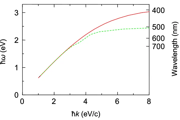
Figure 4 Dispersion diagrams of surface plasmons generated on Ag/PMMA red solid line and Au/PMMA green dotted line.
Chapter 4
Figure 1 Molecular structures for (a) pf1cnp1, (b) pf3cnp1, (c) and pftpaq.
Figure 2 PL enhancements, (a) pf1cnp1, (b) pf3cnp1, (c) pftpaq and (d) enhancement ratios plotted against the wavelength.
Figure 3 TRPL with the data normalized to 1 where the dotted line shows the conjugated polymer carrier decay rate with metal and solid line without metal, (a) pf1cnp1, (b) pf3cnp1, (c) pftpaq.
Chapter 5
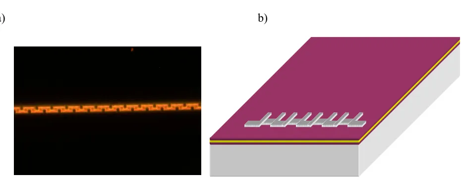
Figure 1 (a) Corrugated pattern in PMMA, on Au, on PMMA, on quartz. (b) Cartoon of layered structure, where the middle layer is the sandwiched Au between PMMA layers and an example pattern are shown.
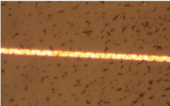
Figure 2 Fabrication steps to obtain metal-filled trenches within a sample. Figure 3 Optical microscope image of gold-filled corrugated trench in quartz. Figure 4 Corrugated wire structures at various stages of fabrication.
Figure 5 Images showing the quality of the structures.
Figure 6 Images of arrays of electron beam written patterns of different specifications. Figure 7 Images of gold corrugated lines with contact pads and cartoon of structure. Figure 8 Proposed isolated gold mounds on graphite sample schematic.
Figure 9 Mask design for making the structure and schematic of structure. Figure 10 Schematic of nanostructure sample.
Figure 11 Optical microscope image of channels in metal on quartz.
Chapter 6
Figure 1 Pump and probe beams alignments for (a) traditional optical heterodyne detected-transient grating (OHD-TG) technique and (b) the present mask pattern transferred-transient grating (MPT-TG) technique.
Figure 2 Schematic diagram of the permanent metal grating and induced spatial
and millisecond timescale (b). The dashed lines denote the initial intensities of the reference beam (Ir).
Figure 4 Semi-log plots of the TG signals in microsecond timescale (a) and in millisecond timescale (b). The straight lines are best fits.
Chapter 7
Figure 1 Illustration of nanosieve, left, and close-up on the right, with a thin gold film evaporated on both sides of the substrate. (Layers not drawn to scale.)
Figure 2 SEM view of e-beam-written, etched holes and alignment mark used for offsetting the top layer.
Figure 3 Suspended epi-Si membrane with e-beam-written holes in the center.
Chapter 8
Figure 1 Surface Plasmon Effect without nitrogen flowing.
Figure 2 Nitrogen Effect illustrating the PL intensity decay of the conjugated polymer on bare quartz with nitrogen flowing.
Figure 3 Surface Plasmon Effect and Nitrogen Effect.
Chapter 9
Figure 1 Cartoon illustration of the fabrication process for the entrenched metal grating structures.
Figure 3 Peak PL intensities of the conjugated polymer on the entrenched metal gratings fabricated.
This thesis is for my parents and all of my family and friends.
With great humility I attempt to acknowledge those that have made this thesis possible. I would like to also thank the well wishers all over the country that have met me with inspiring words with each encounter.
I am indeed thankful for the journey. In addition to what I have learned over these years, I am extremely happy for those whom I have had the opportunity to teach while a student.
Thanks to my many mentors at Morehouse College and Georgia Tech. Thanks to all the well wishers back home in GA. “Putting Warrenton on the map”. Thanks to my
collaborator extraordinaire, Dr. Koichi Okamoto. I also appreciate the discussions with colleagues and friends: Zhaoyu Zhang, Yan Chen, Sandra Steinberg, Joe Zendejas, and Dr. Christopher Boxe.
I also thank the following: NASA Ronald E. McNair for undergraduate support and internships, AT&T for a summer research experience, Undergraduate Research
I thank my collaborators at the University of Washington, Prof. Alex Jen, and Dr. Michelle Liu and the CMDITR.
Thanks to the administrators for providing the opportunity to recruit and mentor in many capacities, allowing me to maintain the “whole student” status.
We have experimentally verified that visible light emission for various organic light emitters can be enhanced through the use of surface plasmon coupling layers. By matching the plasmon frequency of a thin unpatterned silver film to the emission of a dye-doped polymer deposited onto this metal surface, we have observed an 11-fold enhancement of light emission. By patterning the silver layer, we estimate that the plasmon frequency can be tuned to match dye-doped polymer emission frequencies, and even larger emission enhancements as well as extraction efficiencies are expected. Carrier dynamics of such plasmon-enhanced organic light emitters were studied and a recombination rate increase due to surface plasmon polaritons was experimentally observed. Internal quantum efficiency data from the polyfluorenes studied follow the trend supported by the time-resolved photoluminescence measurements. Also, we have presented a way to extend the lifetime of organic light emitters by reducing the
Chapter 1–Introduction
Three areas-nanotechnology, surface plasmons, and light-emitting devices-come together
as the backbone of this thesis. Nanotechnology can be defined as the study or
manipulation of things on the order of billionths of a meter in size. In the area of light
emitting devices, the focus is drawn from vacuum tube technology to semiconductor
devices to conducting polymers. The angle taken with surface plasmons is from theory to
application. Nano-sized particles and structures are known to exhibit a strong interaction
with light. We use nanotechnology to make and modify devices, specifically to enhance
device capability. Therefore, it is not uncommon that we have a interweaving of topics in
this thesis, since on the path to achieving new landmarks in science the research efforts
are becoming more interdisciplinary. It is with that idea of pioneering areas that this
work is based.
This introduction chapter briefly outlines the work carried out in the subsequent chapters
of this thesis. The interdisciplinary nature of this thesis calls for a background of a
couple of areas that are each given adequate attention in Chapter 2. One main hurdle to
overcome when working on topics that span several disciplines is language. In the effort
detailed in this thesis, we lean more toward the applied physicist and engineering way of
looking at things when describing all the topics covered.
The work discussed in Chapter 3 has already gained attention of readers in the magazine
Laser Focus World, 1 where the work detailing surface plasmon enhanced light emission
films. Commercial laser dyes were doped into a host polymer, polymethylmethacrylate
(PMMA). Also, more intensive studies studying the size dependent photoluminescence
of silver nanoparticles doped in PMMA have been inspired by my work.2
In Chapter 4 we continue looking into the effect of emission intensity enhancements of
organic light emitters due to surface plasmons coupling to light. Having noticed the
impact of OLEDs as well as being aware of some of their high internal quantum
efficiencies, we decided that the material used to make them should be candidates for this
study. The carrier dynamics, mainly the lifetime of the carriers, are also compared.
While some researchers search for new architectures to achieved high efficiency organic
light-emitting diodes,3 others work on theoretically investigating the tuning the surface
plasmons that couple spontaneously from emitted photons to increase the efficiency of
light-emitting devices.4 Indeed, some theoretical and experimental work has been
pursued to extract more light from polymer light-emitting diodes.5 Citrin recently
published an article of interest that presents a possible theory for plasmon polaritons in
nanoparticle chains within a gain medium for the possibility of using the gain to
counterbalance dissipation and achieve low attenuation plasmon polaritons in
nanoparticle chains.6 The work by Citrin also supports the theme of the work discussed
in Chapter 3.
In Chapter 5 we revisit nanofabricated devices and their applications, which set the theme
for the research carried out in Chapters 3, 4, 6, and 7. Chapter 5 contains projects
level of expertise was attained. Most of the projects were fabrication intensive, involving
many lithography steps. However, the technology behind making the devices was
directly applicable to several areas. A nanostructured insulating substrate, as describe in
the chapter, was useful in most cases where control of the analysis of nanoparticles or
analysis performed with nanowires defined on the substrate was desired.
On the other hand, the fruit of the labor came in the form of the research topics explored
thereafter. For instance, for the work in Chapter 7 we describe a method to have dynamic
control over the size of particles filtered. Conventional methods of lithographically
defining holes for the filter size are combined with advantages from thin film depositions.
Moreover, the skills of nanofabrication were directly applicable for a new technique in
the class of optical heterodyne detected transient grating that is presented in Chapter 6.
This technique, mask pattern transferred transient grating, is a convenient new technique
to study chemical reactions and molecular dynamics. It is expected that the application
of this simpler technique is not limited to chemistry and will span other science
disciplines.
Chapters 37, 68, and 79 are published works, whereas Chapter 4 has been submitted for
publication. Chapter 5 simply consists of unpublished works.
Chapter 8 came as a result of observation made during the exploration of topics covered
in Chapters 3 and 4. In Chapter 8, we demonstrate a way to extend the lifetime of
organic light emitters by reducing the photodegredation effects from photo-oxidation
order to maximize the surface plasmon coupling. In Chapter 9, we investigate grating
structures both within and on a substrate by pholuminescence measurements of the
conjugated polymer placed on the samples. We observe emission intensity enhancements
due to surface plasmon coupling.
Last but not least, conclusions containing mainly the big picture of the accomplishments
of the work discussed are listed at the end of this thesis. Supporting materials are found
References
1. Wallace, J. “Surface plasmons boost emission from dyed polymer,” Laser Focus World, September 2005.
2. Basak, D., Karan, S., and Mallik, B., Chem. Phys. Lett. 420 (2006) 115–119.
3. Kim, H., Horwitz, J.S., Kim, W.H., Kafafi, Z.H., and Chrisey, D.B., Journal of Appl. Phys., 91, 8, 2002.
4. Paiella, R., Appl. Phys. Lett., 87, 111104 2005.
5. Ziebarth, J. M., McGehee, M.D., Journal of Appl. Phys., 97, 064502, 2005.
6. Citrin, D.S., Opt. Lett., 31, 98–100, 2006.
7. Neal, T.D., Okamoto, K., Scherer, A., Optics Express, 13, 14, 5522–5527, 2005.
8. Neal, T.D., Okamoto, K., Liu, M.S., Jen, A.K-Y, Scherer, A., Chu, C-F.,
Submitted 2006.
Surface plasmons
We commence this study by exploring the physics of surface plasmons, electromagnetic
surface waves that have their intensity maximum in the surface and exponentially
decaying fields perpendicular to it. The oscillations of the electric field encounters the
surface charge of the metal and essentially yields these trapped electromagnetic fields
between the metal and the dielectric.
Researchers have developed methods to observe1 and have intensively studied the
surface plasmon polaritons2 and examined the nature of the surface plasmon-polariton
modes and how the energy lost to the modes can be recovered when light-emission
sources are in close proximity to a thin metallic film. Also, the ability to design the
surface plasmon modes has been proposed3 and experimentally verified. 4
Dispersion Relation
The dispersion relation5 relates the frequency of surface plasma oscillations to its wave
vector. We can describe the field by
0 exp[ ( x z )]
E E= ± +i k x k z± −ωt 2.1
with + for z 0, - for z 0, and with imaginary , which causes the exponential decay of
the field . The wave vector lies parallel to the x direction;
≥ ≤ kz
z
E kx kx =2 /π λp, where λp
dispersion relation for the plane surface of a semi-infinite metal with the dielectric
function ' ''
1 1 2
(ε = +ε iε ), adjacent to a medium ε2 as air or vacuum:
1 2 0 1 2 0 z z k k D ε ε
= + = 2.2
2 2
i c kx k
ω
ε ⎛ ⎞ 2
zi
= +
⎜ ⎟
⎝ ⎠ or 2.3
1/ 2 2
2
zi i x
k k c ω ε ⎡ ⎛ ⎞ ⎤ =⎢ ⎜ ⎟ − ⎝ ⎠ ⎢ ⎥
⎣ ⎦⎥ , i=1, 2.
1/ 2 1 2 1 2 x k c ε ε ω ε ε ⎛ ⎞ = ⎜ +
⎝ ⎠⎟ 2.4
Surface plasmons (SPs) are excited by the interaction between light and metal surfaces.5-6
SPs, known to enhance absorption of light in molecules,7 increase Raman Scattering
intensities and light transparencies,8-9 and also generate photonic band gap.12-13 Since
1990, SPs have also received much attention when used in inorganic and organic light
emitters.14-23 Gianordoli et al. optimized the emission characterizations of GaAs-based
LEDs by SPs.18 Vuckovic et al. reported the SP-enhanced LED analyzing by both
theoretically and experimentally.19 Thus, great attention has been focused on SP
enhanced emission. Other avenues in this field of research became apparent when
Hobson et al. reported the SP-enhanced organic LEDs.20 For InGaN QWs, Gontijo and
co-workers report the coupling of the spontaneous emission from QW into the SP on
silver thin film and showed increased absorption of light and the SP frequency.21 Neogi
light could not be extracted efficiently from the silver/GaN surface. Therefore, the actual
photoluminescence (PL) enhancement of InGaN/GaN by coupling into SP had not been
observed directly until Okamoto and co-workers reported for the first time large PL
increases from InGaN/GaN QW material coated with metal layers.23
Conjugated polymers
The 2000 Nobel Prize in Chemistry was awarded to Alan J. Heeger, Alan G. MacDiarmid,
and Hideki Shirakawa for work on polyacetylene, an organic polymer that can be
converted to a conducting polymer. Since that discovery, a tremendous amount of work
has been done on conjugated polymers, because of their ability to exhibit high
conductivity when doped. A conjugated polymer is a carbon-based macromolecule
through which valence π-electrons are delocalized. The electronics industry finds a
particular interest in conjugated polymers for their electronic, optical, and mechanical
properties as well as the intrinsic processing advantages that makes room for a wide array
of applications, including but not limited to light-emitting devices, photovoltaic devices,
electromagnetic shielding, plastic field-effect transistors, and nonlinear optical devices.24
Some structural studies25 represent some of the challenges that one encounters when
attempting to understand the physical properties of such polymers. Many opportunities
already exist for electrically conductive organic polymers, as studies26 have been done to
identify strong candidates for spacecraft materials, in reference to the thermal stability,
radiation resistance, and strength of the polymer. Still there is much to find out about the
Researchers find it possible to understand the polymer properties further by using time
resolved photoluminescence studies to characterize conjugated polymers.27,28
Quite an effort has been place in the efficiencies and electron transporting properties of
1. Giannattasio, A., Barnes, W.L., Optics Express, 13, 2, 2005
2. Wedge, S., Barnes, W.L., Optics Express, Vol. 12, No. 16, 2004
3. Pendry, J.B., Martin-Moreno, L., Garcia-Vidal, F.J., Science 305, 847, 2005.
4. Hibbins, A.P., Evans, B.R., Sambles, J.R., Science, 308, 670, 2005.
5. Raether, H., Surface plasmon on smooth and rough surfaces and on grating, Springer, Berlin, 1988.
6. Liebsch, A., Electronic Excitations at Metal Surfaces, Physics of Solids and Liquids, Ansgar, Libsch, 1997.
7. Ford, G.W., and Weber, W.H., “Electromagnetic-interactions of molecules with metal-surfaces,” Phys. Rep. 113, 195–287, 1984.
8. Fleischmann, M., Hendra, P.J., and McQuillan, A. J., “Raman spectra of pyridine adsorbed at a silver electrode,” Chem. Phys. Lett. 26, 163–166, 1974.
9. Garcia-Vidal, J.F., and Pendry, J.B., “Collective theory for surface enhanced Raman scattering,” Phys. Rev. Lett. 77, 1163–1166, 1996.
10. Ebbesen, T.W., Lezec, H.J., Ghasemi, H.F., Thio, T., and Wolff, P.A.,
“Extraordinary optical transmission through sub-wavelength hole arrays,” Nature, 391, 667–669, 1998.
11. Schroter, U., and Heitmann, D., “Surface-plasmon-enhanced transmission through metallic gratings,” Phys. Rev. B, 58, 15419–15421, 1998.
12. Kitson, S.C., Barnes W.L., and Sambles, J.R.A., “Full photonic band gap for surface modes in the visible,” Phys. Rev. Lett. 77, 2670–2673, 1996.
13. Barnes, W.T., Preist, T.W., Kitson, S.C., and Sambles, J.R., “Physical origin of photonic energy gap in the propagation of surface plasmon on grating,” Phys. Rev. B. 54, 6227–6244, 1996.
14. Kock, A., Gornik, E., Hauser, M., and Beinstingl, M., “Strongly directional emission from AlGasAs/GaAs light-emitting diode,” Appl. Phys. Lett. 57, 2327–2329, 1990.
16. Hecker, N.E., Hopfel, R.A., and Sawaki, N., Maier, T., Strasser, G., “Surface plasmon-enhanced photoluminescence from a single quantum well,” Appl. Phys. Lett. 75, 1577–1579, 1999.
17. Barnes, W.L., “Electromagnetic crystals for surface plasmon polaritons and the extraction of light from emissive devices,” J. Light. Tech., 17, 2170–2182, 1999.
18. Gianordoli, S., Hainberger, R., Kock, A., Finger, N., Gornik, E., Hank, C., and Korte, L., “Optimization of the emission characteristics of light emitting diodes by
surface plasmons and surface waveguide modes,” Appl. Phys. Lett. 77, 2295–2297, 2000.
19. Vuckovic, J., Loncar, M., Scherer, A., “Surface plasmon enhanced light-emitting diode,” IEEE J. Quant. Elec. 36, 1131–1144, 2000.
20. Hobson, P.A., Wedge, S., Wasey, J.A.E., Sage, I., and Barnes, W.L., “Surface plasmon mediated emission from organic light emitting diodes,” Advanced Materials, 14, 1393–1396, 2002.
21. Gontijo, I., Borodisky, M., Yablonovitch, E., Keller, S., Mishra, U.K., DenBaars, S.P., “Enhancement of spontaneous recombination rate in a quantum well by resonant surface plasmon coupling,” Phys. Rev. B, 60, 11564–11567, 1999.
22. Neogi, A., Lee, C.-W, Everitt, H.O., Kuroda, T., Tackeuchi, A., Yablonovitch, E., “Enhancement of spontaneous recombination rate in a quantum well by resonant surface plasmon coupling,” 66, 153305, 2002.
23. Okamoto, K., Niki, I., Shvartser, A., Narukawa, Y., Mukai, T., Scherer, A., “Surface-plasmon-enhanced light emitters based on InGaN quantum wells,” Nature Mater., 3, 601–605, 2004.
23. Barford, W., Electronic and optical properties of conjugated polymers, Oxford University Press Inc., New York, 2005.
24. Pouget, J.P., Robin, P. Comes, R., Gibson, H.W., Epstein, A.J., Billaud, D., Physica, 127 B, 158, 1984.
25. Cotts, D. B., and Reyes, Z., “Electrically conductive organic polymers for advanced applications,” Noyes Data Corporation, New Jersey 1986.
26. Whitelegg, S.A., Buckley, A., Rahn, M.D., Fox, A.M., Bradley, D.D.C., Palsson, L.O., Samuel, I.D.W., Webster, G.R., Burn, P.L., Synthetic Metals, 119, 575–576, 2001.
29. C-F. Shu, R. Dodda, F-I. Wu, M. S. Liu, and A. K-Y. Jen, Macromolecules, 36, 6698–6703, 2003.
Chapter 3–Surface plasmon-enhanced emission from
dye-doped polymer layers
Abstract: We have experimentally verified that the emission of visible light from
dye-doped polymers can be enhanced with the use of surface plasmon coupling. By matching
the plasmon frequency of a thin unpatterned silver film to the emission of a dye-doped
polymer deposited onto this metal surface, we have observed an eleven-fold enhancement
of light emission. By patterning the silver layer, we estimate that the plasmon frequency
can be tuned to match dye-doped polymer emission frequencies, and even larger emission
The large optical fields provided by surface plasmons have in the past been used to
increase significantly the fluorescence and luminescence intensity of dye molecules for
applications in biological and biochemical sensing. Molecules can be detected on the
surface of metal films or in close proximity to colloidal metal particles by measuring
increases in the resonant surface plasmon coupled emission.1 Recently, it has also been
shown that plasmon resonances provided by thin metal layers and metal gratings can be
designed to increase the efficiency of solid state semiconductor light sources. In such
structures, the surface plasmon resonance frequency is tuned to the semiconductor
quantum well emission, and the light-emission intensity can be increased by over an
order of magnitude as nonradiative recombination paths are bypassed through coupling of
recombination energy into surface plasmon modes. It is therefore not surprising that
similar energy transfer into surface plasmons can also be exploited in the design of more
efficient organic light emitters. Recently, the mechanism for emission enhancement
through coupling to surface plasmons has been analyzed for InGaN quantum wells.2
Other enhancement efforts to increase the external quantum efficiencies and increasing
the spontaneous emission rates, using surface plasmons, have been reported for
semiconductor quantum wells.3-6 Similar increases in the internal and external quantum
efficiencies to those observed in InGaN quantum wells in close proximity to metal
surfaces can be obtained from dye-doped organic thin films.
Polymers, appropriately doped with dye molecules, emitting in the visible spectrum
provide stable sources of light for displays and illumination sources at a significantly
evolve as the most inexpensive alternatives to fluorescent light sources for large area
solid state lighting. Thus, it is of both commercial and scientific interest to improve the
internal quantum efficiencies of the polymer dyes within such light emitters, as well as to
increase the light extraction efficiencies from such organic films. Indeed, the effect of
surface plasmons on the light emission from polymer layers has recently been
investigated by several groups.9-11 Nanosensors using surface plasmon resonance as well
as their applications in conjunction with dye-doped polymers or polymer thin films have
also been explored.12-14 Here, we focus on enhancing the light emission efficiency from
organic thin films by using the surface plasmon resonance.
Experiment
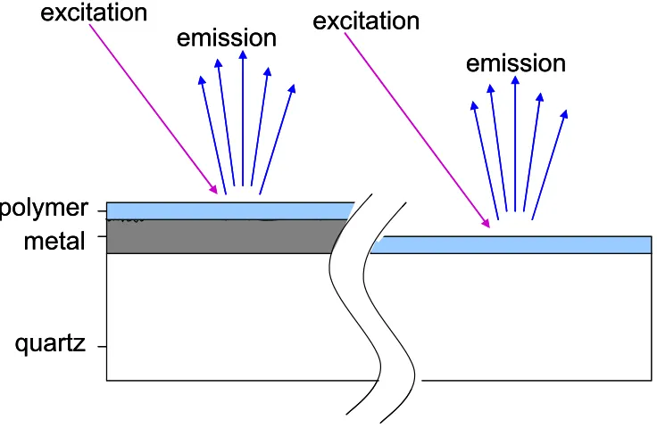
The experimental setup used to measure our samples is shown in Fig. 1. To ensure that
only a small amount of the pump light is reflected into the detector, the pump source is
introduced at a large incidence angle while the detector is located perpendicular to the
sample. We employ an Ocean Optics spectrometer to measure the emission intensity of
the organic dye layers. We compare the influence of gold and silver thin films on the
light emission of a commonly used laser dye doped in a polymer by using this
measurement system. Of course, the light-emitting material must be within a few hundred
nanometers of the metal surface to benefit from surface plasmon enhancements. For
semiconductor quantum wells, this is normally accomplished by growing a very thin
spacer separating the quantum well from the metal surface. For polymer layers, it is
much simpler to prepare measurable samples, as it is only necessary to ensure that the
polymer
quartz
metal
excitation
excitation
emission
emission
polymer
quartz
metal
excitation
excitation
emission
emission
Fig. 1. Sample structure with both pump light and emission light configurations.
measurements conducted on semiconductor emitters have concentrated on backside
pumping, through the sample, with the emission light measured also from the backside of
the sample.2 Some other work has measured the optical properties of semiconductors by
topside pumping, through the metal, and measuring also from the top side.4,5
Combinations of the different pumping and measurement configurations, as well as
different angles for the pumped light, have also been pursued.6 For this paper, it is most
convenient to pump through the polymer as well as measure light from the polymer side
It is of interest to control both the concentration of the dye material in the polymer as
well as the thickness of the polymer. Dye polymer solution was prepared by dissolving
common laser dye molecules of Coumarin 460 in chlorobenzene. This laser dye emits
blue light at 460 nm with UV excitation. Then 2% polymethylmethacrylate (PMMA)
was added to the mixture as a host matrix to obtain a 20 mM/L solution of the dye doped
polymer solution. Photoluminescence measurements were performed by using a 405 nm
InGaN laser diode to pump the Coumarin 460 dye. For the 405 nm pump light in
Coumarin 460 the absorbance is 0.633[10-4 dm3mol-1cm-1]. Our concentration of 2.16 x
10-2 moles/L therefore results in an approximate excitation light penetration depth of
~646 µm, a penetration depth much larger than the sample thickness of 200 nm. To
prepare the substrates for the dye-doped layers, 50 nm thick silver and gold layers were
vapor deposited onto quartz substrates at 0.5 nm/second deposition rates. Gold and silver
layers prepared under these conditions exhibit surface roughness of 30–40 nm resulting
from the crystal size of the metal layers.2 Only half of each substrate was metallized,
enabling the rapid comparison between polymer emission on top of metal layers with
polymer deposited on quartz. After the metallization step, the dye doped PMMA layers
no metal
Au
Ag
400
500
600
0
5
10
Wavelength (nm)
PL Int
ensit
y (a.
u.)
no metal
Au
Ag
400
500
600
0
5
10
Wavelength (nm)
PL Int
ensit
y (a.
u.)
Fig. 2. PL spectra of Coumarin 460 on Ag, Au, and on no metal. Coumarin 460 PL
Results and Discussion
Figure 2 shows a typical measurement obtained when comparing the spectra of a region
with Coumarin 460-doped PMMA spun onto gold with that of the polymer on the bare
quartz substrate. While the gold assisted in reflecting the pump laser, the surface
plasmons did not seem to couple to the emission wavelength of Coumarin 460 to offer
any measurable enhancement. However, we do observe an 11-fold enhancement of the
emission light from the Coumarin-doped PMMA on silver due the coupling of the surface
plasmons generated on the silver film as the plasmon resonance frequency closely
matches the emission frequency of the dye. Indeed, the dielectric constants for silver
match well with the emission wavelength of Coumarin 460, and the data with the
Coumarin 460 PL intensity is normalized to 1. While reflection can be used to account
for some of the increased brightness, only the SP coupling can explain the enhancement
450
500
550
600
0
10
20
30
40
Wavelength (nm)
P
L-E
nha
nc
em
ent
Rat
io
450
500
550
600
0
10
20
30
40
Wavelength (nm)
P
L-E
nha
nc
em
ent
Rat
io
Fig. 3. PL Enhancement ratios demonstrating an increase of enhancement with shorter
wavelengths using the silver film. Green dotted line is for gold whereas red solid line is
Enhancement ratios illustrated in Fig. 3 further support the notion of SP coupling
between the silver and polymer interface. Up to 50 times the enhancement is observed
along the broad emission spectrum of the dye-doped polymer whereas at the peak
emission wavelength the photoluminescence enhancement ratio is 11 times. We
observed an increase of photoluminescence enhancement ratio with shorter wavelengths
for the silver film. However, the PL enhancement ratio is not strongly dependent on the
change in wavelength for the gold film.
The dramatic PL enhancement of samples with Ag can be attributed to the strong
interaction between the excited dye molecules and SPs. Electron-excited energy of
molecules can couple to the electron vibration energy of SP. Then, the molecular
relaxation processes may produce an SP instead of a photon, and this new path of the
relaxation increases the spontaneous recombination rate. If the metal surface were
perfectly flat, it would be difficult to extract light emission from the SP, since it is a
non-propagating evanescent wave. However, roughness and imperfections in evaporated
metal can scatter SPs as light. The coupling rate between the excited molecular and SP is
expected to be much faster than the nonradiative relaxation processes as a result of the
large electromagnetic fields introduced by the large density of states.
The phenomenon we exploit here heavily depends on the relationship of the metal
dielectric function15 and that of the polymer. The dielectric constant for PMMA is 2.6 at
1 MHz. The surface plasmon dispersion relationship is obtained by using the following
equation to calculate the propagation wave number k:
2 1 2 1 ε ε ε ε ω + = c
constant of metal and PMMA, respectively. In this equation, the wave number k varies
with frequency ω. The plot of the surface plasmon dispersion relationship in Fig. 4 is
calculated using Eq. (1).
ħ
k
(eV/c)
ħ
ω
(eV
)
0
2
4
6
8
0
1
2
3
400
500
600
700
Wa
ve
le
ng
th
(nm)
ħ
k
(eV/c)
ħ
ω
(eV
)
0
2
4
6
8
0
1
2
3
400
500
600
700
Wa
ve
le
ng
th
(nm)
Fig. 4. Dispersion diagrams of surface plasmons generated on Ag/PMMA red solid line
and Au/PMMA green dotted line.
The asymptotes of the Ag/PMMA and Au/PMMA surface plasmon dispersion curves
closely approach the surface plasmon frequency for silver and gold, respectively. We can
therefore determine the energy due to the coupling at the interface of the metal and the
polymer. This provides a further explanation for the energy coupling exhibited in the
laser dye-doped polymer deposited on different metallized substrates. Emission of the
Usually, surface plasmons generated at the interface of the metal and the surrounding
medium decay exponentially with distance from the metal surface. We can predict the
surface plasmon penetration depth (Z) in the polymer from the following equation:
2
1 1 2
2 ε
ε ε π
λ −
=
Z (2)
This penetration depth is 38.6 nm for silver and 23.0 nm for gold, when we substitute
the wavelength of the pump light λ. Therefore, since our penetration depth in the
polymer due to the excitation wavelength and concentration of the dye molecules in the
polymer was much longer than the penetration depths of the surface plasmons in the
polymer, we could excite every part of the dye molecules adjacent to the metal.
Spacer dependency was explored by fabricating a new sample and first spinning on a
50 nm thick non-doped polymer layer and baking it at 180 °C to drive off the solvents.
This layer was sandwiched between the metal film and the dye-doped polymer layer and
lowered the coupling efficiency by not allowing efficient enhancement due to surface
plasmons. This configuration placed the light-emitting material much farther away from
the metal than the surface plasmon penetration depth mentioned above. Metal
dependency trials performed showed that a thinner gold film, around 10 nm, had
enhanced absorption while a thinner silver film, also 10 nm, did not enhance the signal.
We have observed that the emission of dye-doped polymers can be enhanced by using
surface plasmon coupling to thin metal layers. This study serves as a foundation for the
geometric tuning of the surface plasmon resonance and enhancement of the emission of
dye polymers using surface plasmons with patterned metal samples. If tuned properly,
such lithographically structured layers should provide even higher enhancement values
for the dye emission intensity. As the metallic surface can be used as an electrical
contact, as a metallic grating for enhanced light extraction, and as a mirror for the
definition of ultra-small optical cavities to further increase the spontaneous emission
rates, we expect that many organic light-emitting diodes could benefit from careful
design and choice of metallization. Ultimately, lithographic tuning of the peak emission
wavelength and optimization of the polymer layer stack can also result in efficient white
References
1Malicka, J., et al., “Use of surface plasmon-coupled emission to measure DNA
hybridization,” J. Biomol. Screening, 9, 208–215, 2004.
2Okamoto, K., et al., "Surface-plasmon-enhanced light emitters based on InGaN quantum
wells," Nature Materials, 3, 601–605 2004.
3Vuckovic, J., M. Loncar, and A. Scherer, "Surface plasmon enhanced light-emitting
diode," IEEE J. Quantum Electronics, 36, 1131–1144, 2000.
4Gontijo, I., et al., "Coupling of InGaN quantum-well photoluminescence to silver
surface plasmons," Phys. Rev. B, 60, 11564–11567, 1999.
5Neogi, A., et al., "Enhancement of spontaneous recombination rate in a quantum well by
resonant surface plasmon coupling," Phys. Rev. B, 66, 2002.
6Hecker, N.E., et al., "Surface plasmon-enhanced photoluminescence from a single
quantum well," Appl. Phys. Lett, 75, 1577–1579, 1999.
7Jiang, X.Z., et al., "Organic light-emitting diodes using an in situ thermally polymerized
hole transporting layer," Appl. Phys. Lett., 76, 2985–2987, 2000.
8Carlson, B., et al., "Divalent osmium complexes: Synthesis, characterization, strong red
phosphorescence, and electrophosphorescence," J. Am. Chem. Soc., 124, 14162–14172, 2002.
9Hobson, P.A., et al., "Surface plasmon mediated emission from organic light-emitting
diodes," Advanced Materials, 14, 1393–1396, 2002.
10Andrew, P. and W.L. Barnes, "Energy transfer across a metal film mediated by surface
plasmon polaritons," Science, 306, 1002–1005, 2004.
11Alencar, M., A.S.L. Gomes, and C.B. de Araujo, "Directional laserlike emission from a
dye-doped polymer containing rutile nanoparticles," J. Opt. Soc. Am. B-Optical Physics, 20, 564–567, 2003.
12Uznanski, P. and J. Pecherz, "Surface plasmon resonance of azobenzene-incorporated
polyelectrolyte thin films as an H+ indicator," J. Appl. Polymer Sci., 86, 1459–1464, 2002.
13Tawa, K. and W. Knoll, "Out-of-plane photoreorientation of azo dyes in polymer thin
15Carper, J., The CRC Handbook of Chemistry and Physics, Library Journal, 124, 192–+,
Chapter 4–Time-resolved photoluminescence spectroscopy of
surface plasmon-enhanced light emission from conjugate
polymers
Abstract
We have experimentally verified that the light emission from conjugated polymers can be
enhanced through the use of surface plasmon coupling layers. Carrier dynamics of such
plasmon-enhanced organic light emitters were studied and a recombination rate increase
due to surface plasmon polaritons was experimentally observed. Internal quantum
efficiency data from the polyfluorenes studied follow the trend supported by the
Introduction
Organic light-emitting diodes (OLEDs) have become widely available and are
used for replacing inorganic light-emitting diodes, as they are less expensive and provide
many opportunities in regards to structural placement. Despite the tremendous promise
for efficient solid state lighting offered by such organic light emitters, the road towards
spectrally broad white light polymer emitters still holds many design challenges.
Enhancement methods for efficient light emission have been studied for several inorganic
semiconductors, and one very effective approach to developing highly efficient light
emitters has been based on the incorporation of metals for the efficient extraction of light.
Recently, we reported dramatic enhancements of the light emission from inorganic1,2 and
organic3 light emitters using surface plasmon coupling. These can now be applied
towards OLED material and incorporated together with advances in polymer chemistry
that have recently resulted from the addition of fluorine-based polymers or phosphors.4,5
Experiment
Here we focus on increasing the light-emission efficiency from optimized blue
light-emitting polymers through the use of surface plasmons for enhancement of the
internal quantum efficiency. Three conjugated polymers were studied: PF-CNP (1:1),
PF-CNP (3:1), and PF-TPA-Q. The molecular structures for the conjugated polymers
used are illustrated in Figure 1.7,8 The corresponding conjugated polymers PF-CNP (1:1),
PF-CNP (3:1), and PF-TPA-Q will be referred to as pf1cnp1, pf3cnp1, and pftpaq,
C6H13 C6H13
CN
NC
1 C6H13 C6H13 C6H13 C6H13
3 1
a)
C6H13 C6H13
CN
NC
1 C6H13 C6H13 C6H13 C6H13
3 b)
N N
C8H17C8H17
C8H17
C8H17
N N
n-Bu n-Bu
n-Bu
n n
n-Bu c)
had previously been coated with a 50 nm silver layer. Photoluminescence measurements
were then performed to compare the different areas of the sample, comparing the
luminescence efficiency from emitters with no metal with those in proximity to the metal.
Similar to Chapter 3,3 the sample geometry consists of quartz samples covered
with silver and light emitting polymer layers. In this Chapter, however, conjugated
polymers are used instead of a dye-doped polymer films, and we present new
photoluminescence results on these much more efficient emitter materials, in which the
fluorophore concentration is higher compared to laser dyes doped within a polymer
matrix. More interesting observations are possible with such efficient polymer emitters.
The experimental setup and measurements for detecting emission intensity
enhancements is described in our previous work3 on enhanced emission from dye-doped
polymer layers. An InGaN 405 nm diode laser was used to excite the samples. A
Princeton Instruments Cooled CCD and Acton Research Corporation Spectrograph were
used to perform measurements of the emission intensities of these samples. Moreover, a
Hamamatsu Photonics streak camera was used to obtain time-resolved
photoluminescence (TRPL) spectroscopy data from polyfluorene emission rates after
deposition on silver coated quartz samples. For the TRPL measurements, a frequency
doubled beam of a mode-locked Ti sapphire laser (Spectra Physics) was used to excite
the samples. The pulse width, wavelength, and repetition rate were chosen as 100 fs, 400
nm, and 80 MHz, respectively. These TRPL studies determined decay rates at various
wavelengths, as well as the Purcell6 factors. Carrier dynamic measurements were
and confirm that some conjugate polymers are better suited for luminescence
enhancement resulting from coupling to surface plasmons. A neutral density filter was
added in the setup just before the detector as the signal intensities were significantly
larger than from our previous dye-doped polymer work. By employing the use of a
shutter, photo-oxidation of these somewhat unstable conjugated polymers could be
largely avoided.
450 500 550 600 0
1 2
3 pf1cnp1
3 times enhancement
P L I nt en si ty ( a.u.) Wavelength (nm)
a) b)
450 500 550 600 0
1 2
3 pf3cnp13.2 times enhancement
P L I nt ens it y ( a.u .) Wavelength (nm)
c) d)
450 500 550 600 0 1 2 3 4 5 pftpaq
4.4 times enhancement
P L I nte nsity ( a. u. )
Wavelength (nm) 400 500 600
1 2 3 4
pf1cnp1 line pf3cnp1 dashed line pftpaq dotted line
Wavelength (nm) PL en ha ncemen t rat io (a.u .)
0 1 2 0 0.2 0.4 0.6 0.8 1 pf1cnp1 line no metal dotted metal Time (ns) PL in te ns it y ( a.u .)
0 1 2
0 0.2 0.4 0.6 0.8 1 pf3cnp1 line no metal dotted metal Time (ns) P L inte nsity ( a. u. )
a) b)
c)
0 1 2
0 0.2 0.4 0.6 0.8 1 pftpaq line no metal dotted metal Time (ns) PL in te ns it y (a .u .)
Results and Discussion
The enhancements observed for pf1cnp1, pf3cnp1, pftpaq, were 3, 3.2, and 4.4
times, respectively, and are shown in Figures 2a–c. In Figure 2d the enhancement ratios
for each conjugated polymer reflect a maximum enhancement for shorter wavelengths. A
larger contribution due to the surface plasmon coupling is evident, as shorter wavelengths
have higher enhancements. This finding can be explained by the surface plasmon
dispersion diagram, which indicates a better match between the silver plasmon resonance
and the emission at shorter wavelengths.3
Figure 3 compares the time-resolved PL decay profiles between the conjugated
polymers deposited on quartz and on silver films on quartz sample. Longer PL lifetimes
were measured for the conjugated polymer on bare quartz. The observation of a faster
decay profile for pf1cnp1 on metal on quartz suggested that there was significant transfer
of energy between the conjugated polymer and the silver surface plasmon polariton.
Conjugated polymers with bipolar charge-transporting properties, namely pf3cnp1 and
pftpaq, already exhibited fast decay rates without the silver layers and therefore the
lifetime is similar to that when surface plasmons are coupled, in turn providing no
significant reduction in the PL lifetime, τPL. However, for the better electron transporter
pf1cnp1, energy transfer is facilitated to the surface plasmons and results in shorter PL
lifetimes.
The internal quantum efficiency,ηint, is described as the radiative recombination rate
divided by the sum of the radiative, , and nonradiative recombination rates, , as
shown below.
rad
rad nonrad
where the PL lifetime is the inverse of the recombination rate, (i.e., 1 rad nonrad PL
k k
τ = + ).
For the surface plasmon case, the enhanced efficiency, * int
η , is better described by the
sum of the recombination rates that are radiative and due to surface plasmons, ksp,
divided by the sum of the radiative, nonradiative, and surface plasmon recombination
rates, as listed below. 1,2
* int
rad sp
rad nonrad sp
k k
k k k
η = +
+ +
If initially the efficiency is high, the influence from the surface plasmons is not
significant. The coupling due to surface plasmons can become very significant when the
initial quantum efficiency is low.
In Figures 4a–c, the photoluminescence lifetimes are plotted versus the emission
wavelengths. Carrier lifetimes are shorter for the case when the conjugated polymer was
deposited on the metal films. In Figure 4d, we also plot the calculated Purcell factors
versus emission wavelengths for the three conjugated polymers. These Purcell factors
represent the average of several measurements taken for each conjugated polymer.
Again, the pf1cnp1 sample showed the greatest influence on the metal surface. When the
initial lifetime was short, coupling into surface plasmons did not significantly decrease
the lifetime. For the case when the initial lifetime was long, however, surface plasmons
could substantially decrease the lifetime and increase the quantum efficiency.
Taking an in-depth look at the properties of the polyfluorenes studied can reveal
to better charge injection and more efficient charge recombination was reported by Shu
for PF-TPA-Q.8 Liu et al. extensively studied such properties of the PF-CNP (3:1) and
a) b)
420 440 460 480 0 0.05 0.1 0.15 Wavelength (nm) PL lif etim e (n s) pf3cnp1 line no metal dash metal
420 440 460 480 0 0.1 0.2 0.3 PL li fe ti m e ( ns) Wavelength (nm) pf1cnp1 line no metal dash metal
c) d)
420 440 460 480 0 0.02 0.04 0.06 0.08 0.1 PL lif etim e ( ns) Wavelength (nm) pftpaq line no metal dash metal
4200 440 460 480 1
2 solid line pf1cnp1 dashed line pf3cnp1 dotted line pftpaq
Pu rc ell f ac tor Wavelength (nm)
respectively.7 They also attributed the slow electron motion to the higher content of
cyano constituents that stabilize the radical anion and to the less planar structure of
PF-CNP (1:1). For these reasons, we expect the surface plasmon polaritons to assist in the
movement of these electrons, coupling enough energy to increase electron transport.
Some enhancement due to the coupling of surface plasmons was evident in the PL data
obtained from the metal side. These enhancements, however, were not as significant as
for the dye-doped polymer layers. We attribute this observation to the notion that the
efficiencies of the conjugated polymers are already high and we expect the coupling due
to surface plasmons to have a smaller effect on the enhancement in this case.
Conclusion
From studying the TRPL of these polyfluorenes in conjunction with the PL
enhancement ratios we have found that those with longer carrier lifetimes offer large
improvements in quantum efficiency if surface plasmons are used to enhance
recombination of electron-hole pairs. Although only 3 or 4 times emission enhancements
are observed this is a significant increase in quantum efficiency from these
state-of-the-art organic light emitters. We expect that, along with the development of robust and
efficient polymers, the use of surface plasmons will ultimately lead to highly efficient
References
1K. Okamoto, I. Niki, A. Scherer, Y. Narukawa, T. Mukai, and Y. Kawakami, Applied
Physics Letters, 87, 071102, 2005.
2K. Okamoto, I. Niki, A. Shvartser, Y. Narukawa, T. Mukai, and A. Scherer, Nat. Mater.
3, 601, 2004.
3T. D. Neal, K. Okamoto, and A. Scherer, Optics Express 13, 14, 5522–5527, 2005.
4F. Hide, P. Kozodoy, S. P. DenBaars, and A. J. Heeger, Appl Phys. Lett. 70, 20, 1997.
5C. Zhang and A. J. Heeger, Journal of Appl. Phys., 84, 3, 1998.
6E. M. Purcell, Phys. Rev. 69, 681, 1946.
7M. S. Liu, X. Jiang, P. Herguth, and A. K-Y. Jen, Chem. Mater., 13, 3820–3822, 2001.
8C-F. Shu, R. Dodda, F-I. Wu, M. S. Liu, and A. K-Y. Jen, Macromolecules, 36, 6698–
Unifying summary
A great deal of interest during my thesis work came from nanotechnology in many areas.
Some areas related to microfluidics and others to nanophotonics. The general underlying
theme was that nanofabrication tools were used and the idea of miniaturizing things and
taking advantage of the physics involved brought all of this work together. Light
manipulation remained a common thread in the majority of the work included in this
Chapter 5–Nanofabricated devices and applications
There has been some interest in fabricated structures on insulating materials,
especially when the desire is to have a substrate that does not interfere with electrical
measurement and when a thin insulating layer on the substrate is not enough. With UV
lithography, structures a few microns in size and a little smaller are possible. However,
when wanting to get sub-micron features, one would have to turn to electron beam
lithography and then find it somewhat challenging since the insulator does not conduct
and is not allowed to dissipate the charges thereby having a state of charging up on the
surface. Therefore researchers turned to imprint lithography. The technology
nano-imprint1-2 lithography has been demonstrated for grating-type structures where the
geometry is on the order of tens of nanometers, but requires an electron beam written
mold.
Here experimental results are presented on nanostructures fabricated on insulating
materials with a method that will allow complex structures to be made without using a
mold but instead using mask layers. The device proposed, not to be described but only
mentioned, is an electromagnetic trap.
Experimental procedures
In this procedure we used a fused quartz slide and prepared it with a sacrificial layer by
applying 130 nm of polymethylmethacrylate (PMMA) and baking it for 20 minutes at
180° C. Since sub-micron patterns were desired on an insulating substrate we applied a
100 nm Au film by thermal evaporation to prevent charging on the surface during
used to figure out the optimum thickness. In searching for an optimum thickness, the
chosen dose level with a 100 kV beam would yield a nice pattern with a 100 nm Au film,
which provided sufficient material for conductivity. Then PMMA was again applied this
time as the layer for electron beam writing with the same specification as above. The
Lieca EBPG was used to obtain the 100 kV beam for electron beam writing. Upon
developing of a 30 kV converted SEM beam-written pattern, the following image was
obtained, shown as Fig 1a.
a) b)
Figure 1 a) Corrugated pattern in PMMA, on Au, on PMMA, on quartz. b) Cartoon of
layered structure, where the middle layer is the sandwiched Au between PMMA layers,
and an example pattern are shown.
Calibration beam-written samples were done first using silicon and silicon on
insulator samples. The fabrication steps for those samples are shown in Figure 2.
microelectromagnetic trap
fabrication
Evaporate
100nm Au layer
Silicon/
SOI
XeF2
etch
Developing
200nm
PMMA
layer
After lift-off
Figure 2 Fabrication steps to obtain metal filled trenches within a sample.
Next a series of etching techniques were undertaken. For pattern transfer, an
argon plasma was used to mill through the 100 nm of Au, using the top layer of PMMA
as a mask. Given that the desire was to etch the underlying quartz, the bottom layer of
PMMA in the patterned region had to be removed before the SiO2 etch. By using oxygen
and argon plasma this challenge was accomplished for the 130 nm PMMA film. The etch
Following this procedure, the etched pattern was filled with gold, and what
remained of the Au sandwiched within PMMA layers was removed with acetone as
shown in Fig 3.
Figure 3 Optical microscope image of gold-filled corrugated trench in quartz.
Results and discussion
In the initial stages of this work, a scratch on the substrate was used to go from
the macro world to the microelectromagnetic trap. This scratch would remove PMMA
such that when evaporation was done the metal filling the void would be large enough for
aligning a probe tip for electrical contact. Otherwise, another optimal way to accomplish
contact would have been to add a UV lithography step after the first lift-off to align
contact pads. The use of the EBPG, electron beam pattern generator, allowed for
lithographically defining the small trap structures while also making the contact pads
After Beam writing After Lift-off
Close optical microscope image Close optical microscope image
5µm 5µm
~0.8µm
Figure 4 Corrugated wire structures at various stages of fabrication.
120%
80% 800nm gap= 100%
Dark field image after ion milling Optical microscope
images after lift-off 800nm gap
Bright Field Image Dark Field Image
800 nm box
640 nm box
480 nm box
Line (1.6 µm)
Line (1.28 µm)
Line (0.96 µm)
Actual box size is slightly smaller than the designed box.
Metal Nanostructure on Insulating Material
Geometry’s influence on the plasmon resonance
Au 100 nm PMMA 200 nm PMMA 200 nm
Quartz substrate 1 mm
100% 80% 60% 40%
10% 20%
Where 100% corresponds to 800 nm sized boxes
DNA Conductivity
In this project we seek to perform a direct measurement of DNA’s conductivity in
solution. Several samples with evenly distributed gold pads were fabricated for analysis
purposes. One convention was using an array of circles of 100 nm spaced by 5 um.
Another convention was using sub-100nm lines spaced by 100 nm.
Gold or Silver disks
Figure 8 Proposed isolated gold mounds on graphite sample schematic.
Figure 9 Mask design for making the structure and schematic of structure. Defining thickness
Oxide layer Bottom Au layer
•
Layer 0 Au pattern•
Layer 1 oxide pattern•
Layer 2 etch pattern•
Layer 3 Au patternTop Au layer
(diameter 1000–1500 A, height 50–150 A)
~500 nm
Graphite
Nanostructured insulator for metal nanoparticle analysis device
The goal of this project involved making a device for nanoparticle analysis. Silver
nanoparticles around 10 nm in size and less were coated with a polymer shell with the
intention of aligning them on a substrate such that they could be placed in a single row.
Advantages one would obtain from using the small particles would be 1) the particles,
with their small size, could be easily combined with other existing devices, 2) in solution
the particles could be easily spun onto a substrate, and (one of the main reasons) 3) the
electromagnetic field of such small particles exceeds the diameter of the particle, which
lends itself to near field interaction.
<10 nm metal nanoparticles in a 10 nm width, 10 nm depth channel, 500 um long
Figure 10 Schematic of nanostructure sample.
Quartz substrate
Figure 11 Optical microscope image of
Conclusion
Sub-100 nm structures were fabricated in an insulating material without the use of
nano-imprint lithography simply by using a combination of metal and polymer sacrificial
layers. Further studies will make use of these structures for analysis of nanoparticles or
1 M. D. Austin, S. Y. Chou, Appl. Phys. Lett. 81, 4431 (2002)
2 H. Cao, Z. Yu, J. Wang, J. O. Tegenfeldt, R. H. Austin, E. Chen, W. Wu, W. Y.
Chapter 6–Molecular dynamics study of photochromic
molecules probed by the mask pattern transferred-transient
grating technique
Abstract
Mask pattern transferred-transient grating (MPT-TG), which is a convenient new
technique in the class of optical heterodyne detected-transient grating (OHD-TG), is
applied to photochromic molecule (spiropyran) in 2-propanol solution. The spatial
modulation of optical properties of the material is generated by transferring an
ultra-violet light pattern directly from a metal film grating into the sample solution and
detected through the diffraction of a probe beam. The thermal conductivity of the solvent
and the diffusion coefficients of the solute molecules were obtained and compared with
the calculated values. This method has many advantages compared to the conventional
The transient grating (TG) technique, which is one of the third order
nonlinear spectroscopies, has been a useful and powerful tool for studies in photonics and
in photochemical processes of solutions.1-6 This technique has many unique advantages.
For example, it is capable of monitoring molecular dynamics of short-lived chemical
species in solutions.7-10 However, there are several difficulties in this technique. The
diffracted signal intensity (ITG) is given by the sum of the square of refractive index
change (δn; phase grating) and absorbance change (δk; amplitude grating) induced by the
optical interference pattern. The quadratic nature of the signal intensity makes the
analysis of the signal components complicated. Also, contributions of the phase and
amplitude gratings are difficult to separate from each other. Another difficulty of this
technique is its weak signal intensities, so that a highly sensitive optical detection
technique is required.
In order to improve these difficulties, the optical heterodyne detected-transient
grating (OHD-TG) has been devised.11-12 In this technique, a local oscillator field is
mixed coherently with a signal field on a detector. The local oscillator enhances the signal
intensities up to a factor of 100, and δn and δk can be separated by controlling the phase
difference (∆φ) between the local oscillator and the signal. Moreover, it has a linear
relationship between the signal intensity and δn (or δk). However, the experimental setup
of the OHD-TG is more complicated and difficult. A primary difficulty is to keep the
phase stability between the local oscillator and the probe beam. A new simple OHD-TG
setting has been reported13-16 using an optical diffractive element to achieve sufficient
OHD-TG by using a tilt angle controlled neutral density filter to control the relative ∆φ by
changing the light path length. Katayama et al.19-21 developed a lens-free OHD-TG
technique by using a transmission grating structure in a 3 mm glass.
Recently, we have reported22 the mask pattern transferred-transient grating
(MPT-TG) technique, which is a convenient new technique of the OHD-TG class with a
metal film grating fabricated in our laboratory. We also showed that this technique is well
applicable for highly sensitive molecular detection for microfluidic devices.23 In this
paper, this technique is applied to study the chemical reaction and molecular dynamics of
photochromic molecule (spiropyran) in 2-propanol solution.
Method
Fig. 1a shows the pump and probe beam alignments for a typical OHD-TG technique.
Two pump beams (intensity: Ie, wavelength: λe) are crossed with angle (θe) to make an
optical interference pattern (optical grating, δI) at the sample. The fringe spacing (Λ) of
the optical grating is given by Λ= λe/2sinθe. After that, δn and δk of the solution are also
modulated along the optical grating. Both modulated δn and δk behave as diffraction
gratings and can be detected by the first-order diffracted beam of the probe beam
(intensity: Ip, wavelength: λp). In order to enhance the diffracted signal intensity (Is), the
signal is superimposed to the reference beam (Ir), which provides a local oscillation field.
As shown in Fig. 1a, four laser beams (two pump beams, a probe beam, and a reference
beam) must be tuned one by one in order to focus at the same spot in the sample. Two
pump beams must be controlled by an optical delay to maintain coherence. Thus the
unstable.
In contrast, Fig. 1b shows a schematic diagram of MPT-TG technique, which is
Sample
Permanent grating
Transient grating Sample
I
pI
eI
rI
pI
sI
eI
rI
eI
sI
r(a)
(b)
Delay
θ
Fig. 1. Pump and probe beams alignments for (a) traditional optical heterodyne
detected-transient grating (OHD-TG) technique and (b) the present mask pattern
made both simple and stable by inserting a metal grating, eliminating one of the pump
beams and the redundant Ir input.
The tunings of delays or angles of these beams are not required, while the
MPG-TG has the same advantage of the usual OHD-MPG-TG.. The grating pattern is thus transferred
from the metal film to the sample solution such that a similar optical grating is created.
More details of the pattern transfer are shown in Fig. 2. At the bright region, many
molecules are excited and chemical products are generated by this photochemical
reaction. Therefore, molecular concentrations of chemical products are also spatially
modulated (concentration grating, δC). Temperature in solution is also spatially
modulated (thermal grating, δT) by the energy released though nonradiative relaxation
from the excited molecules. Both δC and δT contribute to induced δn and δk. A further
simplicity of this optical setting is that two types of the diffracted patterns are generated
from the probe beams, namely, diffraction from the metal grating and that from the
transient grating. The former is an invariant diffracted light whereas the latter is variable
since all δC, δT, δn, and δk are functions with time (t) and space (x). The invariant beam
acts as a reference beam (Ir) to provide a local oscillation field and enhances the variable
signal beam (Is) by orders of magnitude. The conditions required for heterodyne detection
are automatically satisfied, since both beams have completely the same originality,
position and direction. In this setup, ∆φ is decided only by the thickness of the metal
grating. Therefore, the phase stability of this setup is excellent contrasted to the tuning
-+
spiro form (SF)
merocyanine form (MF)
N
CH3 CH3
NO2 NO2 O CH3
CH3 CHCH33
N
CH3
CH3 O NONO22
CH3 CH3 CHCH33
UV
Space
Op
tic
al
In
ten
sity
Space
Fig. 2. Schematic diagram of the permanent metal grating and induced spatial
Experimental
The experimental setup of the MGT-TG has already been published
elsewhere.22,23 A frequency-tripled Nd:YAG laser (λe = 366 nm, Ie = 0.3 mJ/pulse) and a
cw-He-Ne laser (λp = 633 nm, I