-1
.-J
l
-.J....,
J
Table of Contents
1 . Introduction .•••••..••.•••.•••••••.••••••••.••••••••••••
1.1. Features ... ' ... .
1.2. MBus Levels ...•... 1 .2. 1 . Level 1 Overview ....•...•... 1 .2.2. Level 2 Overview ... .
1.3. Definitions ... . 1.3.1. Compliance and Additional Features . . . .
1.4. Basic Assumptions for Level 2 ... .
2. Signal Definition •.••••.••••.•••.••...••.•••.••.•.•..•..
2.1 . Physical Signal Summary ... ~ ... . 2.2. Physical Signal Descriptions ... .
2.3. Multiplexed Signal Summary ... .
2.4. Multiplexed Signal Descriptions ... .
3. MBus Transactions •...•..•...••
3. 1 . Semantics ... .
3.2. Level 1 Transaction Types ... ,". 3.2.1. Read ... . 3.2.2. Write ... .
3. ~. Additional Transaction Types for Level 2 ... . 3.3.1. Coherent Read ... . 3.3.2. Coherent Invalidate ... . 3.3.3. Coherent Read and Invalidate ... . 3.3.4. Coherent Write and Invalidate, ... .
3.4. Acknowledgment Cycles ... . 3.4.1. Idle Cycles ... . 3.4.2. Relinquish and Retry(R&R) ... . 3.4.3. Valid Data Transfer ... . 3.4.4. ERROR1 => Bus Error ... . 3.4.5. ERROR2 => Timeout ... . 3.4.6. ERROR3 => Uncorrectable ... . 3.4.7. Retry ...•... 3.4.8. Reserved ..•...
4. Arbitration ••••...•....••...•..•••••••.••••••••.••••••••
4.1. Arbitration Principles ... .
4.2. Arbitration Protocol ...•... 4.2.1. Bus requestors . ' ...•..
1
1 1 2
3 4
4
6
6
7
10
11
15
15
15 15 16
17 17 18 19 19
20 20 20 21 21 21 22 22 22
23
23
]
"I
J
]
l
..J
]
l
..J
]
]
]
]
]
]
l
..J
]
]
]
]
,
J
4.2.2. Bus arbiter 23
5. MBus Configuration Address Map •••••••••••••••••••••••• 25
6.
MBus Electrical Characteristics ••.••.•.••••••..••..••.•••• 276.1 . MBus Electrical Principles ...•... 27
6.2. Signal Grouping ...•...•... 27
6.3. Definitions ... . 28
6.4. Timing Reference Diagram ... . 29
6.5. Clocks 29 6.6. Level-1 and Level-2 Clock Characteristics (Ta = 0-70C) ... 30
6.7. Level-l A.C. Characteristics(MAD and Control) (Ta = 0-70C) 30 6.8. Level-2 A.C. Characteristics(MAD and Control) (Ta = 0-70C) 31 6.9. Level-1 and Level-2 A.C. Characteristics(Scan} (Ta = 0-70C) 32 6.10. Level-1 and Level-2 DC Characteristics (Ta = 0-70C) ... 32
6.11. General Electrical Topics ... . 33
6.11.1. A.C. Threshold Assumptions ... . 33
6.11.2. Asynchronous signals ... . 33
6.11.3. Reset and Initialization ... . 33
6.11.4. Pull Ups and Holding Amplifiers ... . 33
7.
Mechanical Specifications .•...•.•...•. 357.1 . MBus Connector ... . 35
7.2. MBus Connector pin-out ... . 35
8.
Timing Diagram Examples ...•...•...•... 398.1. Word Read ... . 40
8.2. Word Write ... . 40
8.3. Burst Read with No Delays ... . 41
8.4. Burst Read with Delays ...•...•.. 41
8.5. Burst Write with No Delays ... . 42
I
...JJ
]
]
]
]
]
]
]
]
]
]
]
]
]
]
]
J
1
- J8.7. Relinquish and Retry ...•...•.•.•.• 43
8.8. Retry ...••...•••.•• '. 43
8.9. ERROR1 (8us Error) ...•....•. 44
8. 1 O. ERROR2 (Timeout) ..•.•...•.•...••...•. 44
8.11. ERROR3 (Uncorrectable) ... 45
8.12. Initial 8us Arbitration . . . 45
8.13. Arbitration from Master 1 to Master 2 ... 46
8.14. Arbitration with Multiple Requests ....•..•...•... 46
8.15. Locked Cycles. ... . . .. . .. . . 47
8.1 6. Coherent Read of Shared Data ... 47
8.17. Coherent Read of Owned Data (long-latency memory) ... 48
8.18. Coherent Read of Owned Data (fast memory) ... 48
8. 19. Coherent Write and Invalidate ... 49
8.20. Coherent Invalidate ... . . . 49
8.21. Coherent Read and Invalidate (of shared data) . . . 50
8.22. Coherent Read and Invalidate (of owned data) ... 50
9. Revision History •...•.•...••. 51
A. MBus Port Register Assignments. . . • . . . . • • . • . . . • . 52
B. Notes to Implementors ...•...•..•.•...•.•...•••..•. 53
8.1. Memory Controllers. . . .. 53
B.2. I/O Adapters ... ... .. 54
8.3. Reflective Memory Support ... 54
8.4. Second Level Cache Issues. . . .. . . .. . . .. 55
8.5. Timing of MSH- and MIH- •...••.• 57
8.6. Compatibility Issues ...•... 58
]
]
]
]
]
]
]
]
J
]
]
l
..-l
]
]
]
]
J
J
List of Figures
Figure 1 - MBus System Elements and their Connectivity. . ... '. . . 2
Figure 2 - Standard Level-2 Shared Memory MP. . . . • . . . • . . 3
Figure 3 - Simplified cache block state diagram. •...•...•....• 5
Figure 4 - Byte Organization ... 7
Figure 5 - Read Semantics . . . • . . 16
. Figure 6 - Write Semantics ... 16
Figure 7 - Coherent Read Semantics ... 17
Figure 8 - Coherent Invalidate Semantics . . . 18
Figure 9 - Coherent Read and Invalidate Semantics ... 19
Figure 10 - Coherent Write and Invalidate Semantics ... 20
Figure 11 - Example of a two grant MBus arbiter. . ... ~ . . 24
Figure 12 - MBus Port Register Format. . . • . • • . . . 25
Figure 13 - MBus Signal Grouping for timing purposes. . . 28
Figure 14 - Reference Timing Diagram . . . 29
Figure 15 - CLOCK specification ... 29
Figure 1 6 - Holding amplifier ... 34
Figure 17 - Full Size MBus module ... . 37
Figure 18 - Half Size MBus module . . . 38
Figure 19 - Generic Multi-Level Cache System ... ~ . . . 55
Figure 20 - Simple Second-Level Cache System ... ~ . . . 56
Figure 21 - Sir:nple Second-Level Cache Example 2 . . . 57
List of Tables
Table 1 - Physical Signal Summary. . . 6Table 2 - Transaction Status Bit Encoding ... 8
Table 3 - ~lultiplexed Signal Summary... 11
Table 4 - TYPE Encodings. . . .. .. . .. .. .. . . .. .. .. .. . .. .. . .. . . . .. .. . .. . .. . 11
Table 5 - SIZE Encodings ... 12
Table 6 - ~lBus Configuration Address ~lap ... 25
Table 7 - Level-l and Level-2 Clock Characteristics... . .. . . .. . .. .. 30
Table
8 -
Level-l AC Characteristics ... 30Table 9 - NIBus Level-2 A.C. Characteristics (JvfAD and CNTRL) ... 31
Table 10 - ~1Bus Level-l and 2 AC. Characteristics (Scan signals) ... 32
Table 11 - Level-l and Level-2 DC Characteristics. . . 32
Table 12 - NIBus pin out. . . 36
Table 13 - Rc!vision History ... 51
Table 14 - ~lPR Vendor Assignment... 52
List of Waveforms
Waveform 1 - Word Read. . . 40Waveform 2 - \Vord Write ... 40 \Vaveform 3 - Burst Read with No Delays ... ..
\Vaveform 4 - Burst Read with Delays ... .. \Vaveform 5 - Burst Write with No Delays ... .. Waveform
6 -
Burst Write with Delays ... .41
41
42
]
]
]
]
]
]
]
]
]
]
]
J
]
J
]
Waveform 7 - Relinquish and Retry ..•.•..•... Waveform 8 - Retry •.•••.•...•... Waveform 9 - ERROR! (Bus Error) ... . Waveform 10 - ERROR2 (Tuneout) ... . Waveform 11 - ERRORJ (Uncorrectable) ... . Waveform 12 - Initial Bus Arbitration ... . Waveform 13 - Arbitration from Master! to Master 2 ...•... Waveform 14 - Arbitration with Multiple Requests .•... Waveform 15 - Locked Cycles ... '. Waveform 16 - Coherent Read of Shared Data ... . Waveform 17 - Coherent Read of Owned Data (long-latency memory) ... . Waveform 18 - Coherent Read of Owned Data (fast memory) ... . Waveform 19 - Coherent Write and Invalidate ... . Waveform 20 - Coherent Invalidate .•...•... Waveform 21 - Coherent Read and Invalidate (of shared data) ... . Waveform 22 - Coherent Read and Invalidate (of owned data) ... .
.. _----"."._-_ .. _ . _ _ . _
-43 43
f4
44
45
45
46
4647
47
48
48
49
49
50 50
]
]
]
1
...JJ
]
]
]
]
]
l
.J
]
]
]
J
]
J
]
1 .
SPARC™MBus
Interface Specification
Introduction
Rev 1.2 4/10/91
Chapter
1
The SPARe no
t
MBus is a private. high-speed interface which connects SPARe .... processor modules to physical memory modules and 1/0 modules. The specification could be thought of as a generic integrated circuit pin interface specification. The interface is not intended for use as a general expansion bus on a system back-plane spanning numerous boards. Rather. it is intended to operate in a carefully controlled geographical area with the interconnect and associated circuitry located on only one printed wiring board. Modules consist of one or more integrated circuits. one (or more) of which contain the MBus interface.The two major goals of MBus are that it be simple and that it be compatible ~ith CMOS technolo-gy. Simplicity is achieved by having only a few well specified transactions' with a minimum of options using a small set of signals. CMOS compatibility is covered by the electrical specifications and protocols.
1.1.
Features
• fully synchronous,. nominally 40Mhz • circuit switched
• 64-bit. multiplexed address and data • 64 gigabytes of physical address space • multiple-master
• centralized arbitration. reset. interrupt distribution, and clock distribution • overlapped arbitration with U parking'
• shared memory multiprocessor(MP) signals and transactions • supports a write-invalidate type of cache consistency protocol
1.2.
MBus Levels
The complete MBus Specification has two levels of compliance. Levell and a Level 2. Levell includes the basic MBus signals and transactions needed to design a complete uniprocessor system. Level 2 introduces additional signals and transactions needed to design a cache coherent. shared memory Multiprocessor.
A device which conforms to Levell of the Specification will be classified as a level 1 device while those devices conforming to Level 2 of the Specification shall be referred to as level 2 devices. Level 1 devices will function properly in a level 2 system. Since one of the intents of MBus is to allow for modular SPARC"" solutions. care has been taken to ensure all modules in an MBus system can be compatible.
1.2.1.
Level 1 Overview
The Levell MBus supports two transactions. Read and Write. These transactions simply read or write a specified SIZE of bytes from a specified physical address. These transactions are supported
t SPARe is a registered trademark of SPARe International
..
,
-]
I
..J
]
J
]
]
]
l
...J
]
]
I
..J
]
I
..J
]
I
..J
]
SPARC
NMBus
Interface Specification
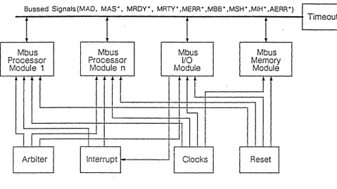
Rev 1.2 4/10/91using a subset of the MBus signals. namely a 64-bit multiplexed address/data bus (MAO(63:01)' an address strobe signal (MAS·). and an encoded acknowledge on three signals (MAOY'". MATY'". MEAA-). Additional level 1 signals support arbitration for modules (MBR· • MBG" • MBS") as well as interrupt inputs (IRl[3:0]). interrupt output (INTOUT"). reset (RSTIN·). asynchronous errors (AERR'"). scan (SCANOI • SCANoO. SCANClK. SCANTMS1. SCANTMS2) and module identification (10(3:0». The MBus reference clock (ClK) completes the signal requirements for a level 1 system.
It is assumed that there are central functional elements to perform reset. arbitration. interrupt distribution. time-out, and MBus clock generation as shown in Figure 1. All modules with the exception of processor and Timeout modules accept an 10(3:0] input which .is used as an aid to system configura-tion. Also the binary value input to a module on 10 [3: 0] is output as part of MAD (63 :0] during the address phase of every transaction.
Bussed Signals(MAD, MAS'". MROY'". MRTY- ,MERR" ,MBS'" ,MSH- ,MIH- ,AERR-)
Timeout
Mbus
Mbus
Mbus
Mbus
Processor
Processor
I/O
Memory
Module 1
Module n
Module
Module
r-"
'
-l
I,
I
Arbiter
Interrupt
Clocks
Reset
Figure 1 - MBus System Elements and their Connectivity.
1.2.2.
Level
2
Overview
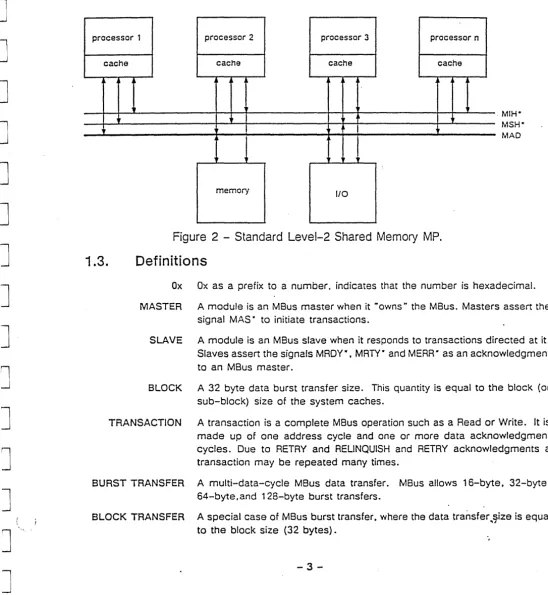
The Level 2 MSus includes all Level 1 transactions and signals and adds four transactions and two signals to support cache coherency. This is to facilitate the design of shared memory multi-processor systems. In level 1. details of the caches inside modules are not visible to the MBus transactions. This changes with level 2, where many aspects of the caches are assumed as part of the new MBus transac-tions. To participate in sharing between processor caches on an MBus using level 2 transactions, a cache must minimally support a "write back" policy. an "allocate" policy on write misses. and have a block or sub-block size of 32 bytes. Cache lines are assumed to have at least five states (invalid. exclusive clean. exclusive dirty. shared clean. and shared dirty).
The additional transactions present in Level 2 systems are Coherent Read. Cohere~t Invalidate. Coherent Read and Invalidate. and COherent Write and Invalidate. The two additional signals are Shared (MSH -) and Inhibit (MIH"). Coherent transactions. with one rare exception (Coherent Write and Invali-date used with write through caches) have SIZE
=
32 bytes. The cache coherency protocol is a "write,
-2-]
]
]
]
J
J
]
]
]
]
]
]
]
l
SPARC™ . MBus
. Interface Specification
Rev 1.2 4/10/91invalidate" protocol. where the cache being written issues a Coherent Invalidate transaction if the line is not exclusive. This indicates to all caches that they should immediately invalidate the line since it will contain "stale data" after the write completes. All caches "snoop" Coherent Read transactions and assert MSH· if the address of the transaction is present in their cache. By observing MSH· • caches can update the state of the lines they hold. If a cache is the "owner". it asserts the signal MIH· to tell memory not to send data and then supplies the data to the requesting cache. Coherent Read and Invalidate. and Coherent Write and Invalidate are simply the combination of a Coherent Invalidate with either a Coherent Read or a Write. Their purpose is to reduce the quantity of MBus transactions needed and thus conserve bandwidth. Figure 2 shows a simplified MBus MP system.
processor 1 processor 2 processor 3 processor n
cache cache cache cache
1.3.
I
memory 1/0
Figure 2 - Standard Level-2 Shared Memory MP.
Definitions
. MIH- MSH-MAD
Ox Ox as a prefix to a number. indicates that the number is hexadecimal.
MASTER A module is an MBus master when it "owns" the MBus. Masters assert the signal MAS" to initiate transactions.
SLAVE A module is an MBus slave when it responds to transactions directed at it. Slaves assert the signals MRDY· • MRTY" and MERR" as an acknowledgment to an MBus master.
BLOCK A 32 byte data burst transfer size. This quantity is equal to the block (or sub-block) size of the system caches.
TRANSACTION A transaction is a complete MBus operation such as a Read or Write. It is made up of one address cycle and one or more data acknowledgment cycles. Due to RETRY and RELINQUISH and RETRY acknowledgments a transaction may be repeated many times.
BURST TRANSFER A multi-data-cycle MBus data transfer. MBus allows 16-byte. 32-byte. 64-byte.and 128-byte burst transfers.
BLOCK TRANSFER A special case of MBus burst transfer. where the data transfer .. ~ize is equal to the block size (32 bytes).
-3-J
J
o
c
o
o
]
]
]
o
o
o
SPARC™. MBus
Interface Specification
Rev 1.2 4/10/91OWNED A block of data is said to be owned when there is one (and only one) cache in the system which is responsible for writing it back to memory as well as supplying the block when requested by other caches. If no cache is the own-er. memory is considered the ownown-er.
SHARED A block of data is said to be shared when more than one cache i~ the system currently possesses a valid copy of it.
EXCLUSIVE A block of data is said to be exclusive when there is only one cache in the system which contains a valid copy of it.
DIRTY A block of data is said to be dirty when it has been written to in a write-back cache. Dirty blocks must be written back to main memory if displaced (vic-timized). A dirty block is "OWNED" by that cache block.
VALID A block of data is said to be valid when it is present within a processor's cache and can be supplied to that processor upon request. Valid means the cache line is in one of four states: exclusive clean. exclusive dirty. shared clean. or shared dirty.
WRAPPING This concerns the order in which data will be delivered for multi-cycle trans-fers. For MBus. Read transfers larger than 8 bytes require multiple cycles. Wrapping implies that the data to be delivered first is specified by the low order address bits. i.e. the transfer address may not be burst size aligned.
1.3.1.
Compliance and Additional Features.
Full compliance with either Level 1 or Level 2 implies a certain minimal functionality within the MBus modules. particularly Level 2 modules where details of the module caches are exposed. Modules may contain more than this level of functionality either to enhance perform.ance. or to enable building a broader range of systems from MBus components. This is at the discretion of module designers and is implementation specific. An example of a performance enhancement is reflective memory support where memory is updated by observing the data being transferred from cache to cache. An example of functionality enhancement is support for simple second level caches. It is not within the scope of the MBus specification to cover details of these enhancements. MBus is merely a defined set of transactions operating on a defined set of signals. Module enhancements will be covered as .. application notes" by module designers and vendors. See appendix B for some insight into the nature of the two enhance-ments mentioned above.
1.4.
Basic Assumptions for Level 2
• Consistency Quantity
• Cache Write Policy
The data quantity upon which consistency will be maintained will be a cache block or. when implemented. a cache sub-block. It is also assumed that the same (sub-) block size will be used throughout the system and corresponds to the MBus Block size of 32 bytes.
While playing the Level 2 consistency game. all caches in the system will follow a write-back policy with write allocate.
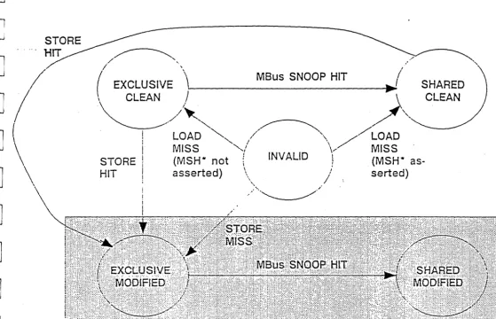
• Cache Consistency Protocol
An ownership-based protocol will be employed. A simplified state transition diagram is shown below in Figure 3.
4-o
o
o
o /
J/
0\
o \
]
]
J
C
SPARC™ MBus
Interface Specification
• Homogeneous Modules
Rev 1.2 4/10/91
All modules using the same MBus will play the same consistency game. The modules will appear identical as far as the MBus is concerned. yet they may differ internally .
• Second-Level Caches
It is assumed that all second-level caches will be physically addressed.
~,
./ '.
(
I \\
MBus SNOOP HIT
I
EXCLUSlVE
~
SHARED
,
CLEAN
J
/
CLEAN
. \
/l~
'"~,./
'",-~
. t
LOAD ""-,
//
'\ //LOAD
I " I \
I
MISS
'""/
\/
MISS
STORE
I
(MSH*
not
(
INVALID
J(MSH*
as-HIT
!
asserted)
\.
j
serted)
i
..
:>-.,'-___ -/,/
I
!
/
o
]
SOFTWARE FLUSH OR MBUS COHERENT OPERATIONS WITH INVALIDATE (CI, CWI, CRI)
CAUSE ANY STATE TO GO TO INVALID. FLUSH AND VICTIMIZATION WILL INVOLVE COPY-OUT
IF OWNED.
o
o
o
Figure 3 - Simplified cache block state diagram.
o
j
o
o
o
o
]
]
J
]
o
J
o
o
o
o
SPARC™ MBus
Interface Specification
Rev 1.2 4/10/91Chapter 2
'~. .... : ....
2.
Signal Definition
2.1.
Physical Signal Summary
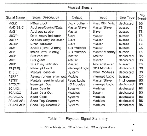
Table-1 summarizes al\ the MBus Module physical signals. An asterisk (") following the signal name indicates that the signal is active low (true when '0').
Physical Signals
Signal Name Signal Description Output Input Line Type Typet Sig
MCLK MBus clock clock buffer Mast./Slv.l Arb. dedicated BS
MAD[63:0] Address/Control/Data Master/Slave Master/Slave bussed TS
MAS" Address strobe Master Slave bussed TS
MROY" Data ready indicator Slave Master bussed TS
MRTY- Xaction retry indicator Slave Master bussed TS
MERR" Error indicator Slave Master bussed TS
MSH" Shared (level-2 only) Bus Watcher Master bussed 00
MIH" Inhibit (level-2 only) Bus Watcher Master/Memory bussed TS
MBR" Bus request Master Arbiter dedicated BS
MBG" Bus grant Arbiter Master dedicated BS
MBB- Bus busy indicator Master Arbiter/Master bussed °TS
IRL[3:01 Interrupt Level Interrupt Logic CPU Modules dedicated BS
10 [3:01 Module Identifier System MBus Modules dedicated BS
AERR" Asynchronous error out Module Interrupt Logic bussed 00
ASTIN" Module reset in signal Reset Logic Master/Slave impl depen BS
INTOUT- Interrupt Out 110 Modules Interrupt Logic dedicated BS
SCANOI Scan Data In System Modules dedicated BS
SCANDO Scan Data Out Modules System dedicated BS
SCANCLK Scan Clock System Modules dedicated BS
SCANTMS1 Scan Tap Control 1 System Modules dedicated BS
SCANTMS2 Scan Tap Control 2 System Modules dedicated BS
Table 1 - Physical Signal Summary
...
,
t BS
=
bi-state. TS=
tri-state 00=
open drain-6-I .J
]
]
]
o
o
]
l
.J
J
]
o
o
o
o
SPARC™ MBus
Interface Specification
Rev 1.2 4/10/912.2.
Physical
Signal Descriptions
MCLK MBus master clock. The distribution of the MCLK signal in a system is implemen-tation dependent. For example. depending on the connector, each module on the MBus may be given one or more identical MCLK lines which could originate from a single clock generator.
MAD[63:0] Memory Address and Data. During the address phase, MAD[35:01 c'ontains the physical address (PA[35:0J). The remaining signals (MAD(63:36]) on the bus contain the transaction-specific information which will be described in section 2.4. During the data phase, MAD[63:0] contains the data of. the transfer. The bytes are organized as shown in Figure 4. For transactions involving less than a double word (8-bytes), the data must be aligned. For example. all even-ad-dressed words will be aligned on MAD(63:32] whereas all odd-adeven-ad-dressed words will be aligned on MAO[31 :0]. As another example, byte address 2 of an odd-addressed word will be carried on MAD [15:8] i.e. byte 6 on the MBus. Unused data lines during the data phase are undefined.
MAD. 63 56 55 48 47 40 39 32 31 24 23 16 15 8 7
o
,
,
~
-
--;-..
-
---!--
-
--;-..
-
~,
,
,
'15
I halfword 0 0 15 halfword 1 0115 I halfword 2 0
15 halfword 3 01
31 word 0 o 31 word 1 o
Figure 4 - Byte Organization
MAS" Memory Address Strobe. This signal is asserted by the bus master during the very first cycle of a bus transaction. The cycle in which it is asserted is referred to as the "address cycle" or "address phase" of the transaction. For transac-tions that receive a Relinquish and Retry or a Retry acknowledgment, .MAS· will be asserted again until the transaction gets a normal or error acknowledgment. Other cycle timing is discussed with respect to MAS". e.g. A+2 indicates the second cycle after MAS" assertion. i. e. MAS" assertion is A+O.
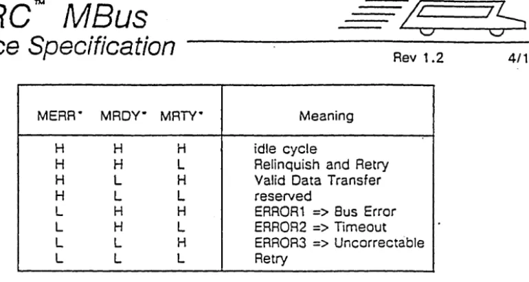
MRDY" MBus ready transaction status bit. This bit is one of the three bits used to en-code the transaction status as shown in Table 2. The encoding with MRDY" asserted alone indicates that valid data has been transferred. The three status bits (MRDY·. MRTY", and MERR") are normally asserted by the addressed slave. The ERROR2 (Timeout) acknowledgement will be asserted by the bus monitor.
",
-7-~ .. ~.-• • - - _ \ . . . -~.-- . , . . . . # • • • • • • _ • • • • •
]
]
o
o
o
J
o
o
J
J
o
o
o
J
o
o
o
o
SPARC™ MBus
Interface Specification
MEAR· MROY· MRTY·
H H H
H H L
H L
H
H L L
L H H
L
H
LL L H
L L L
Rev 1.2
Meaning
idle cycle
Relinquish and Retry Valid Data Transfer reserved
ERROR1 => Bus Error ERROR2 => Timeout ERROR3 => Uncorrectable Retry
Table 2 - Transaction Status Bit Encoding
4/10/91
MRTY* MBus retry transaction status bit. This bit is one of the three bits used to encode the transaction status as shown in Table 2. The encoding with MATY" asserted alone indicates that the slave wants the master to abort the current transaction immediately and start over. The master will relinquish bus ownership upon this type of a retry acknowledgment; Note that if any type of acknowledgement other than "Valid Data Transfer" is issued, the cycle it is issued is the last cycle, regardless of how many further acknowledgement cycles would normally occur. The three status bits (MRDY", MRTY- , and MERR-) are normally asserted by the addressed slave.
MERR· MBus error transaction status bit. This bit is one of the three bits used to encode the transaction status as shown in Table 2. The encoding with MERR" asserted alone indicates that a bus error (or other system implementation specific error) has occurred. Note that if any type of acknowledgement other than "Valid Data Transfer" is issued, the cycle it is issued is the last cycle, regardless of how many further acknowledgement cycles would normally occur. The three status bits (MRDY·, MRTY", and MERR·) are normally asserted by the addressed slave.
MBR * MBus Request signal. This signal is asserted by an MBus master to acquire bus ownership. There is one unique MBR- signal per master.
MBG· MBus Grant signal. This signal is asserted by the external arbiter when the par-ticular MBus master is granted the bus. There is one unique MBG" signal per master.
MBS· MBus busy signal. This signal is asserted as an output during the entire transac-tion, from and including the assertion of MAS" to the assertion of the last MRDY· or first other acknowledgment which terminates the transaction (such ~s an er-ror acknowledgment). If a master wishes to keep the bus and perform several transactions without releasing the bus between them, it keeps MBB" asserted until the last MRDY - of the last transaction of the group. The potential master device samples this signal in order to obtain the bus ownership as soon as the current master releases the bus. MBB" locks arbitration on a particular MBus. A master is allowed to assert MBB - prior to the assertion of MAS -.. ,(to hold the bus) . It is also allowed to keep MBS· asserted after the assert.ion of the last
-8-l
.J
o
o
o
o
o
o
J
o
o
o
o
o
o
o
o
SPARC™ MBus
Interface Specification
Aev 1.2 4/10/91acknowledgment in a few special cases for performance reasons. This contin-ued assertion of MBB" should only occur while MBG" is still parked on the current master. The MAS· of the transaction prompting the continued assertion of MB8" should be generated quickly (2 cycles is the recommended maximum delay). For more details on arbitration see section 4.2.
MIH- Memory InHibit signal. This signal is only present in level-2 MBus modules. It is asserted by the owner of a cache block at the beginning of the second cycle after it receives the address (its A+2 cycle) t to inform the Main Memory that the current Coherent Read or Coherent Read and Invalidate request should be ig-nored. This is because the owner. not the Memory. will be responsible for deliv-ering the cache data block. If no device asserts MIH" during its A+2 cyclet. main memory will be responsible for delivering the data. If main memory starts deliv-ering data and MIH" is asserted. the memory delivery shall be aborted immedi-ately. Any data which was received from main memory in this case should be ignored. It should be noted that because of the restriction on MIH" either occur-ring simultaneously with or before MRDY" , there will be at most two cycles worth of data to ignore. While MIH" is sourced by a module (for one cycle) two cyclest after receiving MAS" it may be observed by a cache in the inter:val from' its A+2 until it observes an acknowledgement. This variation in wher§ MIH" can be ob-served is due to the possibility for MBus repeaters and mOdules that do not meet the A+2 timing.
MSH - Cache block SHared signal (wired-or. open-drain). This signal is only present in level-2 MBus modules. Whenever a Coherent Aead transaction appears on the bus. the bus monitor of each processor module should immediately search its cache directory. If a valid copy is found. the MSH" signal should be asserted in the second cycle after the address is received (its A+2 cycle)
t.
The MSH" signal is also sampled (observed) by external caches. It is c:sserted as an output (for a single cycle) if there is a cache hit in the snooping directo·ry. While MSH" is sourced by a module two cycles t after receiving MAS" it may be observed by a cache from its A+2 until it observes an acknowledgement t . This variation in where MSH" may be observed is due to the possibility for MBus repeaters and modules that do not meet the A+2 timing. Signals are sourced at the beginning and observed or sampled at the end of a cycle. Due to the open drain nature of MSH" and the associated slow rise time. while the signal is driven active low for one cycle. it can be observed active low for up to two cycles and the trailing or rising edge of the signal is considered asynchronous.RSTIN" Module reset input signal. This signal should reset all logic on a module to its initial state. and ensure that all MBus signals are inactive or tri-state as appropri-ate. The minimum assertion time of RSTIN" will be system implementation de-pendent. although the default assertion time will be 1 024 MBus clock (MCLK) periods(2S.6 microseconds). ASTIN- should be treated as asynchronous.
AERR· Module asynchronous error detect out signal. This signal is asserted by the ule as a level to indicate that an asynchronous error was detected by the mod-ule. It remains asserted until a software initiated action resets a bit that is main-taining the signal assertion. AERR" is open drain because several modules could assert it simultaneously. AERR" may be asynchronous.
t
See Appendix 8.5. for notes to designers who wish to avoid the A+2 requiremen~.-o
o
o
c
c
o
o
o
o
o
o
o
o
o
o
o
o
o
o
SPARC™
MBus
Interface Specification
Rev 1.2 4/10/91INTOUT- Module Interrupt out signal. This signal is asserted by an ,110 module as a level to indicate an interrupt request to the system. It remains asserted until a software initiated action resets a bit that is maintaining the signal assertion. INTOUT- may be asynchronous. This signal is optional.
IRL[3:01 These pins carry the Interrupt Request level inputs to a SPARC Integer Unit. They are only used by processor modules. IRL[3:01 may be asynchronous. Each pro-cessor module receives a dedicated set of IRL[3:0].
10[3:01 These pins carry the Module Identifier. These signals are not needed by Levell processor modules, which have a default 10 of OxF, and are optional for other modules who may obtain this information by other means: 10[3:01 is reflected as MI0(3:0] during the address phase of every transaction. and is also used to identify a unique address range for Module identification, initialization and con-figuration.
If modules do not have 10(3:0] input pins. the system must provide a function that allows each module to obtain a unique 10(3:0} value in an internal 10[3:0] register. One way this can be accomplished is to have a logic function with a known MBus address attached to the MBus arbiter. There are unique MBR· and MBG - lines per module and so this function when addressed, would return a unique 10(3:01 value on MAD, based on whic::h module's MBG- was asserted just prior to the beginning of the 10 Read transaction when MBa - was de-asserted.
SCANOI This Signal corresponds to the signal TOI as described in IEEE Pl149.1 (here after referred to as Pl149) . It is an input to the module and is used for receiving scan data from the system. This is the input of the scan ring and should not be inverted or gated. This signal changes on the falling edge of SCANCLK and should be sampled on the rising edge of SCANCLK. Scan is optional.
SCAN DO This signal corresponds to the signal TOO as described in P1149. It is an output of the module and is used for sending the scan data to the system. This is the output of the scan ring and should not be inverted or gated. SCANDO should be driven on the falling edge of SCANCLK and will be sampled on the rising edge of SCANCLK. Scan is optional.
SCANCLK This signal is used to supply the clock to the scan ring on the module. (Typically 5 MHz) Scan is optional.
SCANTMS1 This signal is an input to the module. It is used to control the TAP controller state machine. It corresponds to the TMS signal as described in P1149. Scan is op-tional.
SCANTMS2 This signal is an input to the module. It is used to reset the TAP controller state machine. It corresponds to the TRST- signal as described in Pl149. Scan is optional.
2.3_
Multiplexed Signal Summary
Table 3 summarizes the multiplexed MBus signals. All multiplexed signals are actiye high (true when '1').
-n
U
o
c
c
n
L.J
o
J
J
o
c
D
c
o
o
o
o
SPARC™ ivlBus
Interface Specification
Rev 1.2 4/10/91Multiplexed Signals (valid during address phase)
Signal Name Physical Signal Signal Description
PA[35:0] MAD[35:0] Physical address for current transaction
TYPE[3:0] MAD[39:36] Transaction type
SIZE[2:0] MAD[42:40] Transaction data size
C MAD[431 Data cacheable (advisory)
LOCK MAD [44] Bus lock indicator (advisory)
MBL MAD[451 Boot mode 1 local bus (advisory) (optional)
VA[19:12] MAD[53:461 Virtual address (optional) (level-2)
reserved MAD[58:541 reserved for future expansion
SUP MAD[591 Supervisor Access Indicator(advisory) (optional)
MID[3:01 MAD[63:60] Module Identifier
Table 3 - Multiplexed Signal Summary
2.4.
Multiplexed Signal Descriptions
PA[35:0] Physical address of current transaction which is multiplexed on MAD[35:0].
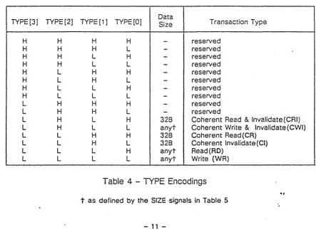
TYPE[3:0] The transaction types are encoded in bits MAD[39:36] as shown below in Table 4. Most of the transaction types are reserved.
TYPE [2] TYPE (1 ] TYPE [OJ Data Transaction Type
TYPE [3] Size
H H H H
-
reservedH H H L
-
reservedH H L H
-
reservedH H L L
-
reservedH L H H
-
reservedH L H L
-
reservedH L L H
-
reservedH L L L
-
reservedL H H H
-
reservedL H H L
-
reservedL H L H 32B Coherent Read & Invalidate (CRI)
L H L L anyt Coherent Write & Invalidate (CWI)
L L H H 328 Coherent Read(CA)
L L H L 328 Coherent Invalidate(CI}
L L L H anyt Read(RD)
L L L L anyt Write (WR)
Table 4 - TYPE Encodings
...
,
t
as defined by the SIZE signals in Table 5-]
]
J
C
o
o
J
'~
J
J
]
0
J
0
0
o
o
o
o
~-.----..
----.---. ----.---.----.---.
-SPARC™ MBus
Interface Specification
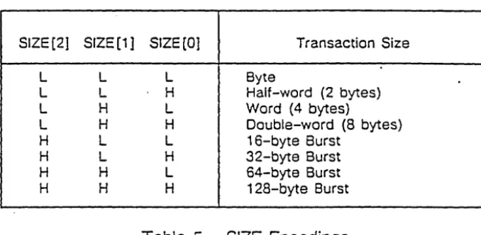
Rev 1.2 4/10/91SIZE[2:01 The transaction data SIZE information is encoded in bits MAD(42:401. The size field is encoded as logz (number of data bytes transferred1. The encoding of the SIZE bits is shown in Table 5.
SIZE[21 SIZE [1] SIZE(O] Transaction Size
L L L Byte
L L H Half-word (2 bytes)
L H L Word (4 bytes)
L H H Double-word (8 bytes)
H L L 1 6-byte Burst
H L H 32-byte Burst
H H L 64-byte Burst
H H H 128-byte Burst
Table 5 - SIZE Encodings
-'If
wetplN~Jf
For transactions with SIZE greater than 8 bytes, more than one MRDY" will be needed. For read transactions, MSus supports a feature called "wrapping". During the address phase, MAD[2:0} are don't care. and MAD(35:31 defines the 8 bytes to be returned with the first MRDY". This means that the address defines which data to return first, and this will vary. Data returned on subsequent MRDY"s will be for the address associated with incrementing MAD[n:3] where n=
3 for SIZE=
16-bytes, n=
4 for SIZE=
32-bytes, up to n=
6 for SIZE=
128-by-tes. As the address is (conceptually) incremented, the MAD[n:3] field will wrap around without incrementing MAD [3S:n+1], which is static for the duration of transaction.Wrapping affects all modules that have to deliver data with SIZE greater than 8 bytes. An exception is Level 2 cache controllers, which'may choose not to support wrapping for snoop read hits, when they supply the data. This means that Level 2 processor modules that don't support wrapping on the snoop port cannot share an MBus with Level 2 MBus processors that issue "wrapped" re-quests. To ensure maximum compatibility, Memory and 110 modules should all support wrapped requests to their slave ports. but should only issue aligned requests from their master ports.
The wrapping feature is not supported for writes. Write transactions with Size greater than 8 bytes should have address bits MAD [n:3] be zero, and MAD (2:01
are undefined as for reads.
For transactions with SIZE less than or equal to 8 bytes, unneeded address lines are undefined. e.g. for SIZE = 8 bytes, MAD[2:0] are undefined.
VA[19:12] Virtual Address 19 through 12 (multiplexed on MAD[53:46}). This field only ap-plies to MBus level-2 Coherent transactions. It is used to carry the virtual ad-dress bits 19 through 12 associated with the physical adad-dress of a Coherent Read transaction. These bits are used by virtually indexed caches that desire to index into the dual directories via the virtual "superset" bits to avoid synonym problems. This assumes a minimum page size of 4K in the syst~m and
12-o
o
c
o
o
o
o
J
o
o
o
o
o
o
o
o
o
SPARC
NMBus
Interface Specification
Rev 1.2/~----s
4/10/91mum cache size of 1 MS. Modules that choose not to provide this function nor to support non-coherent transactions (such as a level-1 device) should drive these lines high.
MID[3:0] Module identifier signals (multiplexed on MAO(63:60J). This field is sourced by all MBus modules and reflects the value input into the module on the 10 [3 :0] input signals. For level-1 processor modules this field is driven high(OxF) .. This field is observed by slave ports that wish to issue a Relinquish and Retry acknowl-edgment(see section 3.4). so that they can identify the master with which to re-connect in a mUlti-master system configuration.
C Cache able indicator (multiplexed on MAD[43]). When this signal is asserted. it indicates the state of the cacheable bit for the address of the transaction in the module MMU (if there is one). If a module has insufficient information to deter-mine the level of this bit for a transaction. it should leave the bit de-asserted. This is an advisory bit. not used by MBus transactions. but possibly of use to the slave device.
LOCK
An example use of C would be to inform a second level cache of the cacheability state of the address of a transaction with SIZE less than 32 bytes.
lock indicator signal (multiplexed on MAD [44]). If the MBus master intends to lock access to a device residing on MBus (main memory is one MBus device) or some other bus connected to MBus. and perform N indivisible MBus transactions to the device. this bit needs to be asserted during the address cycles of all N
MBus transactions. The locking master must keep MBB" asserted during each locked cycle and not de-assert it until the end of the final locked transaction (however MBB· may be suspended for a time by an R&R acknowledgment). The de-assertion of MBB" signals the MBus arbiter to release the MBus. It is the final de-assertion of MBB" after possible intervening R&R acknowledgments which tells the device to release its lock. lOCK is an advisory bit. not used by MBus transactions directly. but possibly of use to the slave device or bus interface.
An example use of LOCK would be to "lock" an MBus master to a particular slave. If an MBus processor pertormed an atomic operation to a resource arbi-trated externally to MBus. such as a dual-ported memory device or an9ther bus. then the external arbiter could prevent any other (non MBus) device from ac-cessing that resource by locking arbitration. The referenced slave device in a LOCKed transaction could be. in essence. dedicated to the requesting master. The MBus slave port interface interprets an assertion of the MBus LOCK bit as saying .• become locked" and a final de-assertion of MBB· at the end of the locked sequence as saying" become unlocked" • and reports this information to the arbiter for the "locked" device (or bus). If the slave port supports R&R ac-knowledgments. it must know not to clear the locked state when MBB" is re-moved due to an R&R.
MBl M8us boot mode / local bus indicator (multiplexed on MAD (45]). This signal is asserted by processor modules during the address phase of boot mode transac-tions. or during local bus transactions (SPARC processor accesses with ASI
=
Ox1) . It is system implementation dependent whether or not local bus transac-tions are employed in a system. This is an advisory bit. not used by MBus trans-actions. but possibly of use to the slave device. This bit is optionakslf unused by an implementation it should remain de-asserted.-l
-.J
c
r
L
n
u
o
o
o
o
o
o
o
o
o
o
o
o
o
SPARC™ MBus
Interface Specification
Rev 1.2 4/10/91SUP Supervisor access indicator (multiplexed on MAD [59]) . This signal is asserted by processor modules and indicates that the M8us transaction is a processor Supervisor access. This is an advisory bit. not used 'by MBus transactions. but possibly of use to the slave device. This bit is optional. If unused by an imple-mentation it should remain asserted.
An example use of SUP would be to enable more state to be captured on proces-sor asynchronous write errors.
reserved This 5-bit field (multiplexed on MAD [58:54]) • is reserved for future MBus expan-sion. The lines should be driven high if not used.
-"I
.-J
~l
--.J
n
L.
C
I l
'--...J
C
0
C
0
C
0
0
c
0
c
0
0
0
0
• ... ___ • o.
SPARC™ MBus
Interface Specification
".;.'
3.
MBus Transactions
3.1.
Semantics
Rev 1.2 4/10/91
Chapter
3
(1) Basic cycle is read/write(size) , where size is from 1 to 128 bytes.
(2) Bus cycles greater than 8 bytes are performed as bursts.
(3) Data rate is controlled by the slave. Master must be able to accept a burst read, or source a burst write. of requested size, at maximum transfer rate.
(4) Master starts bus cycle with MAS· (address transfer phase). Master also asserts MBB· at (or before) this time.
(5) In the case of burst mode, multiple acknowledgments are used and the bus cycle ends with the acknowledgment of the last data transfer. The master de-asserts MBB· at end of the last cycle (except for locked bus cycles).
(6) Locked bus cycles are an indivisible sequence of basic bus cycles. Locked cycles are also terminated immediately by error acknowledge and individual transactions in the sequence may be suspended by retry or relinquish and retry acknowledgments.
Note: In the transaction semantic diagrams that follow, optional wait states are indicated as x, y. or z cycles. x, y, and z can be zero.
3.2.
Level 1 Transaction Types
3.2.1.
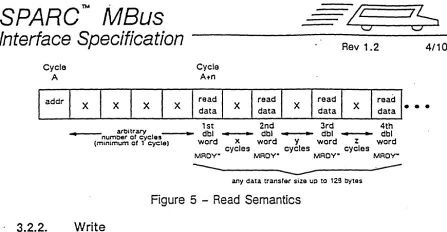
Read
A Read operation can be performed on any size of data transfer which is specified by the SIZE bits in Table 5. Read transactions support wrapping as defined in section 2.4. Read transactions involv-ing less than 8 bytes will have undefined driven data on the unused bytes. The minimum MBus Read transaction will take 2 cycles. This minimum time is for the cases when no data is returned on MAD, such as during R&R or error acknowledgements. If data is being returned. an extra cycle is required to avoid bus contention. The arbitration protocol creates a dead cycle between transactions which ensures there will be no bus contention between back-to-back reads from different masters. If a module locks the bus and performs back-to-back reads. it is its responsibility to ensure a dead cycle to avoid contention Note that the protocol means that a master
must
be able to receive data at the maximum rate of the MBus for the duration of the transaction. i.e. 8 bytes on every consecutive clock. Figure 5 depicts the semantics of a Read operation. Refer to Chapter 8 for details pertaining to cycle waveforms...
,
-l
--l
]
c
D
o
D
D
D
o
o
D
o
D
o
o
SPARC™
MBus
Interface Specification
Rev 1.2Cycle A
addr
3.2.2.
X
•
X X X
Cycle
A ... n
read data X
read read read data X data X data , st 2nd 3rd 4th
arbitrary - - 4 . . . dbl ...-- dbl • • dbl . . . - - - dbl
number of cycles
(minimum of 1 cycle) word x word Y word Z word cycles cycles cycles
MADV· MADV· MADV·
MADY-any data transfer size up to 129 bytes
Figure 5 - Read Semantics
Write
4/10/91
• • •
A Write operation can be performed on any size of data transfer which is specified by the SIZE bits in Table 5. Write transactions involving less than 8 bytes will have undefined data on the unused bytes. The writing master will immediately drive the data in the period after the address phase of the transaction, and immediately after receipt of each MRDY" in transactions with SIZE greater than 8 bytes. Note that the protocol means that a master
must
be able to source data at the maximum rate of the MBus for the duration of the transaction, i.e. 8 bytes on every consecutive clock. The minimum MBus Write operation will take 2 cycles (minimum is actually 3 cycles if different masters are performing back-to-back writes). Figure 6 shows the basic semantics of a Write operation.Cycle
A
addr
.
.
I I I
,
I ICycle
A+n
I write
,
,
I write I,
write I,
write data 1 ,data 1 I data 1.
I data 1 , data 1 data 2 , cata 2 data 3 I data 3 cata 4 I data 4OIl
1 st 2nd 3rd 4th
arbitrary
--1."
dbl ~ dbl ....--- dbl - - dblnumber of cycles word x word Y word Z word cycles cycles cycles
MADY· MADV· MADY· MADY·
any data transfer size up to 128 bytes
Figure 6 - Write Semantics
•
•
•
Due to the nature of the cache-consistency protocol, the Write transaction works equally well in level 1 and Level 2 MBus implementations. Writes can be used for non-cacheable accesses as well as for write-backs of dirty (sub-}blocks. Write transactions do not need to be sn,?oped and the MIH" and MSH" signals must not be asserted during the operation. .
R&A acknowledgements issued to Block Write transactions to cacheable locations introduce a detailed design problem. in that the write back buffer in this case may be the only source of the most up to date data. This introduces the prospect of having to snoop the write back buffer. To simplify the design of processor modules. the MBus specification eliminates the need for processor modules to snoop write back buffers and places the burden of handling this case of R&R acknowledgement on the module that issues the R&R. Modules that issue R&R acknowledgements to cacheable block write transactions must capture the address (es) of the cache line (s) until they complete the transaction to which they issued R&A. Should other modules attempt to read the line(s) during this interval the R&A issuing module must detect this and issue R&R to the intervening Coherent Read (CR) or Coherent Read and InVjllidate (CRI) transaction(s). In general it should be possible for most modules to avoid the need to .,issue R&A to
-
o
o
o
o
o
o
o
o
o
o
o
o
o
o
o
o
SPARC™
MBus
Interface Specification
Rev 1.2 4/10/91cacheable block write operations and hence avoid this complexity. The only likely exception is a coherent bus adaptor.
3.3.
Additional Transaction Types for Level 2
3.3.1.
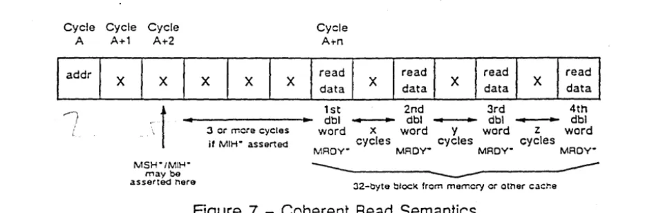
Coherent Read
A Coherent Read operation is a block read transaction that maintains cac~e consistency. The participants in the trarisaction are the requesting cache, the other caches which snoop, and memory (or a second level cache). There are three possible read scenarios which the caches that snoop can experi-ence:
a)
b)
c)
For a snooping cache which does not have a copy of the requested block. it simply ignores this transaction.
For a snooping cache which does have a copy of the requested block but does not own
it. it simply asserts MSH - for one cycle during its cycle A+2t. It will mark its copy as shared (if not already marked as such).
For a snooping cache which owns the requested block. it will assert both the MSH· and MIH - signals for one cycle during bus cycle A+27 and start shipping the requested data no sooner than its cycle A+6, (4 cycles after it issued MIH-). If its own copy of the block was labeled exclusive. it will be changed to shared. f;3lse no status change will take place for its own copy.
Upon receiving the data block. the requesting master shall label the block exclusive if no one . asserts MSH· during its cycle A+2t and shared if the signal MSH - is ~sserted during its cycle A+2t.
Figure 7 depicts the semantics of a Coherent Read operation where. memory latency is long.
Case (c) above needs further elaboration. This is the only case where MIH- is asserted. This signal affects three parties. It is sourced by the snooping (intervening) cache and observed by both memory (or a second level cache) and the requesting cache. It tells the requesting cache that it may have received stale data from memory, and to ignore that data and data it may receive on the next clock and wait until the fourth or later clock for the correct data. It tells memory to stop sending data
immedi-ately, which means memory may send one more MROY- before it can stop. The delay of 4 clocks at the requesting cache and the snooping (intervening) cache serve two related purposes. The firsris to allow time for MRDY· and MAD from the memory to be turned off before the snooping cache asserts MRDY· and MAD. and so avoid bus contention. The second is to allow for implementations that buffer the MBus.
Cycle Cycle Cycle A A+l A+2
addr
X X X X X
Cycle A+n read data
read X
data
read read X
data X data 1 st 2nd 3rd 4th
I
... t__---...
dbl - - dbl.. • dbl.. • dbl,
MSH-'MIW
may be
asserted here
:3 or more cycles
jf MIH- asserted
word x word Y word Z word
cycles cycles cycles
MRDY- MRDY· MADY-
MRDY-32-byte blocK from memory or Other cache
Figure 7 - Coherent Read Semantics
t
See Appendix B.S. for notes to designers who wish to avoid the A+2 requiremen~.-c
o
o
c
[
o
o
o
o
o
o
o
o
o
o
o
o
o
o
SPARC™ MBus
Interface Specification
Rev 1.2 4/10/91The earliest that memory (or a second level cache) is allowed to issue MROY· (or any acknowl-edgment) is its cycle A+2t. This ensures that acknowledgments never occur before MIH·. Figure 7 shows the semantics of a Coherent Read transaction.
3.3.2.
Coherent Invalidate
An Invalidate operation can only be performed on a block basis. All Invalidate operations will be snooped. If an Invalidate operation hits in a cache, then that copy will be invalidated immediately. re-gardless of its state. One module ( normally a Memory controller) is responsible for the acknowledg-ment of the Coherent Invalidate transaction. This is accomplished on its cycle A+2t. or later. All acknowledgment types are possible. Memory will only ever issue normal acknowledgments(MROY-) to Coherent Invalidates, but coherent bus adaptors may issue other acknowledgments, particularly R&R. It should also be noted that a Coherent Invalidate transaction will have SIZE
=
328 during the address phase. but it will only be expecting one MROY· for the acknowledgment. Also the address may not be 32-byte aligned. Memory (or coherent bus adaptor) designers should take note of this. If in a particular system. caches cannot guarantee to complete their invalidation before their A+2t cycle, the memory controller for that system should delay the acknowledgment as appropriate. This implies that memory controllers should have a feature that allows the time to acknowledge invalidates to be varied to some extent, either hard wired or through a programmable register. A recommended range for the program-mable delay is A+2 to A+1 O. This programmable delay is the MBus flow control technique to guarantee that invalidates can be completed at any rate they are issued.This Coherent Invalidate M8us transaction is issued when a write is being performed into a cache line that is Shared. Before the write can actually be performed, all the other systems caches must have their local copies invalidated (write-invalidate cache-consistency protocol). Snooping caches will not assert MSH· during A+27. The MAD lines will contain undefined data during the data phase cycles. If
a
Coherent Invalidate transaction should receive an R&R acknowledgement there is a possibility that the line which is about to be written becomes invalidated by an intervening invalidation transaction on the bus. This means that when the cache regains the bus it should issue a Coherent Read and Invalidate transaction, not a Coherent Invalidate transaction, to once again allocate the (sub-)~Iock. Figure 8 shows the basic semantics of an Invalidate operation.
For any particular system, selecting which module will be responsible for acknowledging Co-herent invalidates introduces some issues for memory controller deSigners. In most systems a single memory controller will be responsible. In systems with a coherent bus adaptor, the adaptor will be re-sponsible. If it is desired to use a memory controller in a system that also has a coherent bus adaptor, it is then required to be able to tell the memory controller not to respond to invalidates. This should be accomplished during system initialization prior to enabling any caches, preferably by writing a bit in
a
register in a memory controller.
Cycle Cycle Cycle A A+ 1 A+2 or later
MRDY· or other ac\<
Figure 8 - Coherent Invalidate Semantics
t See Appendix B.S. for notes to designers who wish to avoid the A+2 requirement:'
,
18
---_.-._-_ .. _----_. __ .-'--", .. " .
]
c
c
o
n
o
o
o
o
o
n
LJ
o
o
o
o
o
SPARC™ MBus
Interface Specification
3.3.3.
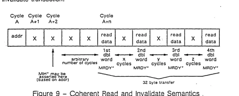
Coherent Read and Invalidate
Rev 1.2 4/10/91
Since the MBus supports a write-invalidate type of cache-consistency protocol. a special Co-herent Read and Invalidate transaction. which combines a CoCo-herent Read transaction with a CoCo-herent Invalidate transaction. was included to reduce the n,umber of MBus transactions. Caches that are per-forming Coherent Reads with the knowledge that they intend to immediately modify the data can issue this transaction.
Each Coherent Read and Invalidate transaction will be snooped by all system caches. If the address hits and the cache does not own the block. then that cache will immediately invalidate its copy of this block. no matter what state the data was in. If the address hits and the cache owns the block. then it will assert MIH- and supply the data. When the data has been successfully supplied. the cache will then invalidate its copy of this block. Figure 9 shows the basic semantics of a Coherent Read and Invalidate operation. Note that it is identical to the Coherent Read operation. except that the system caches will invalidate the block. All of the detailed comments concerning MIH· for the Coherent Read transaction apply equally to the Coherent Read and Invalidate transaction. MSH· is not driven during the Coherent Read and Invalidate transaction.
Cycle Cycle Cycle
A A .. 1 A;-2
addr
X X
t
X X
Cycle
A+n
read data
read X
data
read read X.
data X data 1 st 2nd 3rd 4th
.. ., dbl ...-- dbl - - - - dbl ... 1 - - - dbl
ar':litrary word x word y word Z word
numt::er at cycles cycles cycles cycles
MRDY- MRDY- MRDY-
MRDY-32 byte transfer
Figure 9 - Coherent Read and Invalidate Semantics,
3.3.4.
Coherent Write and Invalidate
A Coherent Write and Invalidate transaction combines a Write transaction with a Coherent Invali-date transaction. The Coherent Write and InvaliInvali-date transaction is intended to reduce the n'umber of MBus transactions. This transaction can be used by Level-2 modules that wish to support a write through cache. a degree of functionality beyond the requirements for level-2 MBus. (Supporting write through caches is useful for implementing simple 2nd level caches that support inclusion.) CWI is also of use to block copy and block fill mechanisms.
Each Coherent Write and Invalidate transaction will be snooped by all system caches. If the address hits. then caches will invalidate their copies of this block no matter what state the data was in. Figure 10 shows the basic semantics of a Coherent Write and Invalidate operation. Note that it is identi-cal to the Write operation. except that the system caches will invalidate the block. All SIZE values are allowed and a single 32-byte block is invalidated regardless of the value of SIZE. Due to the nature of the cache coherency protocol neither MIH· nor MSH· are asserted.
All SIZE values are allowed in order to better accommodate write through caches. Systems with only either write through or write back caches work naturally. but a system with both a write through and a write back cache are very unlikely to work in a way that preserves cache consistency. This mixed system is not anticipated or recommended as a real MBus configuration.
-c
o
c
u
o
o
o
o
o
n
u
o
o
o
o
o
o
SPARC™ MBus
Interface Specification
Cycle Cycle
A A+n
addr I I I I I
,
, write,
data 1 I data 1 I data 1 , data 1 I data 11st
..
aroltrary..
dblnumber of cycles
word
MAOV·
---Rev 1.2
.
' write ' write '. write
,
,
,
data 2 I data 2 data 3 I data 3 data 4 , data 4
2nd 3rd 4th
...-...
dbl...
..
dbl..
..
dblx
word Y wordz
word cycles cycles cyclesMAOV" MAOV· MADV·
---
.---32 byte transfer
Figure 10 - Coherent Write and Invalidate Semantics
3.4.
Acknowledgment Cycles
4/10/91
It is a requirement that any transaction once issued must correctly accept any acknowledgment type. This applies to all Level 1 and Level 2 transactions. The earliest that an acknowledgment can be issued is A+1 for Read and Write and A+2 for all Coherent Transactions. Processor caches that are supplying data as part of a Coherent Read transaction may only issue either normal or error acknowl-edgements. They may not issue R&R or Retry acknowlacknowl-edgements.
3.4.1.
Idle Cycles
When there is no bus aCtivity or when it is necessary to insert wait states in between the address cycle and the data cycle or between consecutive data cycles. an addressed slave can simply refrain from asserting any transaction status bits (MERR". MRDY·. and MRTY"). The number of wait cycles which can be inserted is arbitrary, as long as it does not exceed the system timeout interval (see section
3~4,5. for timeout details).
3.4.2.
Relinquish
and Retry(R&R)
'wVhen a slave device cannot accept or supply data immediately. it can perform a relinquish and retry acknowledgment cycle by asserting MRTY" for only one bus cycle. This will indicate to the request-. ing master that it should release the bus immediately so that the bus can be re-arbitrated and possibly
used by another MBus master. This involves at least one dead cycle until the suspended transaction can be performed in the case when the bus is still granted to the re-trying master. When the bus is'no longer granted to the master in question. then the suspended transaction must wait until bus ownership is once again attained. When a transaction that receives an R&R acknowledgment regains bus mastership it must issue the same transaction over from the beginning. An exception to this is when a Coherent Invalidate turns into a Coherent Read and Invalidate (see section 3.3.2.). For Level 1 modules. for all transactions with SIZE greater than 8 bytes, a relinquish and retry acknowledgment can be asserted on any data transfer. For Level 2 modules, for all transactions with SIZE greater than 8 bytes, ( including the Level-1 READ and WRITE transactions) R&R can only be issued on the first acknowledgement. It is the responsibility of the slave port to time the duration of the transaction that is causing it to issue R&R. and return an ERROA2 acknowledgment to the correct master when its device specific timeout interval
(200 micro-s~conds is recommended) has passed and the master has re-connected to the slave.
There are two different cases that cause slaves to issue A&A