Spintronics based Random Access
Memory: A Review
Sabpreet Bhatti
1, Rachid Sbiaa
2, Atsufumi Hirohata
3, Hideo Ohno
4,
Shunshuke Fukami
4, and S.N. Piramanayagam
11. Division of Physics and Applied Physics, School of Physical and Mathematical
Sciences, Nanyang Technological University, Singapore.
2. Department of Physics, Sultan Qaboos University, P. O. Box 36, PC 123, Muscat,
Oman.
3. Department of Electronic Engineering, University of York, England.
4. Center for Spintronics Integrated Systems, Tohoku University, Japan.
Abstract
This article reviews spintronics based memories, in particular, magnetic random access
memory (MRAM) in a systematic manner. Debuted as a humble 4 Mb product by
FreeScale in 2006, the MRAM has grown to a 256 Mb product of Everspin in 2016.
Although this growth is not significant, MRAM has overcome several hurdles and have
reached a stage, where the potential for MRAM is very promising. One of the main
hurdles that the MRAM overcome between 2006 and 2016 is the way the information is
written. The 4 Mb MRAM used a magnetic field based switching technology that would
be almost impossible to scale below 100 nm. The 256 Mb MRAM, on the other hand uses
a different writing mechanism based on spin torque transfer (STT), which is scalable to
very low dimensions.
The paper starts with a brief history of memory technologies, followed by a brief
description of the working principles of MRAM for novice. Reading information from
MRAM, the technologies, materials and the physics behind reading of bits in MRAM are
described in detail. As a next step, the physics and technologies involved in writing
information are described. The magnetic field based writing and its limitations are
described first, followed by an explanation of STT mechanism. The materials and physics
behind storage of information is described next. MRAMs with in-plane magnetization,
their layered material structure and the disadvantages are described first, followed by the
advantages of MRAMs with perpendicular magnetization, their advantages etc. The
technologies to improve writability and potential challenges and reliability issues are
beyond the conventional MRAM technology are discussed at the end of the paper,
followed by a summary and an outlook.
Table of Contents
Abstract...2
1. Introduction...4
2. History...6
3. Working Principle of MRAM...8
4. Reading in MRAM : Magnetoresistance...13
5. Writing Methods for MRAM...19
6. Storage methods and choice of materials...25
6. 1. In-plane MRAM...25
6. 2. Perpendicular MRAM...27
6. 3. Thermal Stability...29
7. Writing improvements...32
8. Reliability issues of MRAM...36
9. Emerging Memories...38
9.1. New Writing Schemes...38
9.1.1. Spin Hall Effect based Memory...38
9.1 2. Electric Field Assisted Switching for MRAM...41
9. 2. Storage Schemes...44
9.2.2. Domain Wall memory...46
9.2.3. Skyrmion based memories...49
10. Summary and Outlook...53
1. Introduction
We live in the era of information and social networks. Due to the advent of high
performance computing and mobile devices with video cameras, enormous information is
generated and stored. This is made possible due to the growth in the storage and memory
technologies. Hard disk drives (HDD) with a capacity of 10 MB were sold for about
$5300 in the 1980s, and were unaffordable for many during Apple and IBM PC era.
However, HDDs with 12 TB capacity (a million times larger capacity) are available at the
time of writing (2017). The computers of the 1980s had memory of hundreds of kB. The
growth in the memory is also close to a million-fold and most common computers have
about 8 GB random access memory (RAM). Even mobile gadgets have a Dynamic
Random Access Memory (DRAM) capacity of about 4 GB, at the time of writing.
Despite such a growth, dynamic RAMs (DRAMs) which are based on semiconductor
technologies face limitations in maintaining a significant growth rate. The charge leakage
that occurs when the device sizes are scaled down causes an increase in power
consumption. A non-volatile memory would not consume much static power, in contrast
with dynamic RAMs. Due to potentially lower power consumption and instant-on
capability, a search for non-volatile memory technologies has been actively pursued for
more than a decade. Magnetic Random Access Memories (MRAM), which work on the
principles of spintronics, are intensively being researched at this point as a replacement
for several of the purely semiconductor based memory technologies. Spintronics based
magnetic random access memories such as Spin Torque Transfer MRAM (STT-MRAM)
Electrons have a charge and spin associated with them. While the conventional
semiconductor electronics makes use of the charge property of the electron only, the
spintronics devices makes use of the spin property of an electron. The use of magnetic
materials in spintronics devices help to store information, to provide non-volatility and to
provide an endurance that is unmatched by other memory technologies such as resistive
or phase-change memory. Making use of the spin nature of electrons provide new and
effective ways to control the motion of electrons, which help in writing and reading
information. More importantly, these mechanisms can be integrated on top of the
conventional Si-based memory technologies. As a result, these memory devices have a
huge potential. The aim of this review article is to introduce various types of current and
emerging spintronics-based memory technologies. The unique nature of the review article
lies in its tutorial format, explaining the basics and covering the breadth of this field to a
non-expert in this field.
In section 2, a brief history of memory devices and their evolution is presented. Section 3
gives a description of the working principles of MRAM. The basics behind the three
criteria required of a memory device, readability, writability and retention of data, are
described briefly. The magnetoresistance effects, which enable reading of information in
MRAM are presented in section 4. Starting with the fundamentals of giant
magnetoresistance (GMR), latest advances in tunneling magnetoresistance (TMR), which
have enabled commercial MRAM products are described in details. The methods of
writing information in MRAM, such as magnetic field-assisted writing and STT based
writing are discussed in section 5. The scalability problems of magnetic field-assisted
writing, the advantages of STT-based writing are discussed. The focus is then shifted to
storage layers. In section 6, storage layers having an in-plane magnetization and the
advantages of MRAM with perpendicular magnetization. Different materials, which are
considered perpendicular MRAM are presented. Thermal stability, which is a key
requirement to store the information for specific duration are also presented. Section 7
discusses writability limitations and methods to improve them. Several concepts such as
nanocontacts, reference layer (pinned layer) with tilted magnetization etc., are covered.
Section 8 discusses the reliability issues associated with MRAM. In section 9, a
discussion has been made about the emerging spintronics based memories, which might
help in moving beyond the limitations of current MRAM and possibly become prominent
in future. New writing schemes such as Spin Hall effect and Electric-field induced
switching are discussed. New storage schemes such as multilevel MRAM, domain wall
memory and Skyrmion based memory are also discussed. In the last section, a summary
and outlook is provided.
2. History
The first electronic random access memory (RAM) was practically introduced with
Williams Kilburn tube in 1947, which made use of electrically charged spots written on
the cathode ray tube as bits[6, 7]. This became the galvanizing point for the beginning of
RAM’s future, particularly as the electronic memories matched the speed of electronic
components of a computer as compared to the slow mechanical memories prior to the
invention of Williams Kilburn Tube [8]. However, this memory technology was not very
reliable and did not last long. The magnetic core memories, where data was stored in the
arrays of magnetic rings, emerged in the 1950s and lasted for two decades. The
introduction of dynamic random access memory (DRAM) in 1968, based on
compatible with the rest of the electronics in the then-emerging integrated chips. Hence,
DRAM outshined the magnetic core memory and came into application for standard uses
[9-20]. However, it is interesting to note that the magnetic based memory took about
half-a-century to be seriously considered again as a product in the market.
The seeds for MRAM technology were sown in the 1960s, when it was suggested to
replace the toroid of core memory with magnetoresistive elements [21]. Even though such
MRAMs had an advantage of non-volatility, many issues have to be addressed before
they could take over semiconductor memories. The research activities on MRAM surged
again with the introduction of GMRin 1988 [22, 23], and later in the 1990s, with the
invention of magnetic tunnel junctions (MTJ) [24, 25]. The possibility to achieve tunnel
magnetoresistance at room temperature in excess of 50 % increased the focus of research
in this field as larger resistance results in better signal, which enables easier detection.
However, the research in MRAMs declined again in the early 2000s, as it was realized
that the technique of magnetic field-based switching was not scalable, viz., the
technology is not extendable to small sizes, which would enable high-density MRAM
applications. With the advent of the possibility to use STT effect to switch the
magnetization, MRAM became a promising candidate again through a potentially faster
switching capability, reliability, and scalability for future applications [26-32]. Because
STT-MRAMs hold such a promising ability, the research activities on MRAMs surged.
While MRAM has already found a niche market and is heading towards disruptive
growth, there are also many other memory candidates proposed based on the principles of
spintronics. Domain wall memory devices [33] and Spin-Hall/Rashba based memory
devices [34, 35] belong to this category of emerging memory technologies. Parkin et al.,
provide higher capacities as well as a faster access speed. The article will also briefly
cover these technologies.
3. Working Principle of MRAM
Figure 1 Schematic view of an array of MRAM cells in a typical memory architecture. The orange box typically includes a transistor and a magnetic tunnel junction element.
Magnetoresistive Random Access Memory (MRAM) is a volatile and
non-destructive read out memory, which is based on a magnetic anisotropy energy to retain
information and the principle of magnetoresistance to retrieve information [36]. The
writing and reading mechanisms have undergone various changes since the first proposal
of MRAM in the late 1960s. Five decades later, only recently, MRAM was released as a
memory for some niche applications. Researchers believe that MRAM could possibly
replace Static Random Access Memory (SRAM) and DRAM as technology progresses.
Fig. 1 shows an illustration of magnetic random access memory. Arrays of several
magnetoresistive element, quite similar to a DRAM, which contains a transistor and a
capacitor. While the charge stored in the capacitor of a DRAM defines its memory state,
the resistance of the magnetoresistive element determines 1 and 0 states. A transistor for
every MRAM cell is required, as the absolute difference between the resistances and
hence the voltages of two states is not high enough to function without a transistor.
Moreover, the transistor also provides the current required for the write operation.
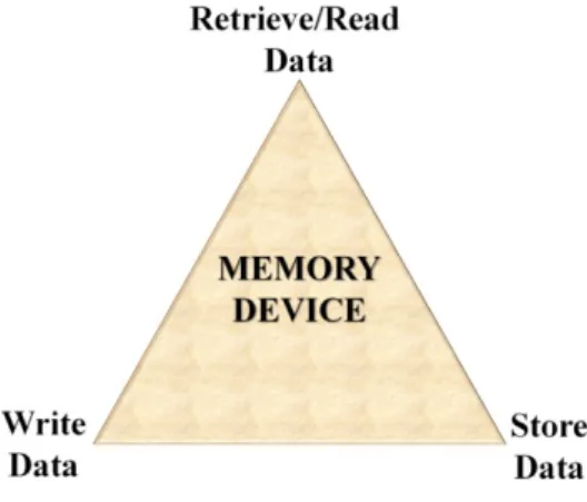
As shown in fig. 2, a memory device should follow at least three key requirements; (1)
The proposed device should be able to store information. If the information is stored for
long periods of time even without power, then it is called a non-volatile memory device.
(2) There should be mechanisms to read information from the device and (3) There
should be mechanisms to write information onto the device. To achieve these
requirements in MRAM, researchers have designed and investigated various kinds of
MRAM schemes in the past. In MRAM, these functions are performed as following: i)
The read operation is carried out by sensing the resistance difference between two states
of a magnetoresistive device. ii) The storage of information relies on the magnetic
retention properties, arising from the magnetic anisotropy of storage layer. iii) The write
operation is performed by changing the orientation of storage layer magnetization, which
can be achieved by inducing a magnetic field, or by using the principles of STT.
The first storage element used in MRAM for storing information was based on spin valve
structure, which mainly consisted of two ferromagnetic layers sandwiching a
non-magnetic conductive layer. The two ferronon-magnetic layers are called the free/soft layer and
the hard/pinned layer, respectively. An antiferromagnetic (AFM) layer is used in
proximity of or in contact with the pinned layer in order to pin the magnetization
direction of the layer, which should not be reversed during the operation of the memory
two antiferromagnetically coupled layers to reduce the stray field, which may affect the
free layer (FL) stability. Although a pinned layer is mainly used in in-plane MRAM, we
use pinned layer to refer to the fixed layer or reference layer of a perpendicular MRAM.
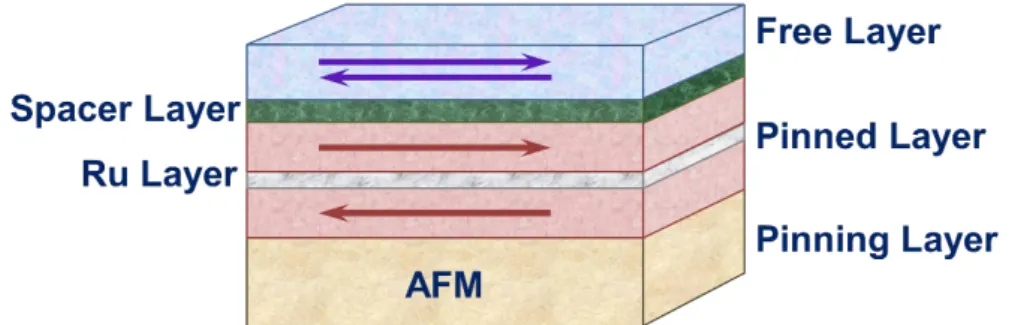
In MRAM designs, which involve a synthetic antiferromagnetic layer, the
antiferromagnetic coupling is induced by a thin ruthenium layer as shown in Fig. 3. The
ruthenium layer induces a strong antiferromagnetic exchange coupling between the two
magnetic sub-layers[37]. As a result, the synthetic antiferromagnetic layer helps to cancel
out the magnetostatic field from the pinned layer onto the free-layer [38-40]. Although
the spin valve devices had been used for the first MRAM memory’s research studies, they
still suffered from their low reading signal.
Figure 2 Three key requirements of a memory device
With the high reading signal found in magnetic tunnel junctions (MTJ), research interest
in spin valves decreased strongly. The MTJ structure is similar to spin valves, except that
the non-magnetic spacer is replaced by an insulating layer, which is also called as tunnel
barrier. MTJ is the predominant storage element in MRAMs for the past decade. The
current MRAM products use MTJs because the difference between the resistance states is
significant enough to produce the voltage swing required for application. An MTJ cell
(pinned layer and free-layer). Similar to a spin valve, the resistance states can be high
(antiparallel orientation) or low (parallel orientation) based on the relative orientation of
magnetizations of pinned layer and FL. The writing mechanism, to change the relative
magnetization orientations in the MTJ, is explained in section 3.3.
Figure 3. Schematics of spin valve structure used in read-sensors of hard disk drive and in
the initial investigations of magnetic random access memory.
A memory device should provide at least two states “bit”, so that they can be assigned to
digital signals of “0” and “1”, respectively. In the case of spin valves and MTJs, the
resistance states of these devices are different when the magnetizations of the two
magnetic layers are aligned parallel (low resistance) or antiparallel (high resistance) to
each other. These observations in spin valves and MTJs are called GMR and TMR),
respectively. These mechanisms are discussed in details in section 3.2.
The storage principle of an MRAM is based on the energy barrier required to switch the
magnetization of a single-domain magnet from one direction to the other (Fig. 4). The
magnetization will be fixed in a particular direction, if the energy barrier for
magnetization reversal is high enough to overcome the external stray fields and the
thermally assisted reversal of magnetization. This storage principle is very similar to that
used in magnetic recording, although the way the materials are designed and the
Figure 4 Relative energy barriers of free layer and fixed layer in a magnetic tunnel
junction. Both EB1 and EB2 are much larger than the thermal energy kBT
In an MRAM, the magnetization direction of the reference layer (or PL) is fixed and only
the magnetization direction of the free layer (FL) varies to store “0” and “1” states. Since
the direction of the reference layer must never be changed, it is made of materials, which
have a huge energy barrier. The free layer is designed with materials that have a magnetic
anisotropy, just sufficiently high enough to store the magnetization for certain years
(typically 10 years in the case of magnetic recording). The energy barrier that helps to
store the information is typically proportional to KuV (where Ku is the magnetic
anisotropy constant and V is the volume of the free layer). This energy must be much
larger (60 times, for storage time longer than 10 years) than the thermal energy kBT. In
certain cases, the energy barrier EB may be of different from KuV and hence, the thermal
stability factor is simply written as kBT). Although a high anisotropy is preferred
for storing information, the anisotropy of these materials cannot be too high, as their
magnetization direction needs to be oriented at will, to write 0 and 1 states. Based on the
has magnetization of ferromagnetic layers in the film plane and (ii) perpendicular MTJ
having the magnetization perpendicular to the film plane [41].
4. Reading in MRAM : Magnetoresistance
As discussed in the previous section, being able to read information is one of the three
important criteria. The magnetoresistance (MR) effect is the key to read information
reliably. The voltage difference between the low resistance state and the high resistance
state must be above 0.2 V, in order to read the information reliably. Therefore, it is
essential to achieve a high magnetoresistance to make the MRAM more reliable. This
section talks about the magnetoresistance in detail.
W. Thomson first observed magnetoresistance in pieces of iron and nickel in 1856. His
observations were based on the changes in the resistance of iron and nickel, when the
orientation of magnetic field was altered [42]. The MR effect arises due to the spin-orbit
coupling. The change in orientation of magnetization deforms the electron cloud slightly,
resulting a change in the amount of scattering of conduction electrons travelling across
the lattice. This change leads to different resistance values when the orientation of
magnetizations is different. The MR effect depends on both strength and relative direction
of the magnetic field. MR effect has also been reported in non-magnetic materials like In,
Al, Sb, Mo, Cu, Au, Pt, and others, but it is saturated at different specific conditions [43].
In materials like ferromagnets, MR effect of 2% order has been reported and it is
anisotropic in nature. Hence, it is called anisotropic magnetoresistance (AMR) effect. The
hard disk drives, due to its relatively large effect at room temperature and low saturation
fields, in comparison to the inductive head technology [44-46]. The change in resistance
of AMR in polycrystalline ferromagnets like (Ga, Mn)As depends on the angle between
the magnetization and current density [47].
The magnetoresistance value got a significant enhancement when sandwich structures
containing ferromagnetic (Fe) layers and a thin non-magnetic film (Cr) were investigated.
This new effect that caused an enhanced magnetoresistance is known as GMR effect, and
was discovered by Albert Fert and Peter Grünberg independently in the late 1980s. The
application of GMR in the reading head made a revolutionary change in the hard disk
drives as a high GMR lead to a high reading signal. Albert Fert and Peter Grünberg
received Nobel Prize in Physics (2007) for this effort.
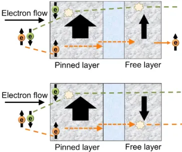
Figure 5. Illustration of spin dependent conduction in spin valve. The bold arrows
indicate magnetization states of pinned and free layers. The arrows with e indicate the
electron spins. The scattering of electrons is higher when the magnetizations of the two
The enhanced or so-called ‘giant’ magnetoresistance effect is a consequence of spin
dependent scattering. When the magnetizations of two layers of neighboring magnetic
layers are aligned in anti-parallel direction, both the minority and majority electrons get
scattered (Fig.5). As a result, a high resistance is observed. However, a drop in resistivity
is observed when magnetic orientations of ferromagnetic layers are parallel to each other.
This is because, for parallel orientation of magnetization, the majority electrons are
scattered less in comparison to the minority electrons.
The GMR effect also has been observed in multi-stacked films like Co/Cu, Ni/Fe, Fe/Au
and others. The Co/Cu and CoFe/Cu show high MR [22, 23, 48-53]. Although GMR was
an interesting observation, it was not directly applicable to hard disk drives, as the effect
requires a field larger than those produced by a magnetic medium. The invention of spin
valves (discussed in section 3) helped to solve the problems of GMR and make spin valve
a suitable magnetoresistive device for hard disk applications. The maximum GMR of 61
% was observed in the ballistic Co/H2Pc/Co junction [54]. Although, the practical GMR
observed for reading head application has remained about 10% ~ 20% [55, 56]. This
change was not significant enough to produce a significant voltage difference between the
high and low resistance states. Therefore, GMR is not of practical interest in MRAM
applications.
TMR, which was first reported at room temperature, by Moodera et al. and Miyazaki et
al. in 1995 was a major boost for MRAM applications [24, 25]. They reported TMR
values of about 16% at room temperature, which was very high at that point of time.
Moreover, the fact that the TMR was reported at room temperature was a great leap. The
amorphous AlOx was the insulating layer that they used in the magnetic tunnel junction
[24, 25, 57]. Since then, several developments such as the use of MgO crystalline barriers
demonstrations. At the point of writing, TMR values of 100 ~ 200% are readily achieved
in MRAM devices, which provide sufficient voltage difference between 0 and 1 states.
In MTJ for TMR, two ferromagnetic layers sandwich a very thin insulating film, typically
a few atomic layers thin, so that electrons can tunnel through the insulating layer
depending on the available free electron states on the ferromagnetic layer. In the
advanced MTJ devices with MgO tunnel barrier, the TMR also depends on the band
matching nature of the interfaces. Unlike GMR, where the resistance is caused by
spin-dependent scattering, the resistance difference in TMR is caused by spin-spin-dependent
tunneling. When the magnetizations of the layers are aligned parallel, more majority
electrons tunnel through the barrier. However, when the magnetizations of the layers are
aligned antiparallel, the probability of tunneling for both the majority and minority
electrons is reduced, resulting in a higher resistance. The resistance difference of different
magnetic orientations is measured by the TMR ratio, which can be calculated by the
following:
TMR ratio=Rap−Rp Rp
, (3)
where, Rap and Rp are the resistances of antiparallel and parallel relative orientation of free-layer and the reference layer, respectively.
The insulating barrier in the MTJ and the design of the whole stack, decide the TMR and
the reading performance of an MRAM. In the case of an amorphous barrier, such as
AlOx, the tunneling depends mainly on the electronic band structure of the ferromagnetic
materials. A maximum value in TMR of 70% was achieved using AlO [58]. However,
when crystalline barriers such as MgO, with crystalline and band matched magnetic
matching. Consequently, majority electrons have a larger probability of tunneling for
parallel magnetization. However, for antiparallel magnetization orientation, the
probability of tunneling is very low for majority and minority electrons. This effect was
theoretically predicted by Butler in 2000 [59] and the experimental results, which involve
MgO started pouring in the middle of the 2000s [60-62]. Yuasa et al. and Parkin et al.
showed that the TMR of MgO based MTJs can be greater than that of AlO barriers [60,
63]. In the same year, Djayaprawira et al. demonstrated TMR ratio higher than 200% in
CoFeB/MgO/CoFeB MTJ [61]. The TMR achieved using MgO gradually increased to
record high values of about 1000% at low temperature [64, 65] (Fig. 6).
Figure 6 Evolution of Tunnel Magnetoresistance (TMR) (%) from references [24, 25,
66-73], (a)[64], (b)[65], (c)[74], (d)[62], (e)[61], and (f) [75]. Slower growth was observed in
the case of amorphous barriers such as AlO. The rapid growth in TMR has occurred since
the introduction of crystalline barriers such as MgO with band-matched structures (red
Designing of MTJ is crucial in achieving a high TMR. In the case of MTJs with MgO
crystalline barrier, it is essential that the MgO layer has a (001) texture. This
crystallographic texture provides the band matching and the highest TMR. It is also
essential to design the magnetic materials at both sides of the MgO layer to have a (001)
texture. In the fabrication of MTJ stack, the most common interface is of the type CoFeB/
MgO/CoFeB. The CoFeB layer is amorphous in the as-deposited condition. When MgO
is deposited on such an amorphous layer, it develops a (001) texture under suitable
deposition conditions. However, one needs a crystalline interface for high TMR. To
achieve a crystalline CoFe with a (001) texture, the MTJ is annealed at a temperature of
about 300oC. During the annealing, B migrates out of CoFeB layer and the MgO (001)
texture helps to achieve a (001) texture in CoFe. When forming the MgO based MTJs,
one must be careful to avoid CoFe(111) texture. The presence of CoFe layers with a (111)
5. Writing Methods for MRAM
The second requirement of the memory device is that there should be a method to write
data in the memory cells. The writing in MRAM has been evolving and is achieved using
different methods in the past and in the recent past. One of the oldest methods used to
write information is based on applying a magnetic field, generated by current carrying
wires. According to Biot-Savart law, a current carrying conductor will generate a
magnetic field. This principle was used until a decade back, to achieve writing (also
called switching of magnetization or simply switching). In this method, the MRAM
architecture consists of bit line and word line (Fig. 7). When a current is sent through the
bit line and word line corresponding to a particular MRAM cell, two magnetic fields are
produced orthogonal to each other (Fig. 7(a)). The current in the word line generates a
magnetic field HW along the easy axis, and the current in thebit line generates a magnetic
field HB in transverse direction to the easy axis. Since field-assisted MRAMs were
developed with in-plane magnetization, the easy axes in such MRAMs lie along the
longer axis of the ellipsoid cells. It is worthy to mention that STT-MRAM architecture (to
Figure 7 Schematic of conventional MRAM based on magnetic field induced writing and
the selection process involved in the selection of a particular MRAM cell. Only the
free-layer of selected MRAM cell will switch, due to a higher applied total magnetic field.
Under the Stoner-Wohlfarth switching mechanism, the threshold field required for
resulting in magnetic field switching is given by
HW+HB=HK
2
3 (1)
where HK is anisotropy of the single domain magnet under consideration (in the case of
MRAM, the free layer part of the MRAM cell) [76]. The magnetic state of the free-layer
changes, when the resultant field strength exceeds the switching threshold (HK). It can be
noticed from this equation, for HW or HB not exceeding HK, that the switching occurs
only when the magnetic fields from both the currents are present and together they exceed
HK, satisfying equation (1). This helps in the selection of the preferred MRAM cell and
Figure 8 A comparison of the architecture of MRAMs with (a) field induced switching (b)
Spin Torque Transfer (STT) switching. In STT switching, the current is sent through the
MTJ and the resultant structure is much less complex than that of field MRAM.
The current required for generating the magnetic field depends on the magnetic and
morphological properties of the storing element. The switching field is inversely
proportional to the area of the storing element. As a result, scalability towards smaller
dimensions becomes a problem, since a higher current is needed to achieve a higher
switching field. The scalability of field-assisted MRAM is limited to about 90 nm, due to
a larger current required to induce the magnetic field in small cross section of wires [41,
78].
MRAM was almost given up by several researchers for a short while, as the field-based
switching was found to be not scalable to smaller dimensions and there was no clear
indication of an alternative. Thermally assisted MRAM, which relies on the joule heating
and exchange coupling between an antiferromagnetic material and a ferromagnetic
material to improve thermal stability was proposed in 2000s [79, 80]. This technology is
still being pursued by a few groups, although STT based switching is much widely being
Nevertheless, the proposal on STT based switching for MRAM revived the research
interest and the subsequent commercial interest [81-84].It is surprising that the proposal
of STT-MRAM took almost a decade, even though the theoretical predictions were made
independently by Berger and Slonczewski in 1996 [26, 27]. The STT switching in
magnetic nanopillars was first experimentally observed by Katine et al. in 2000 [28]. The
first few proposals on STT-MRAM appeared in 2006 [85-87].
As shown in Fig. 8(b), STT method does not require any external magnetic field to switch
the state of magnetization. Rather, the switching of magnetizations is induced by sending
a current through the device. Interestingly, switching by current is scalable (figure 9),
which also simplifies the MRAM design (Fig. 10), and hence the fabrication process as
well. In the STT switching process, electrons are sent from pinned layer to free-layer, if
the magnetization direction needs to be changed from antiparallel to parallel. When the
electrons flow through the pinned layer, the minority electrons get scattered and the
majority electrons pass through to the free layer. This process of selectively transferring
one type of electrons as the majority is called polarization. When these polarized
electrons reach the free layer, the spin angular momentum exerts a torque on the
magnetization of the layer that is oriented antiparallel to the pinned layer as shown in Fig.
10 (a). As the result of this torque generated by several electrons, the magnetization
Figure 9. Required writing currents for switching of free layers in different types of
MRAMs for different cell sizes. The current required in the case of field MRAM
increases when the cell size decreases whereas that required by STT-MRAM decreases
with cell size [65].
When it is required to achieve an antiparallel magnetization configuration, the current
direction is reversed. In this case, the electrons are sent from the free layer towards the
pinned layer. The majority electrons pass through the interface and the minority electrons
are scattered back to the free layer. The transfer of spin angular momentum between the
reflected electrons and the magnetization results in an antiparallel magnetization
configuration (Figure 10(b)). The magnetic state of free-layer changes only when the
torque is strong enough. If the current is not enough, the magnetization may rotate and
revert back to its initial state. If the current is very large, the reversal may happen at a
faster rate, but this leads to a significant power consumption (Fig. 11). The critical current
Jc is needed to reverse the magnetization of the free-layer and the critical current density
Jc is given by [26]
Jc=
(
α η)(
2e
where Ms is saturation magnetization, t is thickness of the film, and α is the Gilbert
damping constant, which represents the rate at which the magnetization relaxes to its
equilibrium position. The parameter η in above equation is theSTT efficiency parameter,
which is related to the spin polarization of the injected current.
Figure 10 Schematic illustration of an STT-MRAM cell and the STT switching
mechanism to achieve 1 and 0 states. The bold arrows indicate the magnetization states of
Figure 11 Precession of the spin in switching state for a)J=¿ Jc and b) J≫Jc. The blue
line shows the trajectory and the bold arrows show the initial and final states of
magnetization. The dotted line shows an intermediate state of magnetization
6. Storage methods and choice of materials
Based on the storage methods, MRAMs can be classified into two categories; (1) In-plane
MRAM and (2) Perpendicular MRAM. In the case of in-plane MRAM, the
magnetizations of the reference and the free layers lie in the film-plane. In the case of
perpendicular MRAM, the magnetizations of the reference and the free layers lie
perpendicular to the film-plane. In this section, we will discuss details of these two types
of storage principles, materials and their advantages and disadvantages for MRAM
application.
6. 1. In-plane MRAM
In the earlier generations of MRAM and until recently, the storage layers used in MTJ
devices are in-plane magnetized. The main advantage of in-plane MRAMs are that they
are relatively easy to manufacture than their counterparts. Another reason for using
materials with in-plane magnetization was that the magnetic field produced in the
field-switching MRAMs were in-plane magnetic fields. Such fields are able to switch in-plane
magnetizations. The disadvantage of in-plane MRAM is that they are not scalable to very
high densities. This is mainly due to a continuous increase of the magnetostatic field as
the device lateral size shrinks. It is believed that this trend of using in-plane MRAM will
continue only for a few more years.
During early research on MRAM, materials such as Fe, NiFe, Co and CoFe were used in
curling at the edges of the films. This magnetization curling leads to the formation of
vortex magnetization in the films. In order to prevent this vortex formation, the aspect
ratio (length/width) of these films was designed to be more than or equal to 2. The aspect
ratio also provides a direction for the easy axis of magnetization along the major axis, due
to shape anisotropy. However, due to scalability concerns, MTJs with elliptical shapes are
not desired as they take larger space than circular dots and hence decrease the density of
MRAM [88-90]. The curling of magnetization also causes the problem of anomalous
switching in in-plane MTJ [91-93].
In the current technology, CoFeB is used as the free layer in an MgO based MTJ. As
discussed earlier, thermal stability of STT-MRAM is a very important factor for its
functionality and long lasting performance. The data retention probability of MRAM
depends on the thermal stability of the MTJ. The thermal stability factor =Eb/KBT,
must be greater than 60 for retaining data for more than 10 years. For the uniform rotation
of magnetization, the energy barrier Eb is the anisotropy energy (KuV), where Kuis the
uniaxial anisotropy constant and V is the volume. Furthermore,
Ku=HKMs/2 (4)
(where HK is the anisotropy field and Msis the saturation magnetization). The thermal
stability factor can be defined as [24, 25, 79]
∆=HKMsV 2kBT
. (5)
For a storage life of 10 years, it is essential to have of about 60, which results in a cell diameter of 60 nm as the ultimate size for in-plane MRAM for materials such as CoFeB,
with a thickness of 5 nm and a Ku of about 8x 10⁴ ergs/cc. For sizes smaller than 60 nm, it
Besides the thermal stability of the free layer, it is also essential to achieve the thermal
stability of magnetization of the reference layer. However, the magnetization of the
reference layer has to be fixed at all times and it is not necessary to reverse its direction.
Shape anisotropy, associated with cylindrical shaped dots is one way to achieve a higher
anisotropy and coercivity for the reference layer. However, the achievable density is not
so high with this technique. Therefore, exchange bias is used as a technique to pin the
direction of the magnetic layer [94]. For this purpose, an antiferromagnetic layer such as
IrMn is deposited in contact to the reference layer. A magnetic field annealing is carried
out to pin the direction of magnetization of pinned layer. To achieve exchange bias, the
sample is annealed at a temperature above the blocking temperature (TB) of
antiferromagnetic layer and below the Curie temperature (TC) of the ferromagnetic layer.
At this temperature TB < T < TC, the antiferromagnetic material does not have its
anisotropy but the reference layer does have its magnetic ordering. When a magnetic field
is applied and the sample is cooled from this temperature, the magnetization of the
reference layer is oriented along the magnetic field direction. The magnetic moments of
the atoms of the antiferromagnetic layer in contact with the magnetic layer are also frozen
in this direction. As a result, the exchange coupling of the antiferromagnetic layer is also
set along this direction.
Devices fabricated using in-plane anisotropy materials for MRAMs are already available
in the market. However, thermal stability of in-plane MTJ for devices smaller than about
60 nm forces researchers to look for alternative technologies that will enable smaller
devices. As a result, the future of in-plane MTJ structure in MRAM is limited and there is
6. 2. Perpendicular MRAM
In the past decade, there has been significant amount of research in the field of MTJs with
a perpendicular magnetization (pMTJ). It has to be noted that the transition from
longitudinal to perpendicular magnetic recording technology for hard disk drives took
place when it was practically impossible to push the density of longitudinal recording
technology. Similar transition is expected to take place in MRAM, too, when it is not
practically viable to scale the current products based on in-plane MTJs.
A perpendicular magnetic anisotropy (PMA) enables magnetization to remain in the
direction perpendicular to the film-plane, whereas the magnetization direction for a film
without PMA is in-plane. Moreover, most films with a PMA have been found to have a
higher anisotropy constant. There are also additional benefits in writing mechanism,
arising from a PMA configurations. As a result, the research on PMA has been growing
in the recent past. The first few publications that advocated and demonstrated the use of
PMA configurations for MRAM applications are based on well-established PMA
materials once used in/considered for magneto-optic recording. A higher TMR of 50% in
perpendicular MTJ with GdFe/CoFe layers, as compared to the in-plane MTJ was
reported by Nishimura et al [95]. Alloys of transition metals like TbFeCo, GdFeCo were
also adopted to obtain PMA. However, these materials have drawbacks in the form of
corrosion. The oxidation of these materials is unavoidable and results in deterioration of
magnetic properties and hence it is a challenge to use such materials [95, 96].
Transition metals like Co, Fe, when formed as multilayers in combinations of noble
metals such as Pt, Pd, Au show PMA. For example, these layers can be used together as
multilayers possess large value of PMA close to 107 erg/cc [97-100]. These CoPd
multilayers have been used with FeMn as an AFM layer to induce exchange bias
constituting a structure, which was similar to the conventional in-plane spin valve [101].
Another structure called pseudo spin valve without any AFM layer was demonstrated
later, where the coercive properties of these films can be tailored by altering the thickness
of Co and Pd, and the number of periods. Even though the Co/Pd or Co/Pt multilayers
could be used as pMTJ candidates, they have two significant issues, when they are used
as free layers. (i) Their anisotropy and the damping factor is very high, the writing current
would be also high as can be revealed from Eq. (2) and will be discussed in next section.
(ii) They have an fcc (111) structure. As a result, when MgO is grown on them, the MgO
layer would not achieve the desired (001) texture and hence the achieved TMR would be
low (Fig. 5). A breakthrough was needed to realize the advantages of PMA in MRAM
and it came in the form of thin CoFeB layers.
It was surprising that the CoFeB, which was predominantly used for in-plane MRAMs
provided the much needed breakthrough for the pMTJs as well. It was pointed out in 2010
that MTJs based on CoFeB-MgO could show PMA when the thickness of CoFeB layers
is smaller than 1.5 nm, whereas for films thicker than that value in-plane anisotropy is
observed as usual [102]. It has been pointed out that both Ta and MgO are crucial to
achieve the interface anisotropy. Replacing Ta with Ru or other such material did not
yield promising results [103]. The crystallized pMTJ system with CoFeB-MgO has
shown TMR of more than 100%. The demonstrated film also exhibits good thermal
stability and low switching current. The annealing process is a crucial step for PMA of
the CoFeB layer to get good TMR, low resistance and low critical current density [104].
The TMR value of CoFeB degraded as the thickness of CoFeB decreases, so the
widely believed that the first generation of pMTJs will be made using thin CoFeB based
MRAMs.
6. 3. Thermal Stability
Irrespective of whether Co/Pd multilayers or the thin CoFeB based MTJs are used for
MRAM applications, the thermal stability of magnetization is important to store the
information for longer periods without self-erasure. In the case of pMTJs, a free layer
with an anisotropy constant in the order of 1×10⁷ erg/cc is required for future. For a
thickness of about 5 nm, such material can support cell diameter around 10 nm, at
operating temperatures of about 70℃.
For perpendicular MTJs, the anisotropy arises from different sources and there are several
notations describing each contribution. When the PMA arises from a magnetocrystalline
anisotropy, this is denoted as the bulk anisotropy energy density Ku bulk
. If the anisotropy
arises from interfacial effects, this is called as surface anisotropy energy density σ. It
must be noted that the densities are with respect to volume and area in the case of bulk
and surface anisotropies respectively. The shape anisotropy energy density KD, arising
from the geometrical shapes of the devices, goes against the PMA and tries to keep the
magnetization in-plane. For the unpatented films and large devices (about a m), KD is
given by KD = −2πMs
2
. The value of HKi.e. field anisotropy field also varies for different
types of PMA.
For bulk-PMA, the anisotropy field is given by,
HK=2Ku bulk
For interfacial-PMA, the anisotropy field is given by,
HK= 2σ
MSt−4π MS (6)
By using the above equations the thermal stability factor ∆ for PMAs can be written as
follows:
For materials with a magnetocrystalline anisotropy,
∆=(Kubulkt−2π MS2t)πAR ω
2
4KBT
(7)
For materials with an interfacial anisotropy,
∆=(σ−2π MS2t)πAR ω
2
4KBT
(8)
where AR is the aspect ratio (length to width), ωthe width and t the thickness of the cell
[32, 102, 105].
For in-plane cells of elliptical shape, the anisotropy field is given by
HK=24π MS(AR−1)
ωAR (9)
and ∆ is given by
∆=π
2
(
MSt)
2
ω(AR−1)
KBt
(10)
In essence, in MRAM devices based on materials with a PMA arising from
increasing the thickness of the film (for a fixed diameter). However, in the case of PMA
based on interface anisotropy, it is not possible as the interface anisotropy is the major
factor in thermal stability. Any increase in thickness, leads to a reduction in thermal
stability as per the second term of equation 8 and also the loss of PMA.
One way to overcome the thermal stability issues of interface PMA based MTJs is to find
out alternatives, such as multilayers, which would increase thermal stability with
thickness. CoFeB/TaN based multilayers have been proposed as potential
candidates[106]. Another possibility is to use dual interfaces, such as
MgO/CoFeB/Ta/CoFeB/MgO, instead of Ta/CoFeB/MgO alone. In such dual-pMTJs,
both the layers of CoFeB are sandwiched by a layer of Ta and MgO and hence both
develop a perpendicular magnetic anisotropy. As the thickness of each layer can be about
1 nm each, the thermal stability is increased. Sato et al. have reported the increase of
thermal stability in such double interface structure by a factor of 1.9 from the highest
value of perpendicular MTJs with single CoFeB-MgO interface structure [107].
To increase the storage density, multi-level MRAM has been reported using complex
magnetoresistive spin valve with perpendicular anisotropy [108]. The structure consists of
two FLs and one reference layer, all based on Co/Pd multilayer exhibiting different four
resistance levels. The selection of free-layer for storing data can be done by distinct level
of resistance and their respective STT switching current [109].
As discussed earlier, spin-torque transfer (STT) principle has been widely accepted as the
method to write information. Any new methods implemented in the design of MRAM
must improve the writing speed, reduce the writing current and consumed power. This
section discusses, in detail, the methods in which writability or speed can be increased.
Equation (2) indicates that the critical current to switch the magnetization of the free layer
depends on the damping factor Therefore, it is essential to find materials that have a low damping factor, in order to reduce writing current. Materials such as FePt or Co/Pd,
which were once researched for pMTJ applications due to their high Ku, have a large
damping factor. Therefore, even though these materials could be scaled down to smaller
devices with high thermal stability, writing information on these devices would consume
significant power. In this context, the invention of interface-pMTJ based on
Ta/CoFeB/MgO came as a boon for the STT-MRAM. CoFeB has a much lower damping
factor and could be written with much lower currents, as compared to FePt or Co/Pd.
Interface-pMTJ devices could be used down to 20 nm sizes, beyond which one may
consider materials such as Co/Pd, Co/Pt or FePt, although the writing issues on such
materials should be solved. It is important to mention that Co/Pd or Co/Pt multilayers
have to be used in combination with other materials such as CoFeB for example for better
matching with MgO in term of crystal structure.
Another way to reduce the writing current in STT-MRAMs is to increase the spin-torque
transfer efficiency ( denominator in equation 2). One way to improve the spin-torque transfer efficiency is to increase the spin polarization of the materials used. CoFeB with a
reasonably high spin polarization is used at the interfaces of MTJ, even if materials such
as Co/Pd are used as the reference layers. Heusler alloys, with a much higher spin
using dual MTJs with two reference layers and one free layer [111]. An MTJ with double
tunnel barrier and two reference layer was reported by Hu et al.[112].was reported to improve by two folds as compared to a single MTJ with same resistance-area product
(RA).
Orthogonal spin-transfer magnetic random access memory (OST-MRAM) has been
proposed to increase the speed of magnetization reversal. This technology uses a
spin-polarizing layer magnetized perpendicularly to a free layer to achieve large spin-transfer
torques and ultrafast energy efficient switching. Reliable switching has been observed by
the researchers at room temperature with 500 ps pulses, indicating high-speed switching
in the range of 2 GHz. The switching has been reported to require an energy of less than
450 fJ [113, 114].
Magnetic nano-contacts are another alternative to increase writing efficiency. Sbiaa et al.
studied the STT switching in perpendicular free-layer with magnetic nano-contacts and
found a strong dependency of switching time on the size of nano-contact, as time reduces
from 1.6 ns to 0.8 ns by decreasing the size of the nano-contact. The value of critical
writing current and switching time was found to be less for fewer numbers of
nano-contacts compared to those with larger number of nano-nano-contacts [115].
The tilting of the free-layer with respect to the reference layer in perpendicular MTJ can
also increase the writing performance of MRAM in terms of switching time and
switching current [116]. As reported, for a tilt angle of 5°, switching speed of free-layer is
improved by 30% and switching current is reduced by 36%. The critical current density
Fast switching speed is one of the advantages of STT-MRAM. In comparison to its rivals
such as resistive RAM or phase change RAM, the STT-MRAM is 100x faster. The
switching speed is directly proportional to the switching current and inversely
proportional to the RA. Therefore, it is essential to reduce RA in order to improve the
speed of MRAM. RA is usually reduced by making thinner MgO barriers. However, this
must be achieved without sacrificing the tunnelling magnetoresistance. High switching
speed can also be achieved by applying high switching current Ic, which is achieved by a
high bias voltage applied across the device. It has been reported that the combination of
both (high current and a thinner barrier layer) can result in the breakdown of the AlOx
layer limiting the lifetime of MTJ [41]. The MgO layer, used in current products, is more
advantageous compared to AlO, as it hasa higher breakdown voltage, which increases the
lifetime of theMTJ. Moreover, MgO ishighly spin selective, which results in a large STT
and TMR effect, and it induces very high perpendicular magnetic anisotropy (PMA).
The Damping factor α, plays a major role in the switching speed of the devices. When a
magnetic field or spin torque current is applied, the magnetization precesses and changes
the direction (Fig. 11). This reversal time depends inversely on the damping factor. The
damping factor, α of magnetic materials depends on both intrinsic and extrinsic factors.
The intrinsic factors are mostly related to spin-orbit interaction. The spin-orbit
interaction varies with the atomic number (Z) of magnetic materials. A magnetic material
with a high value of Z has high spin-orbit interaction, which leads to a high value of α
[117, 118]. The CoFeB film has been reported to have low value of α = 0.001 0.1, as it contains only low Z elements [119]. The extrinsic factors include energy dissipation via
interaction with adjacent layers or dissipation due to scattering from the interface [120,
121]. These factors depend on the film roughness, thickness, growth method and coupling
compared to the bulks [102, 122]. It has to be mentioned that the value of α also defines
the switching current in STT and thermal magnetic noise for TMR head [26, 27, 123]. A
high α, which leads to faster switching might lead to undesirable effects when it comes to
writing current.
It can be noticed from the previous discussions that the damping factor plays
contradicting roles in the performance of writing current and writing speed. Afree layer
with a higher damping factor leads to the desired higher speed, but also results in a
requirement for higher writing current, which is not desired. Piramanayagam et al., have
proposed a design where the free layer consists of two layers, one with a high damping
factor and another with a lower damping factor. Depending on the combination of the two
damping factors and the coupling between the layers, writing current and speed may be
optimized[124].
In multilevel MRAMs discussed in the previous section, it is a challenge to switch a
particular layer to achieve the desired bit. Such a problem can be solved by introducing
STT from an oscillating layer. The use of oscillating layer is also reported to address the
particular layer to be switched and to reduce the switching time in the conventional MTJs
[109]
In order to improve the writability and read-signals, alternative materials are also sought.
One such system of materials is Heusler alloys. The interest in the Heusler alloy thin
films is widely increasing due to properties like tunable anisotropy, large spin
polarization and high Curie temperature, making them attractive for spintronic
applications like high density magnetic storage, STT-MRAM and magnonic devices [65,
been obtained in 53 nm thick Co2FeAl corresponding to an optimum substrate
temperature of 300 C [128]. Such low value of damping constant inspires the application of Heusler alloys in MRAM. Besides for the writing application, use of Heusler alloys
have also been reported for reading improvement due to large magnetic moments, 100%
spin polarization and the high Curie temperature [129, 130].The reading signal of an MRAM can be improved by increasing the magnetoresistance ratio. Investigations to
improve the magnetoresistance ratio using Heusler alloys for read sensors have also been
explored. A GMR ratio of 74.8 % has been already reported by Sato et al. using a
junction consisting of Co2Fe0.4Mn0.6Si/Ag/Co2Fe0.4Mn0.6Si [131]. On the other hand, a
TMR ratio of 386 % has been reported for Co2FeAl0.5Si0.5 at room temperature [132].
Moreover, researchers have predicted the TMR ratio of 1000 % within next 10 years
[133]. However, the path of obtaining the half metallicity in Heusler alloys films confront
obstacles such as the atomic displacement, misfit dislocation, and symmetry break in the
vicinity of the surface of the films. Nevertheless, once the half metallicity is achieved,
antiferromagnetic Heusler-alloy films can be combined with non-magnetic films to form
Heusler junctions, which may be used in MRAM. So far, this research is still in its early
stage
8. Reliability issues of MRAM
The reliability of the MRAM is the most important issue for its application. In 2004,
Åkerman et al. studied the reliability of 4 MB MTJ MRAM based on field-induced
switching. The device was found to be stable up to temperatures of 120 C in terms of dielectric breakdown, resistance drift and data retention. The life time of the device with
comparison to the field-switching MRAM, the STT-MRAM is more promising and hence
we have paid more attention in this section to the problems associated with it.
Regardless of the various advantages, STT-MRAM also confronts important challenges.
Although the write current is lower than in many other memory technologies, still it is
very high [135, 136]. Such high current leads to a high energy consumption [137, 138]..
Along with the issue of high-energy consumption, MRAM also confronts other failure
issues. The errors due to these failures can be categorized into fixable/correctable errors
or non-fixable/ non-correctable errors. The fixable errors occur due to the properties of
free-layer and can be fixed by sending the new signal. These errors are caused bythermal
fluctuations. The non-fixable errors occur due to the properties of the barrier oxide layer
and as their name suggests they cannot be fixed. These errors occur due to the voltage
breakdown of the MTJ or due to the waned TMR ratio under the impact of the bias
voltage [63, 102].
The fixable errors turn up to be due to the wrong signals. The data can be failed to be
stored due to areversal of the magnetization orientation caused by thermal fluctuations. It
can be avoided by increasing the writing current or duration of the current pulse. But,
these solutions can lead to the breakdown of the barrier oxide layer. Another possible
error can be due to erroneous reading, i.e. changes in the stored data while reading it. The
thermal stability factor is responsible for the data retention. The high value of reading
current or the longer reading duration can change the orientation of magnetization.
The non-fixable errors rise up due to the barrier oxide layer. The errors could be the
breakdown of the MTJ device limiting the life-time, which has been discussed earlier or
the waning TMR ratio under the influence of bias voltage. In order to get a low RA value,
TMR, which can disturb the sensing operations resulting in errors while reading the data
[136, 139-141]. Moreover, the write path itself is a challenge in MRAM. In
STT-MRAM, the read and write operations share the same access path (through the junction),
which damages the reliability such as mistakenly flipping the bit during the read
operation. Third, the long write latencies usually prohibit the use of STT-MRAM in first
level caches [142].
9. Emerging Memories
9.1. New Writing Schemes
9.1.1. Spin Hall Effect based Memory
Due to certain shortcomings of the STT-MRAM, alternative spin-based memories are
also being researched. One such candidate is Spin Hall Effect (SHE) based MRAM,
which promises lower power consumption in comparison to STT-MRAM. Spin Hall
effect is a phenomenon, where spin-orbit coupling leads to deflection of electrons of
different spin in different directions producing a pure spin current, transverse to an
applied charge current [143-149]. Pt was one of the first promising metallic materials
studied for the SHE, as it exhibits a substantial value of the effect, even at room
temperature [150]. The spin Hall conductivity in Pt at room temperature had been noticed
to be larger than the low temperature’s spin Hall conductivity of other metals like Al.
Such a high value of spin Hall conductivity arises from a high magnitude of spin-orbit
First SHE in Pt was interpreted to arise due to the side jumps, skew scattering and other
extrinsic mechanisms [152]. But later, studies of intrinsic mechanisms for such high
effect in Pt also have been done, which suggested the origin of this effect in Pt to be due
to intrinsic mechanisms [153, 154]. The use of SHE for MRAM with β-Tantalum layer
was reported by Liu et al. in 2012 [34]. In their experiment, the electric current sent
through a thin Ta layer, which induced spin torque switching due to SHE in the adjacent
ferromagnetic (CoFeB) layer for both, perpendicular and in-plane magnetized samples at
room temperature. The use of Ta was preferred over Pt due to the larger spin Hall angle
of Ta as compared to that of Pt, which gives a higher ratio of spin current density to
charge current density, arising from the SHE. Secondly, unlike Pt, Ta does not produce
damping in the adjacent ferromagnetic layer [155, 156]. The principle behind this is that,
due to SHE the oscillating current in Ta produces an oscillating spin current, which
enforces an oscillating spin torque on the magnetic moment of the ferromagnetic layer.
The performance of SHE MRAM (in-plane) and STT-MRAM (interface perpendicular)
based cache memory was comparatively studied by the J. Kim et al. using similar
material parameters and device dimensions with CoFeB as free layer [157]. The study,
based on simulations, reported that the SHE MRAM showed better results for critical spin
current, write delay, and retention failure rate (%) with respect to thermal stability. Y.
Kim et al. proposed a STT-bit cell based on SHE, suitable for high performance on-chip
memory, advocated by the 10 times lesser need of writing energy and exhibiting 1.6 times
faster reading time as compared to the 1T1R (One transistor one resistor) in-plane
Figure 12 Illustration of the path of write and read currents in (a) STT-MRAM and (b)
SOT MRAM. SOT MRAM uses separate paths for reading and writing information, as
shown by the arrows.
Besides low power consumption and faster switching, the use of three terminal
MTJ-based on spin orbit torque is also beneficial in isolating the read and the write path. In
spin orbit torque MRAM (SOT-MRAM), the read and the write paths are separated from
each other, which significantly improves the reading reliability [159]. Moreover, the write
current is much lower and also the write time is supposed to be much faster, as the write
path can now be optimized independently.
The MTJ cell is the core part of a bit-cell in SOT MRAM as in STT-MRAM. However, to
eliminate the shortcomings of STT-MRAM, the SOT MRAM cell has an additional
terminal to separate the (unidirectional) read and the (bidirectional) write path, which are
perpendicular to each other. The terminals comprise a bit line, a write line, a source line,
and a word line as shown in fig. 12(b). The word line is used to access the required cell
during the read operation. While in the write operation, the current flows between the
free layer and hence, the value stored in the bit-cell. If the current flows from the source
line to the write line, the MTJ resistance will be low. To achieve a high MTJ resistance,
the current needs to flow from write to source line (high potential for the write line)
[160].
Although spin-orbit torque is effective in achieving magnetization switching, the
underlying physical relation between the current and the magnetic field orientation is still
under discussion. Gambardella et al. and Miron et al., described Rashba effect to be a
cause of the current-induced magnetization switch [35, 161]. On the other hand, Liu et al.
attributed spin Hall effect to be the cause [34]. Nonetheless, irrespective of the actual
effect, the spin-orbit torque is responsible for the switching of free layer magnetization
and hence the name SOT-MRAM. Because of all the advantages of SOT-MRAM, it can
be a prominent memory to be used in the future. However, still more investigations on the
SOT-MRAM needs to be done to make it practical for commercial applications.
9.1 2. Electric Field Assisted Switching for MRAM
We have already mentioned that the writing process in the STT-MRAM using spin
polarized current is highly energy consuming. SOT-MRAM is considered as one
technology to reduce power consumption. Another efficient route to manipulate the
magnetization in MTJ is by using the voltage control of magnetic anisotropy (VCMA)
[162, 163]. In this scheme, a voltage is applied to a magnetic material/insulator interface,
which produces an electric field and changes the magnetic anisotropy of the material. The
power. Because of the promising potential of energy efficiency, the electric field assisted
switching of memory based on VCMA is catching lot of interest [164-168].
The first ever electric field control of ferromagnetic properties was demonstrated by Ohno
et al. in 2000 [169]. Later, modification of coercivity, magnetic anisotropy, and Curie
temperature by altering the carrier density with a gate voltage also were demonstrated
[169-171]. VCMA effect relies on electric field induced change of atomic orbital
occupancy at interface. This change is in synchronic connection with spin-orbital
interaction, which consequently results in the change of anisotropy [172-174]. A
qualitative explanation based on Rashba effect also has been given for VCMA, which
relies on the Dzyaloshinskii–Moriya mechanism[175].
In 2010, electric field effects on thickness dependent magnetic properties of CoFeB layers
was investigated at room temperature. This study demonstrated the electric field
manipulation of magnetic anisotropy in in-plane 2 nm thick CoFeB. On the other hand,
for 1.16 nm and 1.02 nm thick perpendicularly magnetized CoFeB electric field induced
alteration of coercivity was observed [176]. Wang et al. in 2012 demonstrated the
electric-field-assisted switching in perpendicular MTJs [177]. The usual MTJs have thick
ferromagnetic layers (>3 nm), where the magnetic anisotropy is independent of the
ferromagnetic barrier oxide layer interface [24, 25, 60, 61]. The electric field effect in
these layers is negligible due to the screening of electrons. In the case of electric field
assisted switching, the thickness of CoFeB is relatively thin (1.6 nm). For this thickness,
the PMA arises from the oxide layer interface. As a result of the applied field, the
interface anisotropy is affected and the magnetic orientation is changed [102, 177].
The main advantage of using the VCMA based memory is the dramatic reduction in

![Figure 6 Evolution of Tunnel Magnetoresistance (TMR) (%) from references [24, 25, 66- 66-73], (a)[64], (b)[65], (c)[74], (d)[62], (e)[61], and (f) [75]](https://thumb-us.123doks.com/thumbv2/123dok_us/7731488.162901/18.892.160.580.512.852/figure-evolution-tunnel-magnetoresistance-tmr-references-b-c.webp)