Implementation of Basic Gates and Compound
Gates (AOI & OAI) using Ladder Diagram in
Programmable Logic Controller (PLC)
Darshan Halliyavar1, Shwetha M P1, Puneeth S1, K. Sudha Deepthi2
Assistant Professor, Department of Electronics and Communication, School of Engineering, Daynanda Sagar
University, Bangalore, Karnataka, India1
Assistant Manager, Bosch Rexroth Innovation lab, School of Engineering, Daynanda Sagar University, Bangalore,
Karnataka, India2
ABSTRACT: Programmable Logic Controllers or PLC, normally a digitized controller is fixed, rigid and industrial digital computer. Earlier days in industry, electromechanical relays, timers, counters and sequencers were widely used. The drawback of using these are many with respect to cost, wiring, and maintenance is more. The advancement in PLC came up to overcome all these factors. The question why PLC is the tool, which gives the control and hold in automation, it provides high gain, improved quality and accuracy, works flexible in criticized and hazardous situation, increase product rate, early time to market, low cost, and mainly since the automation helps in designing and changing over easily from one product to another. In this work, we have designed and simulated the basic gates and compound gates using ladder diagram in PLC, using Indraworks, Indralogic platform. This paper forms a basic for designing complex sequential circuits and helps in developing VLSI circuits. This paper gives a overview of AOI(And OR Inverter) and OAI(Or And Inverter) circuits designed and simulated through PLC with the help of ladder diagram.
KEYWORDS: PLC, Indralogic, Ladder diagram, NMEA, AOI, OAI.
I. INTRODUCTION
A formal definition of a PLC comes from the National Electrical Manufacturers Association (NMEA): [A Programmable Logic Controller is] a digitally operated electronic system, designed for use in an industrial environment, which uses a programmable memory for the internal storage of user-oriented instructions for implementing specific functions such as logic, sequencing, timing, counting, and arithmetic to control, through digital or analog input and outputs, various types of machine or process.
First to see the for a device what would be Known as Programmable logic Controller.
Architecture:
Figure 1 Basic PLC architecture [9]
The Figure 1 shows the basic architecture of PLC. A Programmable Controllers is made up of following Sections: 1. Processor / Central Processing Unit: This is the brain, or microprocessor, which controls or supervises a
process according to the input CPU solves the user program and update the status of the outputs.
2. Programming Device: is the device where the programmer or operator can program or give instructions or data to the device to get desired output based on his application.
3. Input section: where the CPU gets the inputs from the devices such as, push button, limit switch or photoelectric sensors etc.
4. Output section: where the processed data from CPU to the devices such as lamp, motors conveyors etc. . 5. Communication Modules: it is an interface between CPU and I/O modules through which data flow from input
to CPU, CPU to Output, and Output Filed devices flows such as RS232, Profibus, and Ethernet etc.
Indralogic:
The Indralogic is the part of PLC which is completely software based. It comprises of different set of function modules which are available to integrate the Control topologies. It uses the high speed system bus which helps in the smooth operation of the PLC. It also ensures the control processor for the high requirement of performance and functionality.
II. RELATED WORK
III.SIMULATION RESULTS
AND:
Figure 2: Symbol, Truth Table and simulation of AND gate.
Above circuit is designed using ladder diagram in PLC. The two input AND gate is designed by using two input and one output node. The symbol ‘ǀ ǀ’ represents the input node. The input is normally closed for logic 1 operation and
normally opened for logic 0 operation. The symbol ‘( )’ represents the output node. The above circuit is tested for all the combinations of the AND gate and the simulation is shown for the fourth combination of the truth table as shown in the Figure 2.
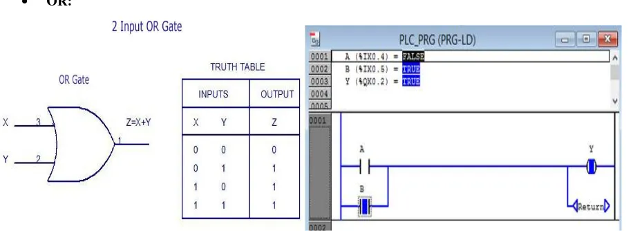
OR:
NAND:
Figure 4: Symbol, Truth Table and simulation of NAND gate.
The two input NAND gate is designed by using two input and one output node. The above circuit is tested for all the combinations of the NAND gate and the simulation is done for the first combination of the truth table as shown in the above Figure 4.
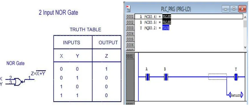
NOR:
Figure 5: Symbol, Truth Table and simulation of NOR gate.
XOR:
Figure 6: Symbol, Truth Table and simulation of XOR gate.
The two input XOR gate is designed by using two input and one output node. The above circuit is tested for all the combinations of the XOR gate and the simulation is done for the second combination of the truth table as shown in the Figure 6.
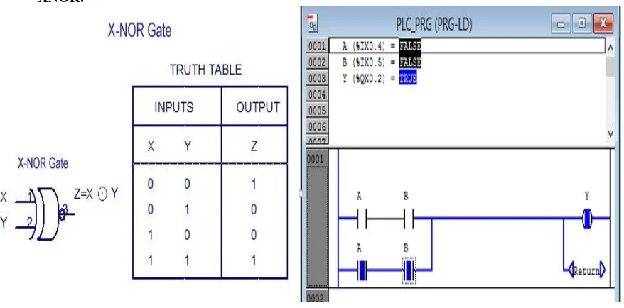
XNOR:
AND-OR-INVERT (AOI) and OR-AND-INVERT (OAI):
Figure 8: Symbol of AOI and OAI gate.
AND-OR-INVERT(AOI)/OR-AND-INVERT (OAI) gate belongs to Complex gates, It is designed by using combination of three basic gates AND, OR and NOT (Inverter) gates. Figure 8 depicts the symbol of AOI and OAI gates. AOI/OAI gate has many advantages instead of using individual gates. Since AOI/OAI is the combination of gates it greatly reduces area and power. The major advantage of using these gates is that the speed will be more and good efficiency and accuracy. The number of transistors used to design AOI/OAI will be less and hence it is used in low area and low power applications in VLSI.
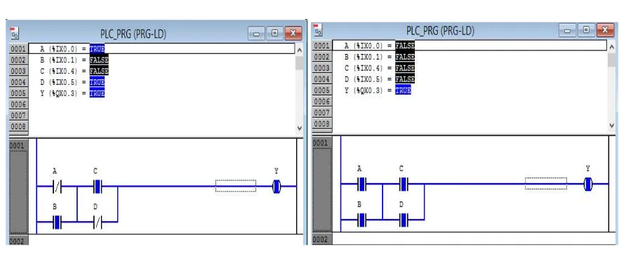
Simulation of AOI:
Figure 9: Simulation of AOI gate.
Simulation of OAI:
Figure 10: Simulation of OAI gate.
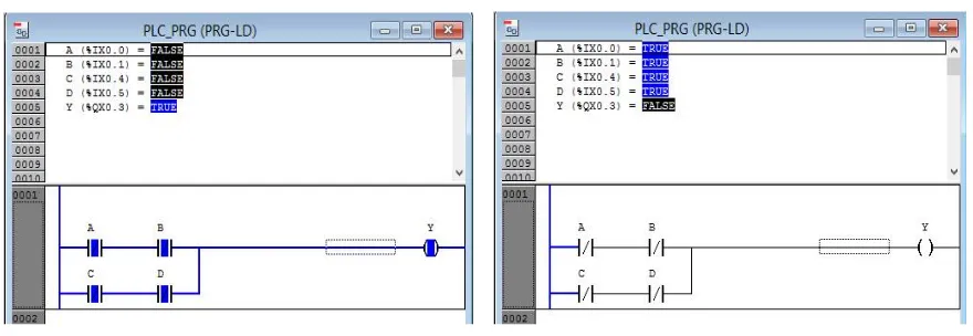
The 2-2 OAI gate is designed by using four input and one output node. The above circuit is tested for all the sixteen combinations of the OAI gate truth table. Figure 10 shows the simulation of OAI gate for two combinations. The first figure is shown for 0000 combination with output as 1 and second figure for the combination of 1111 with output as 0.
IV. CONCLUSION AND FUTURE SCOPE
In this work, we have simulated all the basic gates and complex gates using ladder diagram. Further work can be carried out using these basic gates in higher levels and can be implemented using ladder diagram. Different set of combinational circuits and sequential circuits can be implemented through ladder diagram. In future the digital circuits can be implemented with help of PLC through ladder diagrams.
ACKNOWLEDGEMENT
We want to thank the Dayananda Sagar University Management and our Dean Dr.A.Sreenivasan for giving chance to work with Bosch Rexroth Group. We thank our Chairman Prof Vaibhav.A for his guidance and motivation. We also thank Dr. Sanjay Chitnis, Director-Innovation and Entrepreneurship, SOE-DSU.
REFERENCES
1. Dr. Wai Phyo Aung, “Guidelines for Approching Steps of Learning Programmable Logic Controllers in Automation, International journal of Trend in Scientific research and development, ISSN 2456-6470/vol-2/Issue – 4
2. Dhruthi ane, etc..”Implentation of PLC using FPGA”, International of Journal of Scientific Engineering an Research, ISSN : 2347-3878 3. M. Hudedmani, R. Umayal, S. Kabberalli, and R. Hittalamani, “Programmable Logic Controller (PLC) in Automation”, Advance Journal of
Grad, Res, vol. 2, no. 1, pp. 37-45, May 2017.
4. Avvaru Ravi Kiran, B.Venkat Sundeep, Ch. Sree Vardhan, Neel Mathews, “The Principle of Programmable Logic Controller Automation”. International Journal of Engineering Trends and Technology- Volume4 Issue 36 pp 65-72.
5. Camel Yilmaz, “Implementation of PLC – Based Home automation”, Journal of Applied sciences, ISSN:1812-5654
6. L. A. Bryan, E. A. Bryan, “Programmable controllers: theory and Implementation”, 2nd ed., ISBN 0-944107-32-X, Industrial Text Company, 1997..
![Figure 1 Basic PLC architecture [9]](https://thumb-us.123doks.com/thumbv2/123dok_us/1374320.1170130/2.595.197.396.231.376/figure-basic-plc-architecture.webp)