VLSI Design of Efficient ML Detector for
MIMO Wireless Communication Systems
Rajasree P R1, Dr.S.Rajkumar2
PG Student, Dept. Electronics and Communication Engineering, Nehru College of Engineering and Research Centre,
Thrissur, India1
HOD, Dept. Electronics & Communication Engineering, Nehru College of Engineering and Research Centre, Thrissur,
India 2
ABSTRACT: The complexity of modern wireless communication system are increasing at fast pace. So it is critical to verify the design characteristics at the earliest possible stage to minimize costly design iterations. The MIMO wireless communication system consists of MIMO transmitter and MIMO receiver along with the along with a realistic fading channel. Detection and performance analysis of the system, mainly BER measurement is done in the demodulation section. So far we have ML detectors with heavy hardware. Here an efficient ML detection algorithm is proposed for the MIMO signal detection based on differential metrics. ML detector with a control mechanism is proposed which can reduce the computational complexity. By reducing the number of multiplication operations, a low complexity ML algorithm, is proposed for efficient detection for MIMO wireless communication. The ML detector designed using VHDL coding, it is simulated in Model SIM 6.2b, synthesized using Xilinx ISE 13.1 for area and power analysis, and implemented in SPARTAN 3E which is connected with MATLAB R2013a through UART port. The proposed design achieves 85.22% reduction in power, 67.30% reduction in area and 4.85% reduction in delay, while compared to existing ML design. And the new design still gives a lower BER measurement.
KEYWORDS: Additive white Gaussian noise (AWGN); Bit-error rate (BER); Maximum likelihood (ML); Multiple input multiple output (MIMO); Field programmable gate array (FPGA).
I. INTRODUCTION
The extensive demand for increasingly sophisticated connectivity, anytime, anywhere, made the wireless communication, one of the widest and rapidly growing field in telecommunication industry. MIMO transmission techniques become the significant advancement in wireless communication. And the complexity of modern wireless communication system are increasing at fast pace. It becomes challenging to design the hardware of wireless system. But VLSI design techniques are nowadays capable of providing a powerful platform for those complicated designs.
1) Many modern techniques, such as multiple-input–multiple-output (MIMO) systems, rely on computationally intensive signal processing at the receiver. Therefore, bit-true software-based simulation of these algorithms on workstations is becoming prohibitively time consuming. In addition, for a communication system specification with a set of target system requirements such as data throughput, received power, available bandwidth, noise statistics, and a target error performance, there are typically various potential solutions.
An efficient model of ML detector is designed to reduce the computational complexity of conventional method. The synthesis results from Xilinx ISE 13.1 of the proposed system are compared with the conventional ML detector and also with the existing ML detector [1] which is from IEEE transaction on VLSI system 2013.
II. RELATED WORK
The maximum likelihood (ML) detection problem for the linear multiple input Multiple-output (MIMO) channel was investigated in the context of CDMA after it was shown that an optimum detector offered a Significant gain in performance over conventional symbol by symbol detectors. In the context of CDMA the problem of optimal detection is usually referred to as optimal multiuser detection (MUD) since in this scenario the ML detection problem corresponds to the simultaneous detection of several users' symbols in the presence of multiple access interference.
More recently, similar detection problems have also been addressed when studying the joint detection of several symbols transmitted over a multiple antenna fading channel. The ML detection problem is known to be NP-hard. This implies that, unless there is some additional underlying structure in the problem considered, no known algorithms for its solution are of polynomial complexity in the number of symbols jointly detected. The most common class of suboptimum detectors is the class of linear detectors. These detectors apply a linear transformation to the received symbols prior to performing symbol by symbol decisions. The linear detectors include the zero-forcing (ZF) or decorrelating detector and the minimum mean square error (MMSE) detector. A more advanced class of detectors is given by the class of decision feedback (DF) detectors. These detectors make decisions on one symbol at the time and then subtract the contribution of this symbol on the remaining symbols prior to the next detection. In these detectors, the order in which the symbols are detected will strongly affect the performance of the detector. Typically, there is a tradeoff between computational complexity and accuracy of the above detectors. An efficient design and implementation of a parameterisable baseband MIMO BER measurement system on an FPGA, have been proposed with hardware modeling of ML detector [1].
III.PROPOSED DESIGN OF ML DETECTOR
An efficient design and implementation of a parameterisable baseband MIMO BER measurement system on an FPGA, can be made with hardware modeling of ML detector [1]. It used channel coefficients of a 2x2 MIMO communication for designing the detector. For avoiding number of iterations which include several multiplicative stages, a control unit can be included in the hardware. This control unit generates a differential matrix based on difference between received signal and channel coefficients. This is compared with received signal, it is preferred to have a higher value for received signal. If it is not, then the control unit goes for taking new input values by skipping multiplicative stages.
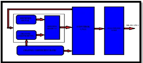
IV.BLOCK DIAGRAM
Here channel coefficients are stored in a memory and it is given as input to both computation and control modules. Control unit determines whether multiplicative stages are to be computed or else detected signals are to be checked again as next iterations. Fig. 1 shows the block diagram of proposed ML detector.
V. SIMULATION RESULTS
The hardware is modeled using VHDL coding. Channel coefficients are included in coding. Simulation results are verified in Model SIM 6.2b. Then the design is synthesized and implemented in Xilinx ISE 13.1, using SPARTAN 3E. The design summary from the synthesis is analyzed for area. And total power is analyzed. The results are compared with conventional ML and existing ML detector [1], which is again designed, simulated, and synthesized using same software. Design summary of conventional, existing, proposed ML detector is given and also the total power consumption too.
1. Design summary
Design summary of conventional, existing, proposed ML are provided by Xlinx ISE 13.1 for the synthesis and implementation in SPARTAN 3E.
Fig. 2. Design summary of conventional ML detector.
Fig. 3. Design summary of existing ML detector.
Here it is given that 433 slices of FPGA are to be utilized for conventional ML detector, 54 slices for existing design of ML detector and only 17 slices for the proposed design. That means, 96.07% reduction in area comparing to conventional design, and 67.30% reduction in area comparing with existing design.
2. Power summary
Power summary of the three designs are given. Conventional ML detector have a power consumption of 1.185W. Existing design consumes .203W in total. And for proposed design it is .031W.
Fig. 5. Power of conventional ML design
Fig. 6. Power of existing ML design.
Fig. 7.Power of new ML design.
3. Timing analysis
The implementation with SPARTAN 3E in Xilinx ISE 13.1, also gives the detailed synthesis report with timing analysis. By using this delay for the three designs are studied. The proposed design for ML detection gives an optimized delay.
Fig. 8.Timing report of conventional ML design
Fig. 9.Timing report of existing ML design.
Fig. 10. Timing report of proposed ML design.
says that new design reduces delay by 65.84%, while comparing with conventional design. The new design also maintains a timing performance by providing a delay reduced by 4.86%, while compared to existing design.
4. BER performance of the proposed ML design
The design is implemented in the SPARTAN 3E FPGA provided by Xilinx, it is then connected to MATLAB R2013a through UART port in the kit. Hence BER performance is evaluated using error rate calculation module in MATLAB software. This measurements are compared with that of the BER measurements of existing design.
Fig. 11.BER measurement of existing ML design.
Fig. 12.BER measurement of new ML design
These BER measurements could vary with simulation duration, channel variations and all. So, this result is just to justify that the design is having good BER performance, when compared with existing design.
5. Comparison and result analysis
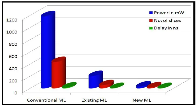
delay measurements are in nano seconds, and area is compared in terms of no: of slices. Table 1 and the fig .14 give the comparisons.
Table 1. Comparison of area, delay and total power.
Table 1 shows the power, area, and delay measurements of conventional, existing and new design of ML detector. The same values are plotted for the bar diagram representation shown in fig. 13, which gives a clear diagrammatic comparison that how much optimization is achieved for the new design of ML detector.
Fig. 13. Bar diagram of comparison of power, area and delay.
VI.CONCLUSION AND FUTURE WORK
VII. ACKNOWLEDGMENT
Our endeavor stands incomplete without dedicating our gratitude to everyone who has contributed a lot towards the successful completion of this research work. We are very much grateful to Mr. Gopalakrishnan, Engineer, KELTRON, Ernakulam, for his constant help and support. And we extend our sincere gratitude to Mr. Prithviraj. A, former Assistant Professor of Electronics and communication department, Nehru College of engineering and research centre, for his support and guidance.
REFERENCES
1. Amirhossein Alimohammad and Saeed Fouladi Fard, “FPGA-Based Bit Error Rate Performance Measurement of Wireless Systems”, IEEE Trans. VLSI systems, Vol. 22, no. 7, pp. 1583-1592, July 2015.
2. Chun-Tao Lin, Member, IEEE, Wen-Rong Wuy, Member, IEEE, and Chia-Yu Liu, “Low Complexity ML Detectors for Generalized Spatial Modulation Systems”, IEEE Trans. Commun., Vol. PP, no. 99, pp. 1-1. 2014.
3. Y. Xiao, Z. Yang, L. Dan, P. Yang, L. Yin, and W. Xiang, .Low complexity signal detection for generalized spatial modulation,. IEEE Commun. Lett., vol. 18, no. 3, pp. 403-406, Mar. 2014.
4. M. M. Mansour, S. P. Alex, and L. M.A. Jalloul, “Reduced complexity soft-output MIMO sphere detectors – part II: architectural optimizations,” IEEE Trans. Signal Process., vol. 62, pp. 5521-5535, Nov. 2014.
5. T.-H. Kim, “Low-complexity sorted QR decomposition for MIMO systems based on pairwise column symmetrization,” IEEE Trans. Wireless Commun., vol. 13, pp. 1388-1396, Mar. 2014.
6. Luis G. Barbero, Member and John S. Thompson,” Fixing the Complexity of the Sphere Decoder for MIMO Detection” IEEE transactions on wireless communications, vol. 7, no. 6, pp.52, june 2008.
7. Yue Xiao, Zongfei Yang, Lilin Dan, Ping Yang, Lu Yin, and Wei Xiang,”Low-Complexity Signal Detection for Generalized Spatial Modulation” IEEE communications letters, vol. 18, no. 3, march 2014.
8. A. Alimohammad, S. F. Fard, and B. F. Cockburn, “Hardware implementation of Nakagami and Weibull variate generators,” IEEE Trans. Very Large Scale Integr. (VLSI) Syst., vol. 20, no. 7, pp. 1276–1284, Jul. 2012.
9. A. Alimohammad, S. F. Fard, and B. F. Cockburn, “Reconfigurable performance measurement system-on-a-chip for baseband wireless algorithm design and verification,” IEEE Wireless Commun., vol. 19, no. 6, pp. 84–91, Dec. 2012.
10. A. Alimohammad, S. F. Fard, and B. F. Cockburn, “An accurate MIMO fading channel simulator using a compact and high-throughput reconfigurable architecture,” IET Commun., vol. 5, no. 6, pp. 844–852, Apr. 2011.
11. B. Holter and G. E. Oien, “On the amount of fading in MIMO diversity systems,” IEEE Trans. Wireless Commun., vol. 4, no. 5, pp. 2498–2507, Sep. 2005.
BIOGRAPHY
Rajasree P R is doing M.Tech in VLSI design, in Nehru College of engineering and research centre. She completed B.Tech in electronics and communication engineering in 2014. Her research interests are wireless communication, low power VLSI design, testing etc.