Dr. Subhashish Bhattacharya).
The thesis focuses from architecture to hardware development of a scalable,
distributed and a flexible Electrical Power System (EPS) for CubeSat, PicoSat and small
satellites. The architecture for the EPS with separate modules for battery charging and
driving the loads highlighting its benefits over the existing EPS has been discussed. EPS
consists of blocks of battery charging modules, Li-Ion batteries, digital controller and point
of load modules to deliver power to the output load. These separate modules make the
complete architecture scalable from 1U to 12U CubeSats for diverse missions and allowing
the EPS to be reconfigurable on the fly which also makes it flexible at the same time. The
design specifications for each of these blocks for the EPS have been discussed along with the
software requirements.
System modeling of the EPS to understand the power flows from the solar panels to
the EPS considering the revolution of the CubeSat in the lower earth orbit and the rotation of
CubeSat at its own axis has been presented. Synchronous buck and synchronous boost
converters are used for designing the battery charging modules and the point of load
modules. Simulation results for synchronous buck and synchronous boost have been
presented. Also, hardware design of each module, protection circuitry and control circuitry is
EPC demo boards. Switching frequencies of 1000 KHz are achieved with the demo board
with 150mA as load current and 15V output voltage. Later a phase leg with gate drive
circuitry for 200V GaN devices is developed and tested. Switching frequencies of 500 KHz
by
Shailesh Ashok Notani
A thesis submitted to the Graduate Faculty of North Carolina State University
in partial fulfillment of the requirements for the degree of
Master of Science
Electrical Engineering
Raleigh, North Carolina
2011
APPROVED BY:
_______________________________ ______________________________
Dr. Subhashish Bhattacharya Dr. William Edmonson
Committee Chair
________________________________ ________________________________
DEDICATION
TOMYPARENTS
GEETANOTANI& ASHOKNOTANI
ANDMYSISTER
BIOGRAPHY
The author, Shailesh Notani was born August 30, 1985 in Kanpur, India. He received his
Bachelor of Technology in Electronics Engineering from National Institute of
Technology-Surat, India in 2007. In 2009 he started pursuing his graduate studies at the Future
Renewable Electric Energy Delivery and Management (FREEDM) Systems Center,
Department of Electrical and Computer Engineering at North Carolina State University. He
is engaged in research in the area of power electronics, small satellite subsystem
development and high switching DC/DC converters.
From 2007 to 2009 he worked as a Design Engineer at Delphi Automotive Systems,
Bangalore India. He has worked on the Engine and Transmission Controller and
Instrumentation Cluster product lines. He also worked as a CM II certified Change Leader
during 2008-2009. In the summers of 2010, he worked as an Intern at United Technologies
Research Center implementing SPI communication between Xilinx FPGA and TI DSP and
designing verilog blocks of PWM generation module in the FPGA. He was also responsible
for hardware for phase leg with 1200V Semikron IGBT with optical gate drive for software
ACKNOWLEDGMENTS
I would like to extend my sincere gratitude to my advisor, Dr. Subhashish
Bhattacharya for his continuous guidance, support and encouragement throughout my
masters program at FREEDM System Center, North Carolina State University. I have gained
a lot of new things both professionally and personally over the last one and half years and
interacted with a lot of bright and diverse people, the learning has been immense. I would
thank Dr. William Edmonson at ASTREC and Dr. Drew Hanser at SRI for providing
valuable feedback on my work. The research work has been supported by Advanced Space
Technologies Research & Engineering Center (ASTREC). ASTREC is an I/UCRC
(Industry/University Cooperative Research Center), a National Science Foundation program
to develop a long-term partnership between academia, industry, and government. I would
thank all the people and partners associated with the center for the support that they have
provided to this research.
I would also thank my friends Arun Kadavelugu, Sumit Dutta, Mihir Shah, Hesam
Mirzaee, Gaurav Bawa and Babak Parkhideh at the FREEDM System Center who have
provided their valuable inputs through lively discussions. I appreciate the help provided by
staff members at the center, especially Karen Autry, Colleen Reid and Hulgize Kassa for the
I would also like to thank my friends Amit Deshmukh, Sushant Sinha, Yajuvendra
Singh Shekhawat, Keshav Rajan, Devanshu Desai for being there for me during my stay at
North Carolina State University and making it a memorable journey.
Finally, I would thank my parents, Geeta Notani and Ashok Notani and my sister
TABLE OF CONTENTS
LIST OF TABLES... ix
LIST OF FIGURES ... x
CHAPTER 1: CubeSat – Subsystems and Electrical Power Subsystem ... 1
1.1 Introduction ...1
1.2 The CubeSat and CubeSat Subsystems...4
1.2.1 Attitude Determination and Control System (ADCS) ... 6
1.2.2 Command and Data Handling (CDH)... 7
1.2.3 High Speed Communications (HSCOM) ... 8
1.2.4 Electrical Power System (EPS)... 8
1.2.5 Structures (STR) ... 8
1.2.6 Payload (PLY) ... 9
1.2.7 Flight Software (FSW)... 9
1.3 The Electrical Power Subsystem...10
1.4 Motivation for EPS Subsystem Design...12
CHAPTER 2: Architecture, Design Specification and System Modeling... 13
2.1 The Clyde-Space EPS...13
2.2 The CubeSat Kit EPS...15
2.3 EPS Architecture...18
2.4 EPS Design Specifications (1U to 12U CubeSats)...20
2.4.1 Solar Panel Specifications... 21
2.4.2 Battery Specifications ... 22
2.4.3 Battery Charging Circuit Specifications ... 22
2.4.4 Point of Load Converter Specifications... 23
2.4.5 Circuit Protection Requirements... 24
2.4.6 Software Requirements... 24
2.4.7 Communication Requirements... 24
2.4.8 Rad-Hard Requirements... 25
CHAPTER 3: System Modeling and Software Design ... 26
3.1 System Modeling...26
3.2 Software Design...32
CHAPTER 4: Hardware Design and Development... 38
4.1 Flexible Battery Charging Module (FBCM) Design...40
4.2 Flexible Digital Point of Load (FDPOL) Design...42
4.3 Path Selection Design and features...43
4.4 Power failure safe recovery design...45
4.5 Current and Voltage measurement Circuitry...45
4.6 MPPT Circuitry Design...47
4.7 Digital Controller...47
4.8 Synchronous Buck and Synchronous Boost Testing results...49
CHAPTER 5: Rad-Hard GaN device testing for CubeSat EPS... 52
5.1 Introduction to EPC GaN devices...52
5.2 GaN Board Phase Leg Testing...54
5.3 Phase Leg Development with GaN Device...58
CHAPTER 6: Discussion and Future Work ... 64
6.1 EPS Architecture...64
6.2 EPS Hardware Prototype...65
6.3 GaN Devices ...65
6.4 Future Work ...66
CHAPTER 7: 3KW, 48V and 24V Buck Converter for Fuel Cells and Solar Powered LED Lamps... 67
7.1 3W LED Rechargeable Lamps...67
LIST OF TABLES
LIST OF FIGURES
CHAPTER 1: CubeSat – Subsystems and Electrical Power Subsystem ... 1
Figure 1.1. ASTRID (1995), a 28kg scientific and technology demonstration micro- satellite ...2
Figure 1.2. O/OREOS (Organism/Organic Exposure to Orbital Stresses), a 5.5 Kg Nano Satellite deployed off of Minotaur IV in 2010...3
Figure 1.3. QuakeSat, a 3U CubeSat launched on June 30, 2003...4
Figure 1.4. Poly Picosatellite Orbital Deployer (P-POD) and its cross section...5
Figure 1.5. The CubeSat Subsystems[9]...7
Figure 1.6. General CubeSat EPS Architecture ...11
CHAPTER 2: Architecture, Design Specification and System Modeling... 13
Figure 2.1 The Clyde-Space EPS System Diagram...14
Figure 2.2 The Clyde-Space EPS Hardware...15
Figure 2.3 The CubeSat Kit EPS System Block Diagram ...16
Figure 2.4 The CubeSat Kit EPS Hardware...17
Figure 2.5 Flexible and Scalable EPS Architecture...18
CHAPTER 3: System Modeling and Software Design ... 26
Figure 3.1 Illumination and Dark period of a CubeSat in LEO...27
Figure 3.2 Output Voltage from one Solar Panel String...27
Figure 3.3 Simulink model of solar panle connections...28
Figure 3.4 Output voltages from six faces of solar panels...29
Figure 3.5 Synchronous Buck converter configured for 3.3V output...30
Figure 3.6 Synchronous Buck converter configured for 5V output...30
Figure 3.7 Synchronous Buck converter configured for 1.8 V output...31
Figure 3.9 Digital Closed Loop control elements [9] ...32
Figure 3.10 FBCM a) power stage b)MPPT/Current Loop c) Voltage Loop Implementation using Digital Controller [9]...33
Figure 3.11 Software Algorithm for Current/MPPT loop [9]...34
Figure 3.12 Dynamic compensator model for battery charging algorithm.[9] ...35
Figure 3.13 FDPOL Control Loop Model [9]...36
Figure 3.14 FDPOL software algorithm [9] ...37
CHAPTER 4: Hardware Design and Development... 38
Figure 4.1 The CubeSat EPS Prototype Developed...38
Figure 4.2 CubeSat EPS Prototype with FDPOL and FBCM indicated...39
Figure 4.3 Flexible Battery Charging Module Schematic ...41
Figure 4.4 Flexible Digital Point of Load – Synchronous Boost Converter...43
Figure 4.5 Flexible Digital Point of Load – Synchronous Buck Converter...43
Figure 4.6 Path Selection switches ...44
Figure 4.7 Power Faliure Circuitry ...45
Figure 4.8 Voltage Measurement Circuitry ...46
Figure 4.9 Current Measurement Circuitry...46
Figure 4.10 Current and Voltage Measurement for MPPT...47
Figure 4.11 DSP Controller card – DIMM package ...48
Figure 4.12 14 Pin JTAG Connector ...48
Figure 4.13 FDPOL 1 Buck Converter – Configured at 5V, 870mA with input VBATT at 7.5V ...50
Figure 4.14 FDPOL 2 Buck Converter – Configured at 3.3V, 570mA with input VBATT at 7.5V ...50
Figure 4.15 FDPOL 3 Boost Converter – Configured at 12V, 710mA with input VBATT at 7.5V ...51
CHAPTER 5: Rad-Hard GaN device testing for CubeSat EPS... 52
Figure 5.1 EPC GaN Power MOSFET Structure...53
Figure 5.2 EPC GaN devices bottom and top view ...53
Figure 5.3 EPC GaN development boards, (a) 100V device, (b) 40V device ...55
Figure 5.4 (a) Rise time measurement of the device. (b) Device switching at 500 KHz ....56
Figure 5.5 Device switching (a) at 600 KHz. (b) at 700 KHz ...56
Figure 5.6 Device switching (a) at 800 KHz. (b) at 900 KHz ...57
Figure 5.7 Device switching (a) at 1000 KHz. (b) at 1100 KHz ...57
Figure 5.8 GaN phase leg board developed with EPC 200V devices...58
Figure 5.9 GaN phase leg board blocks. ...59
Figure 5.10 GaN Buck Converter (250 KHz) with input voltage 50V and output 25V, 101 mA. ...60
Figure 5.11 GaN Buck Converter (250 KHz) with input voltage 60V and output 30V, 117 mA. ...60
Figure 5.12 GaN Buck Converter (250 KHz) with input voltage 80V and output 40V, 153 mA. ...61
Figure 5.13 GaN Buck Converter (250 KHz) with input voltage 100V and output 50V, 186 mA. ...61
Figure 5.14 GaN Buck Converter (500 KHz) with input voltage 60V and output 30V, 117 mA. ...62
Figure 5.15 GaN Buck Converter (500 KHz) with input voltage 100V and output 50V, 238 mA. ...63
CHAPTER 7 ... 67
Figure 7.1 Block Diagram of LaBL Project...68
Figure 7.2 Image for Charging Station and Junction Box ...68
Figure 7.3 Block Diagram for Solar Lantern ...69
Figure 7.4 Fuel Cell Converter Block Diagram...71
Figure 7.6 Bootstrap Gate Driver Circuitry ...73
Figure 7.7 Fuel Cell Converter Board Details ...74
Figure 7.8 48V Converter, 10KHz operation...75
CHAPTER 1
CubeSat – Subsystems and Electrical Power Subsystem
1.1 Introduction
Over the last 20 years there has been a remarkable development in electronics which
has enabled smaller and compact devices that we see around us today. This development has
also enabled building of much smaller satellites with increasing capabilities and more useful
missions which were previously possible with only larger satellites. Consequently new
terminology for these small satellites started to emerge [1]:
x Microsatellites: Satellites less than 100 Kg
x Nanosatellites: Satellites less than 10 Kg
x Picosatellites: Satellites less than 1 Kg
These definitions instead of being strict rather overlap with each other and Nanosatellites and
Picosatellites together are now referred to as Picosatellites. The thesis works deals with the
development of a CubeSat EPS but it serves right to give a broader view of the system we are
dealing with to enhance our understanding.
Figure 1.1 shows the micro satellite ASTRID which was launched on January 24,
1995. It is a 28 Kg technology demonstration satellite to explore neutral particles in orbit for
measuring auroral plasma and for auroral imaging. The cost for launching the satellite was
(O/OREOS) nano-satellite that was launched in 2010 for a 6 month mission. The satellite
conducted space-based biology experiments on how life and the components of life respond
to this complexity. O/OREOS was placed in a low earth orbit at an altitude of 650 Km where
its samples will experience 1/10,000th the gravity on Earth. The size and complexity
reduction in these satellites is remarkable as compared to conventional satellites. This also
results in the reduction of total expenditure incurred for the mission. The smaller satellites
target smaller missions that run from 3 months to a maximum duration of 18 months.
Figure 1.1. ASTRID (1995), a 28kg scientific and technology demonstration micro-satellite
Academic institutes have played a major role in the development of microsatellites
notably from Surrey University in UK and Stanford University from US. In February 2000,
students from Stanford University developed OPAL microsat which successfully deployed
six picosatellites. Based on its success, the collaboration between Prof. Jordi Puig-Suari at
California Polytechnic State University (Cal Poly), San Luis Obispo and Prof. Bob Twiggs at
concept of CubeSat. The prime purpose of CubeSat concept was to develop design standard
for picosatellites with an aim to reduce cost, decrease development time, increase the number
of experimental launches and to increase collaboration between high schools, universities and
private firms focusing on picosatellite development [2].
Figure 1.2. O/OREOS (Organism/Organic Exposure to Orbital Stresses), a 5.5 Kg Nano Satellite deployed off of Minotaur IV in 2010
PicoSatellites are much smaller and target only technology demonstration and student
experiments where proof of concept of smaller modules has to be performed. CubeSats as per
the standard given by Cal Poly, fall in the category of microsatellites. Figure 1.3 shows the
QuakeSat, a 3U CubeSat designed to search for earthquake precursor signals. The satellite
was designed by QuakeFinder, a joint venture between satellite services provider Stellar
Solutions, Lockheed Martin, and the Space System Development Laboratory at Stanford
Figure 1.3. QuakeSat, a 3U CubeSat launched on June 30, 2003
1.2 The CubeSat and CubeSat Subsystems
A CubeSat is a small satellite in the shape of a cube with 10 cm length and a maximum
mass of 1 Kg. It is referred to as 1U. The present standard has modified the weight
requirement for 1U to 1.33 Kg. The CubeSat concept is modular and can be extended to 2U
which is a 10 cm X 10 cm X 20 cm satellite and to 3U which is a 10 cm X 10 cm X 20 cm
satellite. The concept can be extended further and at present people believe that a 12U
CubeSat is also possible. Along with the size requirement the CubeSat standard also requires
other features like a deployment switch, vibration standards, radiation hardness standards,
launch procedures, design requirements etc. These standard size requirements have enabled
the development of launching devices to put these satellites into orbit. This has considerably
which is a housing that can hold upto three 1U CubeSats and release them one by one in
space [4]. Figure 1.4 shows the P-POD developed by Cal Poly. Any CubeSats being
developed have to be reported to Cal Poly and should adhere to the latest CubeSat standard.
The present cost of launch of CubeSat is around US $40,000 and present development time
for a CubeSat is around 2 years. With professional partners the development time would
reduce considerably.
Figure 1.4. Poly Picosatellite Orbital Deployer (P-POD) and its cross section
A satellite development involves extreme design restrictions that limit the choices of
components: Size, weight, power consumption, and ruggedness are of paramount concern.
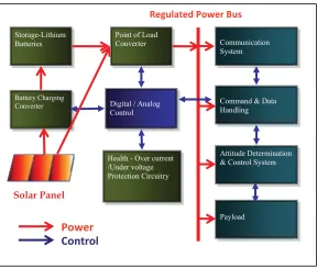
Figure 1.5 below gives a general idea of the subsystems typically present on a CubeSat. The
1.2.1 Attitude Determination and Control System (ADCS)
The Attitude Determination and Control System (ADCS) is responsible for keeping
the satellite in the projected orbit. The ADCS passively points the high speed
communications antenna in the ideal orientation to achieve the highest quality link. The
ADCS system consists of three main components: a permanent magnet, hysteresis rods, and a
magnetometer. The attitude control is made up of one magnet that is primarily used for
satellite stabilization about the magnetic field. This magnet aligns lengthwise with Earth's
magnetic field, providing one axes of stabilization. The third axis is not stabilized and the
satellite will spin freely about the longitudinal axis of the magnets. Three magnetic hysteresis
rods are used for magnetic damping to prevent oscillation about the spin axis. The control
system provides the correct positioning of the spacecraft during communications with the
ground station. The magnetometer is used to determine the satellite’s position and
orientation. It takes readings and sends them to Control and Data Handling (CDH), where the
Figure 1.5. The CubeSat Subsystems[9]
1.2.2 Command and Data Handling (CDH)
The Command and Data Handling (CDH) system is responsible for coordinating data
communication between systems and to the ground station, as well as regulating
autonomously the state of the CubeSat. The CDH system relies on the operation of all other
subsystems to succeed and communicates with electrical subsystems over a variety of buses.
The CDH in most of the application is capable of reprogramming both itself and the primary
communications system. The interactions between the different subsystems are limited to the
maintaining their state of health and communicating to the CDH for the complete assessment
of the satellite. Some communication between the subsystem regarding the operational
1.2.3 High Speed Communications (HSCOM)
The Primary Communication (PCOM) system is responsible for providing the data
link between the Command and Data Handling (CDH) system and the ground station to
communicate control commands as well as receive health and status data through a
bidirectional, full duplex communication system. The PCOM system is made up of three
main components: the antenna design, the terminal node controller (TNC), and the
radio/transceiver.
1.2.4 Electrical Power System (EPS)
The Electric Power System (EPS) primary mission is to process and distribute
electrical energy to operate the various systems in the CubeSat. The EPS takes in power from
strings of solar panels and stores in Li based batteries. The solar panels and the Li based
batteries are a part of the EPS subsystem. Energy stored in the batteries is then used to power
up the different subsystems of the CubeSat. The next section discusses the EPS in detail.
1.2.5 Structures (STR)
The CubeSat structure includes all necessary mounts and support structure, such that
the other subsystems are safely housed. The external structure provides the only protection
from the space environment, and provides critical radiation shielding to sensitive
components. It also provides the mechanical and electrical interface to the P-POD deployer.
the bottom of each rail propel the satellite out of the P-POD. As per the CubeSat requirement
the satellite is activated when the separation switches on the rails lose contact with the
P-POD rear plate.
1.2.6 Payload (PLY)
The payload for CubeSat are generally proof of concept experiments or small
isolated task or a distributed task. With the limited space of the CubeSat, designing a payload
which does some meaningful application is becoming more challenging and threatening to
the development of the CubeSat concept. Never the less, Payload is an inportant subsystem
and generates a lot of different requirement in terms of power for the EPS and size and
weight for the structure.
1.2.7 Flight Software (FSW)
The flight software is another critical subsystem. It is the brain inside all the
subsystems. An efficient software flow is essential for a successful operation. The software
includes different modes of operation. In particular the thesis concentrates on the software
related to the EPS, the algorithm for maximum power point tracking, battery charging and
scheduling the point of load converters. This has been discussed in detail in the later
chapters.
The intra subsystem communication is also essential for proper data flow and state of
1.3 The Electrical Power Subsystem
The EPS is one of the most important subsystem from engineering point of view as it
manages the power available for the satellite for use and its efficiency it directly related to
the efficiency of the satellite. The size, weight and scalability requirements for the CubeSat
make it more challenging to design a versatile EPS for the CubeSats [6]. The EPS interfaces
with the solar panels and the Li based batteries which act as storage. It runs MPPT
algorithms, battery charging algorithms, state of charge determination algorithm. Also it
generates the supply voltages needed by the subsystems in the CubeSat.
Figure 1.6. General CubeSat EPS Architecture
Some common issues that we can point out with this general architecture and which decrease
the efficiency of the EPS are listed below.
1 The different subsystems have different converters inside them which reduce efficiency
because of double conversion.
2 Some subsystem can run more efficiently at lower voltages or at a specified voltage.
3 There are different varieties of payloads that can be attached to the CubeSat and would
require different power supply or an inbuilt power supply.
There are at present three providers of CubeSat EPS, the first and the most preferred
being Clyde space and the second being CubeSat kit and the third being Pumpkin kit. All
Solar Panel Storage-Lithium
Batteries Communication
System
Battery Charging Converter
Point of Load Converter
Command & Data Handling
Attitude Determination & Control System
Payload Digital / Analog
Control
RegulatedPowerBus
Health - Over current /Under voltage Protection Circuitry
three have their merits and demerits. We would discuss these architectures in the next chapter
and compare them with out architecture for the EPS.
1.4 Motivation for EPS Subsystem Design
CubeSat design itself presents a challenge in terms of the size, weight, multiple tasks
and the harsh environment constraints it has, the EPS subsystem is one of the least bothered
about component in the CubeSat which is still in the initial development stages in different
universities. But we realize that EPS is a very important subsystem of the CubeSat and a lot
of contribution can be made in this regard. To put the facts, at present there are only two
vendors which provide the EPS for the CubeSats, namely Clyde-Space and CubeSat Kit. The
room to contribute and to address multiple issues at the same time led us to the development
of the EPS. The major motivations behind the EPS subsystem design are as follows:
1) Absence of a flexible, scalable and a reconfigurable EPS subsystem that would meet
the most diverse mission requirements and at the same time is efficient.
2) Absence of an EPS which gives the user the option to use Li-Ion battery models and
control the state of the EPS
3) Absence of an EPS which has user programmable multiple output voltage lines to
eliminate the need of an additional converter present in the other subsystem.
4) Absence of a single EPS which is low cost and at the same time can be used in 1U to
CHAPTER 2
Architecture, Design Specification and System Modeling
In this chapter we discuss the present architecture of the present EPS provides, namely
Clyde-Space, CubeSat Kit and Pumpkin Kit. We would go though their EPS block diagrams
and investigate their merits and demerits. Going forward we compare the CubeSat
architecture developed and discuss in detail the features in the EPS. We would then go
though the specifications for the hardware and software design for the EPS.
2.1 The Clyde-Space EPS
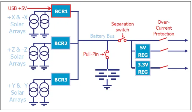
Figure 2.1 shows the architecture of the Clyde-Space EPS [7]. The EPS consists of 3
Battery Charging circuits (BCR) of different power ratings. The MPPT algorithm runs in
these BCR’s to extract maximum power from the solar panels. The BCR tracks the MPP of
the array as long as it is above 3.6V and below 25V. Implementing MPPT for individual
faces gives the maximum system efficiency. The EPS connects the panels on the opposite
faces in parallel as it forms the best case for using less number of BCR and at the same time
maintaining higher efficiency for the system. The Energy processed is passed on to the
Figure 2.1 The Clyde-Space EPS System Diagram
The output of the EPS is a 5V regulated line, 3V regulated line and an unregulated
line. The figure 2.2 shows the Clyde-Space EPS hardware showing the PC104 connecter. The
three BCR modules are also visible along with the 5V and 3.3V regulators. The EPS also
includes different protection features which include limited the output current from the 5V
and 3.3V regulated lines. Battery under voltage/ over voltage protection feature is also
included in the EPS. The batteries are not included as a part of the EPS but treated as an
additional board. The main drawback of the architecture presented is the two DC bus
voltages at the output side. These voltages are not reconfigurable to any other voltage level.
Due to this reason it results in a separate voltage regulator inside the other subsystems which
do not run on 3.3V or 5V. Also, it does not give the user a complete control of the CubeSat
in a CubeSat. Also, there is no flexibility available to the user in terms of the control
algorithms to be implemented.
Figure 2.2 The Clyde-Space EPS Hardware
2.2 The CubeSat Kit EPS
The figure 2.3 shows the system block diagram for the CubeSat kit EPS [8]. This
design also provides 5V and 3.3V regulated outputs but instead of using switching regulators,
linear regulators are being used. This has its own benefit of being less noisy but on the other
hand the user has to compromise on the system efficiency. Two Li-Ion batteries are made
part of the EPS. The CubeSat Kit provides two Iphone batteries along with the EPS. There is
dedicated battery charging circuits for each battery. The battery chargers do not implement
microcontroller and implements the protection circuits as a part of the control algorithm. The
presence of a programmable digital controller gives it the needed flexibility and the control to
the user. The EPS does not implement a MPPT control to in the battery charging circuit.
Figure 2.3 The CubeSat Kit EPS System Block Diagram
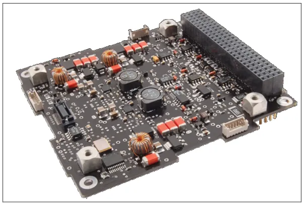
The figure 2.4 shows the hardware for the CubeSat Kit EPS. The battery is mounted
over the board. PC 104 Connector is placed as per the standard. Power disconnect relays are
also present instead of MOSFETS. Over current protection is implemented on both of the
regulators are started again. The EPS also supports I2C communication with the other
subsystems. The weight of the EPS with the batteries is 155 grams and is meant for only 1U
to 3U and source upto 1A on the 5V line, 500mA on the 3.3V line and 1.5A on the
unregulated battery voltage line. The EPS is designed with automotive grade components.
The batteries can be configured and connected in series or in parallel with a limitation on
maximum battery input voltage being less than 10V. The complete design is implemented on
a two layer PCB. The EPS also provides a USB port for battery charging with charging
current limited to 500 mA.
2.3 EPS Architecture
Figure 2.5 below shows the CubeSat EPS architecture developed along with ASTREC.
After considering the advantages and disadvantages of the two EPS discussed above the need
for a modular and scalable architecture for the power supply system which can be used for
any number of subsystem voltages and any payload voltage requirement is highlighted. It
inherits the system goals for the general CubeSat EPS architecture and yet can be scaled from
1U to 12U [9].
Figure 2.5 Flexible and Scalable EPS Architecture
The architecture has three Flexible Battery Charging Modules (FBCM) which can
interface with three different solar panel strings. FBCM forms the critical interface between
the solar panels and the energy storage device. The FBCM directs all the energy to the
Synchronous Buck Converters Point of Load Synchronous Buck
Converters Point of Load
Wide Input Synchronous Buck-Boost Charger (FBCM) Solar Panels PV Wide Input Synchronous Buck-Boost Charger (FBCM) Solar Panels PV Wide Input Synchronous Buck-Boost Charger (FBCM) Solar Panels PV Synchronous Buck Converters Point of Load (FDPOL)
Synchronous Buck Converters Point of Load (FDPOL) Path Selection Switch closes Sun Time Plug-n-play Chargers Multiphase 12V Synchronous Boost Converters
Point of Load (FDPOL) 5V 3.3V F280x Digital Controller P W M C O M M S A D C I O Synchronous Boost Converters
Point of Load (FDPOL)
storage cells, which are made flexible and for a wide range of voltages or number of
batteries. The number of solar cells used in the small satellites usually varies with different
missions and the type of payloads used. The prototype has a provision of interfacing with two
strings of energy storage devices either Li based batteries or ultra-capacitors. The
unregulated DC bus voltage from the battery and as well as the solar panel to a regulated DC
voltages for the different payloads and subsystems is generated by Flexible Digital Point of
Load (FDPOL) modules. As the name suggests, these modules are made with the flexibility
of changing the point of load voltages since they are digitally controlled. The most common
voltages of 3.3V, 5V, 12V, 15V being used can be easily generated with either the
synchronous buck or synchronous boost converters. Since they are powered from both solar
panel and the battery, the FDPOL modules are made suitable for higher system line voltage
variation range.
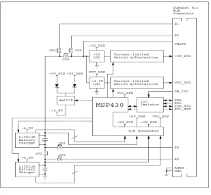
The EPS core is a digital controller which interfaces with the battery charging module
namely FBCM, the FDPOL modules, the State of Health (SOH) module and fault protection
and diagnostic circuitry. The prototypes central digital power controller is TI
TMS320F28335 DSP which takes the feedback and gives out control signals. The central
digital power controller controls the power stage and also makes the power system flexible.
The FBCM is user programmable using the Flexi-sat Digital Power Designer Software. The
user can configure the FBCM with the required output voltage (battery voltage), operating
frequency, charging current and adjust loop compensation parameters. The FDPOL operation
program the regulated voltage, current and switching frequency, independent modules and
which modules are paralleled. In the sections below we describe the different specifications/
requirements for the EPS and discuss how the hardware was designed to meet those
requirements.
2.4 EPS Design Specifications (1U to 12U CubeSats)
Design requirement gathering are the toughest part of any design. CubeSats are still
limited to educational institutes and all the subsystems are custom made. There are only two
vendors for the EPS at present. With rapid innovation on Solar Panel mechanical design and
many deployable solar panels being developed, new CubeSat sybsystems being developed
and new proof of concept experiments being developed requiring diverse payloads, it
becomes very critical to be able to design a scalable, flexible and reconfigurable EPS which
would meet the requirements for a large number of CubeSat missions. The following chapter
discusses the EPS design specification for the various blocks presented in the architecture
above, the Li based batteries and the Solar Panels.
Not all the requirements listed below have been targeted for in the EPS prototype.
The primary goal of the EPS is to aid faster development for subsequent EPS and to serve as
TABLE I. SOLARPANELCONFIGURATION AND POWER SPECIFICATIONS
Side Solar Panel (4) Top & Bottom Panel (2)
Power Vmp Imp Power Vmp Imp
Config. Total Power (W)
(W) (V) (mA) (W) (V) (mA)
1U 12.27 2.05 4.7 435 2.05 4.7 435
2U 20.45 4.09 4.7 870 2.05 4.7 435
3U 28.62 6.13 14.1 435 2.05 4.7 435
4U-a 36.80 8.18 18.8 435 2.05 4.7 435
4U-b 32.71 4.09 9.4 435 8.18 18.8 435
5U 44.98 10.23 4.7 2175 2.05 4.7 435
6U-a 44.86 9.17 14.1 650 4.09 4.7 870
6U-b 53.16 12.27 14.1 870 2.05 4.7 435
8U-a 69.54 16.36 9.4 1740 2.05 4.7 435
8U-b 57.42 12.31 9.4 1310 4.09 9.4 435
10U 69.30 15.28 23.5 650 4.09 9.4 435
12U-a 81.78 18.40 14.1 1310 4.09 9.4 435
12U-b 77.70 16.36 18.8 87 0 6.13 14.1 435
2.4.1 Solar Panel Specifications
Spectrolab, Emcore, Clyde Space and Azurspace are the four major suppliers of
CubeSat solar panels. Depending upon the voltage and capacity of battery being used and the
type of CubeSat, i.e., 1U, 3U or 12U different configurations for the solar panels can be
designed. The user has an option of selecting any supplier for the solar panels and also any
configuration to connect these solar panels. The solar panel connections depend mainly on
the battery that has been chosen for the mission which in return is dependent on the
subsystems and the payload being used in the satellite. Thus it is important to understand
what the input to the EPS is going to be depending on the different solar panels and different
CubeSat configurations. The table below gives the chart of various configurations for the
possible but at the end would result in same voltage and power levels. The above table is
based on the Spectrolab’s 28.3% efficient ultra triple junction (UJT) solar cells.
2.4.2 Battery Specifications
Li based batteries are used in CubeSats owing to their compact size and light weight.
Depending upon the CubeSat configuration a battery of 3.7V, 7.4V, 14V, 20V or 30V can be
chosen. The subsystems being used in the CubeSat and the Payload for which the satellite is
being designed for play a major role in battery voltage and capacity selection. Also most of
the subsystem are not always ON and follow the wake/ operate/ sleep mode of operation. The
EPS designed should be capable of interfacing with a battery voltage of 3V to 30V. There are
generally two batteries used in the CubeSat the second battery being used as a back up
resource. The hardware should be capable of charging these batteries individually and
selecting which battery to be used to drive the loads.
2.4.3 Battery Charging Circuit Specifications
The specification of the FBCM depend on mostly the input that is the solar panel
specification and secondly the battery which is the output for the battery charging circuitry.
FBCM should be able to operate to a maximum input voltage of 30V. It should have an
undervoltage shut down protection that is programmable. This voltage depends on the battery
voltage. Secondly, FBCM should be able to interface with the Li based batteries which can
have a maximum voltage of 30V.
There are three FBCM modules being proposed in the architecture. They should be
able to paralleled together and charge the battery. Also it should implement protection
against over charging. In case the battery is completely charged and more energy is available
from the solar panels, it should be diverted to the loads directly. It should follow procedures
involved in Li-ion battery charging.
2.4.4 Point of Load Converter Specifications
The point of load converters should be driven through the Battery power or from the
power delivered through the solar panels. Multiple modules of point of load converters
should be present. All the system voltages from 1.8V to 50V should be generated from these
point of load modules. This breaks down to implementing synchronous buck and
synchronous boost topologies for output voltages smaller than the battery voltage and output
voltages greater than the battery voltage respectively. The output current of these point of
load modules should be limited to a maximum of 2A and the converter output voltage should
not drop incase 2A limit is reached. An internal flag has to be raised when such a condition
arises and if the fault is not removed the load should be cut off from the supply. These point
of load modules should be configurable on the fly and can be turned completely off when
2.4.5 Circuit Protection Requirements
Protection of the CubeSat EPS and the subsystem is essential and all diagnostic
routines should be implemented. Short circuit and open circuit faults at all input and output
connectors should be monitored and logged in the controller. Periodic attempts to a
maximum of three should be made in case a fault is detected to determine if its an
intermittent fault or a permanent fault. Current and voltage measurements should be done at
the input and output connectors. Battery voltage and current should be monitored and over
current and short circuit protection should be implemented.
2.4.6 Software Requirements
A scheduler has to be designed and all the converters in the FBCM and FDPOL
modules are to be implemented as tasks. The user should be able to call these tasks
individually and configure the complete system and implement its own running algorithm.
The software should also take care of MPPT algorithm [10], battery charging algorithm,
controls for the converter and data logging. The software is responsible to generate a
complete state of health report and update it periodically.
2.4.7 Communication Requirements
All the data logged and state of health indicators should be communicated to the other
subsystem in the CubeSat over the I2C bus. The baud rate and data messages should be
2.4.8 Rad-Hard Requirements
The EPS should comply with the Rad-Hard space requirements listed below [11], the
aim is to minimize the amount of aluminum required for shielding and make savings on the
weight required for the shielding of the CubeSat.
TABLE II. STANDARD RADIATION CATEGORIES FOR HARDWARE
Category Total Ionising Dose T.I.D. (kRad)
Single Event Latch-Up S.E.L. (MeV)
Single Event Upset S.E.E. (MeV)
Rad hard 100 minimum Up to 120 Up to 120
Rad
Tolerant 100 maximum Up to 120 Up to 120
Commercial 3-20 1-120 1-120
2.4.9 Mass and Size Requirements
The mass of the EPS along with the batteries should be 200 grams at the max [7] [8].
The EPS board has to fit in a Cube of 10 cms. The dimensions of the board should 95 mm x
CHAPTER 3
System Modeling and Software Design
In order to design the software for the EPS and the battery integration with the EPS, it
is necessary to model the EPS in parts. Apart from the software design the system modeling
also helps us understanding the different conditions for which the design is intended. Starting
from the input to the EPS, that is modeling the solar panels and the revolution of CubeSat
around the earth to the point of load converters which deliver to the output load modeling
gives us an understanding of system and aids software development taking in account various
conditions.
3.1 System Modeling
The CubeSats are placed in low earth orbit [12] at an altitude of 500 KM to 1500 KM
and take about 90 minutes for one revolution around the earth. In the 90 minute duration it
faces the sun for 50 minutes and for the rest 40 minutes it is in the earth shadow area. Figure
3.1 below shows the revolution of CubeSat around the Earth at a speed of 16.68 m/s. The
CubeSat thus can harness power in this 50 minute duration and it relies on the battery power
for the 40 minute duration or is kept in the sleep mode for this duration. Figure 3.2 shows the
ideal voltage output of one string of solar panels (opposite face of solar panel connected in
well. In that case the total power coming into the CubeSat has to be considered. In figure 3.3,
the CubeSat is rotating at 20 rmp
Figure 3.1 Illumination and Dark period of a CubeSat in LEO
Figure 3.3 shows the CubeSat solar panels on each of the six faces. Also the CubeSat is
rotating on its own axis at 20 rpm. To make it more realistic the CubeSat is inclined at an
angle of 30 degrees with the solar rays coming. Thus each solar panel never receives more
than 70% illumination. The paralleling of these faces is done in the EPS in order to reduce
the number of FBCM.
Figure 3.3 Simulink model of solar panle connections
Figure 3.4 shows the ideal output voltages of three solar panel strings considering solar
panels on each phase to be of equal power rating. The CubeSat is rotating on its diagonal axis
at 20 rpm. We see the output voltages of opposite faces are opposite in phase as well which
justifies our thinking behind connecting them in parallel.
1 Vout1 1 rotation Wrap To Zero5 Wrap To Zero4 Wrap To Zero3 Wrap To Zero2 Wrap To Zero1 Wrap To Zero Sine Wave Function 5 Sine Wave Function 4 Sine Wave Function 3 Sine Wave Function 2 Sine Wave Function 1 Sine Wave Functio n Product5 Product4 Product3 Product2 Product1 Product Ip v Insolatio n Vpv Ppv
PV module (I)
PV6 Ip v Insolatio n Vpv Ppv
PV module (I)
PV5 Ip v Insolatio n Vpv Ppv
PV module (I)
PV4 Ip v Insolatio n Vpv Ppv
PV module (I)
PV3
Ipv Insolation
Vpv Ppv
PV module (I)
PV2
Ipv Insolation
Vpv Ppv
PV module (I)
PV1
PV Panel 6 Voltage PV Panel 6 Power
PV Panel 5 Voltage PV Panel 5 Power
PV Panel 4 Voltage PV Panel 4 Power
PV Panel 3 Voltage PV Panel 3 Power
PV Panel 2 Voltage PV Panel 2 Power
PV Panel 1 Voltage1 PV Panel 1 Voltage
PV Panel 1 Power
max MinMa x 1000 Insolation6 1000 Insolation4 1000 Insolation3 1000 Insolation2 1000 Insolation1 1000 Insolation 1 I max
Figure 3.4 Output voltages from six faces of solar panels
FBCM is a synchronous buck converter followed by a synchronous boost converter. At
any given time only one of the converters would be working and the other would act like a
closed switch to pass on the current through it. The modeling of the synchronous buck and
synchronous boost is presented in the previous work on CubeSat [9]. Average ac modeling in
continuous conduction mode, open loop transfer functions in CCM and DCM modeling have
been completed previously along with compensation and closed loop gain plots [9]. The
output of the FBCM module being the Li-Ion battery battery impedance curves were derived
and the control to output voltage transfer functions were derived to be readily used. FBCM
modules are capable of implementing MPPT algorithm. Adaptive P&O method developed as
part of previous work has been tested and is well suited for CubeSat application due to
FDPOL modules are again synchronous buck and synchronous boost converters [14]
and there functions derived are on similar lines as on FBCM. Figure 3.5 to figure 3.8 show
the Synchronous bcuk and synchronous boost plots for the EPS.
Figure 3.5 Synchronous Buck converter configured for 3.3V output
Figure 3.7 Synchronous Buck converter configured for 1.8 V output
3.2 Software Design
The software design consists of two things, the first being the software architecture and
secondly its implementation. The standard software architecture to design a scheduler and
implement all the functions as tasks is optimum for CubeSat. Writing the control loops for
the synchronous buck and synchronous boost converters and implementing MPPT algorithm
in the FBCM. Details of implementation of digital control and algorithms for control (FBCM
control loop and FDPOL control loops) have been given in the previous work [9] [15] and
have not been discussed here.
Kpwm
Gdelay K2p2z
Vref Gplant Gdiv Voutput Sense ADC Keadc Controller Delay PWM + -Power Stage Duty G(s) H(s) DSP Engine Voltage Sense
Figure 3.9 Digital Closed Loop control elements [9]
Figure 3.9 shows the closed loop block diagram to implement the digital control of a
DC/DC converter. It senses the feedback voltage and compares it with a digital reference
control like TMS320F28335 to control a converter. Figure 3.10 shows the FBCM control
loop. Figure 3.10 (a) shows the power stage of the FBCM, (b) shows the MPPT control/
current loop and (c) shows the voltage control loop which is implemented in a digital
controller. Gate Signal PV Voltage PV Current Lo Co Ci To Battery Gate Signal Battery Current Battery Voltage PV (a) PV Current PV Voltage 1 MHz Current Controller CNTL 2P2Z Uout Ref FB A D C H W rslt1 ADC DRV DutyCmd E P W M H W Duty BUCK-BOOST DRV 300 KHz MPPT Uout V I rslt0 Gate Signal ICmd Ind Current rslt2 A D C H W rslt0 ADC DRV DutyCmd E P W M H W Duty BUCK-BOOST DRV 300 KHz CNTL 2P2Z Uout Ref FB Voltage Controller V bat Battery Voltage Gate Signal (c)
Figure 3.11 shows the software algorithm for the MPPT. When the battery is not charged
the Current loop charges the battery with constant current. After the battery is fully charged
the voltage mode takes over.
Current Controller CNTL 2P2Z Uout Ref FB CNTL 2P2Z Uout Ref FB Voltage Controller
Real Zeros Complex Zeros
Dynamic Current mode Voltage Mode DYNAMIC COMPENSATOR
b2_r, b1_r,b0_r b2_c, b1_c,b0_c
Figure 3.12 Dynamic compensator model for battery charging algorithm.[9]
A dynamic compensator is also designed in the previous work for battery charging
algorithm. Figure 3.12 shows the dynamic compensator. Figure 3.13 shows the FDPOL
control loop. The FDPOL control loop is just one voltage control loop. As a part of the
previous work stability models for the charging control loop and voltage control loop were
developed and it was concluded that a single compensator may not yield an optimum closed
loop control. Taking the example of the buck boost power stage compensation, the charging
control loop is rather simple to stabilize due to the two poles in the system are spread out. For
stabilizing the system we can use two real zeros and an integrator pole to adjust the gain and
to get the desired crossover frequency. When the charging loop is discontinued and the
voltage loop has begun, the power stage transfer function has a double pole. The digital
controller platform allows us to adjust the FIR coefficients of the compensator to get a pair of
Figure 3.13 FDPOL Control Loop Model [9]
A Flexi-sat Digital Power Designer Software was developed to help the user program
the controller according to the power stage to get the desired stability and output voltage.
Figure 3.14 shows the FDPOL software control algorithm to be implemented in the DSP. As
mentioned above it is just on voltage loop. The controller timer, ADC and PWM peripherals
are used in the control algorithm. The control algorithm is implemented in an ISR which
Start
Initialise ADC,PWM Modules
Initialise Time Bases and Drivers
Call ISR
Background Loop PWM Interrupt
Compare with Vref
2 Pole 2 Zero Compensation b0_v,b1_v,b2_v Do conversion,
BatteryVoltage
Return PWM Interrupt
Update PWM Voltage Loop
CHAPTER 4
Hardware Design and Development
In the previous chapter we discussed about the CubeSat EPS architecture and the
different blocks in detail. We also discussed the specifications for each of these blocks. This
chapter deals with the hardware design for each of these blocks and the different features that
the hardware is capable of supporting. Parametric calculations and extreme value analysis
was performed for circuit design.
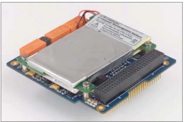
Figure 4.1 The CubeSat EPS Prototype Developed
The figure 4.1 shows the hardware prototype developed for the EPS. The layout was
DSP for development and need based selection. Total number of components in the
schematic is 377 and parts have been optimized to keep the part count low. The total number
of parts being used is 35. This helps in keeping the cost for the prototype board low. The
figure 4.2 shows the different EPS blocks labeled and the approximate area they occupy.
There are two input connectors which are used to interface with the Solar Panels. The output
connector is for the point of load converter outputs. A connector for connecting two batteries
is also provided. One connector for I2C communication is also provided.
Figure 4.2 CubeSat EPS Prototype with FDPOL and FBCM indicated
FBCM – 1 Buck Boost Converter
FBCM – 2 Buck Boost Converter
4.1 Flexible Battery Charging Module (FBCM) Design
The input voltage from the solar panels can vary a lot, thus a wide input converter is
required to interface with the solar panels. From the specification from the previous chapter
the input voltage coming in to the EPS can vary from 0V to 30V depending on the solar
panel configuration and the amount of illumination on the panels. The amount of current
coming in the EPS also depends on the series and parallel connections for the panels. The
maximum current coming into the EPS can be at the maximum 2A. Also this converter has to
interface with the battery whose voltage can be 30V in some of the CubeSat missions. We
selected buck followed by boost topology for the converter. The converter works in the buck
mode when the input voltage is higher than the battery voltage and in the boost mode when
the input voltage from the solar panels is lesser than the battery voltage. The EPS has three of
these battery charging circuits and connect to two arrays of solar panels. The solar panel
arrays on the opposite faces of the EPS are connected in parallel through diodes to the EPS.
Figure 4.3 Flexible Battery Charging Module Schematic
The Mosfets are rated for a breakdown voltage of 60V. The MOSFET Q1 and Q2
with the inductor L2 for the Buck converter part of the FBCM. The input voltage coming
from the solar panel and the input current is monitored by the controller. Similarly the
inductor current and the output voltage is also monitored and used in the control algorithm.
Induction L1 is a ferrite bead used to reduce the input noise. Capacitor C1 and C8 are used
for ESD protection. Resistor R1 is the current sensing resistor and voltage across it is
amplified and sent to the controller. The three FBCM modules can be paralleled together to
increase the amount of current to charge the battery and to supply to the loads. Using this
FBCM block approach gives the scalability required for the EPS. Additional FBCM
4.2 Flexible Digital Point of Load (FDPOL) Design
The FDPOL convert the unregulated battery voltage to regulated voltages to be used by
the different subsystems of the CubeSat. The battery voltage can be a maximum of 30V for
the present design. The hardware has four point of load converters, two of them being
synchronous buck converters for output voltages less than the unregulated battery voltage
and the remaining two being synchronous boost converter for output voltages greater than the
battery voltage. Each of the point of load converter can give an output current of maximum
3A. The LC filter is designed for 5% output voltage ripple. Typically, the small satellite
subsystems being developed by different vendors would work more efficiently at different
input voltages. The synchronous buck and synchronous boost topology is very efficient and
compact. These can be reconfigured to provide a wide range of output voltages including the
standard 1.8V, 3.3V, 5V, 9V, 12V, 15V and 3A of current at each module. Figure 4.4 and
figure 4.5 provide the schematic for the synchronous boost and synchronous buck converter.
The devices with a breakdown voltage of 60V have been selected. The battery voltage which
is the input to the converters, the output voltage of these converters and the inductor current
Figure 4.4 Flexible Digital Point of Load – Synchronous Boost Converter
Figure 4.5 Flexible Digital Point of Load – Synchronous Buck Converter
4.3 Path Selection Design and features
The point of load converters can be fed directly from the battery while the power from
panel directly to the point of load converters and bypassing the battery. The third but a rare
option can be keeping both the switches on so that power available form the solar panels is
directly fed to the point of load converters and the remaining power can be used to charge the
battery and in case the load requirement is higher both the battery and the solar power can be
fed to the FDPOL. The figure 4.6 shows the power path selection features with PMOS being
used as switches to direct the power as required by the algorithms.
4.4 Power failure safe recovery design
In case of complete power loss of battery power, considering the worst case, the circuit
shown in the figure 4.7 comes in picture. The input from the controller keeps the circuit in
off state. In case of loss of this signal due to complete loss of battery power, the circuit
switches ON and charges the battery automatically. When the battery is sufficiently charged
the normal operation takes over. The controller switches on the MPPT algorithm and charges
the battery and drives the load.
Figure 4.7 Power Faliure Circuitry
4.5 Current and Voltage measurement Circuitry
The voltages of various nodes are monitored in the EPS. These voltages are fed to the
ADC of the controller through a resistor divider and a RC filer. The controller has a 10bit/ 12
FBCM and the output voltages of the FDPOL are monitored in this manner. Figure 4.8 shows
the typical voltage divider circuitry with the RC filter. Also the input current, the inductor
current through the FBCM, the inductor current through the FDPOL are monitored. A series
resistor of 25 mOhm is used and the voltage drop across the resistor is amplified with an
Op-amp and fed to the ADC channel of the controller. Figure 4.9 shows the operational Op-amplifier
circuitry.
Figure 4.8 Voltage Measurement Circuitry
4.6 MPPT Circuitry Design
Form the hardware point of view this circuitry is mainly related to monitoring the
current which is drawn from the Solar Panels into the battery charging circuitry and
monitoring the voltage of the solar panels at the MPPT sampling interval [10]. The algorithm
for the MPPT would require these values. The figure 4.10 shows the circuitry used for
monitoring the current and the voltages.
Figure 4.10 Current and Voltage Measurement for MPPT
4.7 Digital Controller
The digital controller is used to give the flexibility required for the EPS. Digital
customize the software for their CubeSat mission. The hardware designed is compatible with
the following TI DSP:
a) TMS320F28335 (floating point CPU)
b) TMS320F2808 (fixed point CUP)
c) TMS320F28044 (fixed point CUP)
The controller cards available for these DSP in the 100 pin DIMM (Dual in Line
“Memory Module”) style vertical pulgin packages that would directly do in the EPS. A 14
PIN JTAG port (Figure 4.12) is also given in the prototype board which is used to directly
program and debug during software development on the hardware. Figure 4.11 shows the
100 pin DIMM style controller card.
Figure 4.11 DSP Controller card – DIMM package
4.8 Synchronous Buck and Synchronous Boost Testing results
Both the FBCM and FDPOL are synchronous buck and synchronous boost converters.
The test results for testing with DC power supply have been presented here. The DC source
voltage was kept at 7.5 V and the four point of load converters were configured to run at
different voltages. The design has two synchronous point of load converters. Figure 4.13
shows FDPOL synchronous buck converter operating at 150 KHz with an output voltage of
5V. The output load current is 870 mA.
Figure 4.14 shows FDPOL synchronous buck converter operating at 150 KHz with an
output voltage of 3.3V. The output load current is 570 mA. The input voltage is the same DC
source kept at 7.5V in place of a 7.5 V battery. The two synchronous boost converters were
configured to work on 12 V and 15 V respectively. Figure 4.15 shows FDPOL synchronous
boost converter operating at 150 KHz with an output voltage of 12V. The output load current
is 710 mA.
Figure 4.16 shows FDPOL synchronous boost converter operating at 150 KHz with
an output voltage of 15 V. The output load current is 890 mA. The input voltage is the same
Figure 4.13 FDPOL 1 Buck Converter – Configured at 5V, 870mA with input VBATT at 7.5V (Chanel 2&3 – PWM pulse A&B at 150 KHz, Chanel 1 – output current and Chanel 4 – Output Voltage. Time Scale: 2
us/ Division)
Figure 4.14 FDPOL 2 Buck Converter – Configured at 3.3V, 570mA with input VBATT at 7.5V (Chanel 2&3 – PWM pulse A&B at 150 KHz, Chanel 1 – output current and Chanel 4 – Output Voltage. Time Scale: 2 us/ Division)
Output Voltage
Output Current
PWM Pulse A/B
Output Voltage
Output Current
Figure 4.15 FDPOL 3 Boost Converter – Configured at 12V, 710mA with input VBATT at 7.5V (Chanel 2&3 – PWM pulse A&B at 150 KHz, Chanel 1 – output current and Chanel 4 – Output Voltage. Time Scale: 2 us/ Division)
Figure 4.16 FDPOL 4 Boost Converter – Configured at 15V, 890mA with input VBATT at 7.5V (Chanel 2&3 – PWM pulse A&B at 150 KHz, Chanel 1 – output current and Chanel 4 – Output Voltage. Time Scale: 2
us/ Division)
Output Voltage
Output Current
PWM Pulse A/B
Output Voltage
Output Current
CHAPTER 5
Rad-Hard GaN device testing for CubeSat EPS
GaN devices due to their inherent nature of being Rad-hard were the first choice to be
used for the EPS. EPC is the first semiconductor company to introduce enhancement-mode
Gallium-Nitride-on-Silicon transistors. EPC was founded in November 2007 as a spin-off
from IR. The founders realized that Si has reached its performance limits and considered
GaN devices to be a replacement. The first enhancement mode commercial GaN device was
delivered in June 2009. EPC now produces MOSFETS having breakdown from 40V to 200V
and the 600V GaN device is under development.
5.1 Introduction to EPC GaN devices
EPC GaN MOSFETS are produced on Silicon wafers to utilize the present technology
and keep the cost of the device low [18]. A thin layer of Aluminum Nitride (AlN) is grown
on the Silicon to isolate the device structure from the Substrate. The isolation layer for 200
V and below devices is 300 V. On its top, a highly resistive thick layer of Gallium Nitride is
grown. An electron generating material is applied to the GaN layer. EPC does not provide
any details about the material. This layer creates a GaN layer with an abundance of electrons
just below it that is highly conductive. Further processing forms a depletion region under the
turning on an n channel, enhancement mode power MOSFET. Figure 5.1 shows the cross
section of this GaN structure.
Figure 5.1 EPC GaN Power MOSFET Structure
Figure 5.2 shows the EPC GaN device bottom view with the solder bumps and the top
view. The top side of the device is insulated and heat sink can be directly mounted on the
device. Table 1 provides the comprehensive list of EPC devices available with their
characteristics.
EPC provides the PSpice models of its MOSFETS for all the devices. These are
hybrid models which combine the physics dealing with the GaN and the mathematical
functions in order to make the models compact and run faster and converge. These models
also include temperature effects over conductivity and threshold parameters.
Table 1: EPC Devices With Characterstics
5.2 GaN Board Phase Leg Testing
Figure 5.3 shows the EPC development boards with 100V [17] and 40V [16] device.
(a) (b) Figure 5.3 EPC GaN development boards, (a) 100V device, (b) 40V device
At first input voltage of 30 V was given and a load of 100 Ohm was connected at the
output of the phase leg. The PWM duty cycle was set to 50%. The Figure 5.4-5.7 indicates
the device switching and the output in buck configuration. Chanel 1 is the PWM signal,
Chanel 2 being the output voltage and Chanel 4 being the switching node. Switching to a
maximum of 1100 KHz from 500 KHz is demonstrated. Figure 5.4 (a) shows the rise time of
the device with the miller capacitance. The rise of the device is 20n.
5V Regulator Circuit
Gate Drive Circuit
(a) (b)
Figure 5.4 (a) Rise time measurement of the device. (Rise time – 20 ns, Time Scale: 25 ns/ Div)
(b) Device switching at 500 KHz (Time Scale – 500 ns/ Div, Chanel 1: PWM input signal, Chanel 4: Vds across lower MOS, Chanel 2: Output Voltage, Input voltage: 30V)
(a) (b)
Figure 5.5 Device switching (Chanel 1: PWM input signal, Chanel 4: Vds across lower MOS, Chanel 2: Output Voltage, Input voltage: 30V)
(a) at 600 KHz. (Time Scale – 250 ns/ Div) (b) at 700 KHz (Time Scale – 250 ns/ Div)
Input Pulse Vds – Bottom MOS Output Voltage
Input Pulse Vds – Bottom MOS Output Voltage
Input Pulse Vds – Bottom MOS Output Voltage
(a) (b)
Figure 5.6 Device switching (Chanel 1: PWM input signal, Chanel 4: Vds across lower MOS, Chanel 2: Output Voltage, Input voltage: 30V)
(a) at 800 KHz. (Time Scale – 250 ns/ Div) (b) at 900 KHz (Time Scale – 250 ns/ Div)
(a) (b)
Figure 5.7 Device switching (Chanel 1: PWM input signal, Chanel 4: Vds across lower MOS, Chanel 2: Output Voltage, Input voltage: 30V)
(a) at 1000 KHz. (Time Scale – 250 ns/ Div) (b) at 1100 KHz (Time Scale – 250 ns/ Div)
Input Pulse Vds – Bottom MOS Output Voltage
Input Pulse Vds – Bottom MOS Output Voltage
Input Pulse Vds – Bottom MOS Output Voltage
5.3 Phase Leg Development with GaN Device
It was very difficult to push higher current and run the device continuously with the
EPC development board. Also to try out hands on implementation and come face to face with
the difficulties in using the GaN device due to its small package and its footprint a phase leg
with gate driver circuitry was designed. Isolated positive and negative supplies were
generated for the gate drive [19]. The four layer board designed is shown in figure 5.8. This
also enabled us to use the 200V devices which are not available in the development boards.
Figure 5.8 GaN phase leg board developed with EPC 200V devices.
Protection circuit for shoot through and dead time through hardware was
implemented. Optical isolation was provided between the controller signals and gate pulse.

![Figure 1.5. The CubeSat Subsystems[9]](https://thumb-us.123doks.com/thumbv2/123dok_us/1346214.1167487/23.612.221.444.126.382/figure-the-cubesat-subsystems.webp)