ISSN(Online): 2319-8753 ISSN (Print) : 2347-6710
I
nternational
J
ournal of
I
nnovative
R
esearch in
S
cience,
E
ngineering and
T
echnology
(An ISO 3297: 2007 Certified Organization)
Vol. 5, Issue 6, June 2016
PCB Fault Detection by Image Processing
Tools: A Review
Akash Kasturkar1, Dr.S. D. Lokhande2
P.G. Student, Department of E&TC, Sinhgad College of Engineering, Pune, Maharashtra, India1
Principal, Sinhgad College of Engineering, Pune, Maharashtra, India2
ABSTRACT: A PCBs Defect detection and classification system uses machine vision which is used to find difficulties occurred in manual inspection. It eliminates subjective aspects and gives fast, quantitative and dimensional quality. It is also very crucial to classify the defects in order to examine and identify root causes of the defects. Defects present in PCBs are as short or open circuit, under-etch, mouse-bite and missing hole. This project proposes a PCB defect detection and classification based on imaging morphological algorithm for segmentation and simple image processing theories. Some PCBs defects exists only in certain groups. Hence, it is obvious that to improve image processing algorithm for applying a segmentation exercise. The referential approach has been implemented on defected PCBs images and template in order to detect number of defects present on bare PCB just before the etching process, because etching generally contributes most damages found on PCBs. So, PCB inspection system is then improved by using a geometrical image registration, minimum Thresholding and median filtering in order to solve alignment and uneven illumination problem.
KEYWORDS: Automated Visual System, Image Registration, Image Subtraction, Image Thresholding.
I. INTRODUCTION
In Electronic Industry, PCB (Printed Circuit Board) manufacturing is becoming more important as consumer electronics products, as PCs, Automatic washing Machines and so on, are very necessary for our everyday life. Nowadays, Machine Vision inspection process [1] is necessary to improve the quality of PCB. It is responsible for detecting both cosmetic (least affecting detects) and functional defects [2] and attempts are often made to ensure 100% quality assurance for+ all finished products.There are three main processes for inspection of PCB: detection of defects, defect classification of defects and location of defects.Currently there are many algorithms which are developed for detection of defects and its classification on PCB using contact and noncontact methods [2]. Contact method tests connectivity of circuit but it is not able to detect cosmetic defects as mouse-bite or spurious copper & it is very set-up sensitive [5]. Any misalignment in this method can cause the test to fail completely.
Non-contact methods can have a wide range of selection from x-ray imaging and optical inspection using image processing [3-4].Although these techniques are successful in detecting defects, none of them is able to classify defects. This project utilizes a non-contact reference based, image processing technique for detection of defect and its classification & image processing algorithm for locating defects on PCB. A defected PCB image template are segmented and compared with each other using subtraction and other procedures [6]. Dissimilarity between the images are considered as defects and classified on the basis of similarities and area of occurrences.
ISSN(Online): 2319-8753 ISSN (Print) : 2347-6710
I
nternational
J
ournal of
I
nnovative
R
esearch in
S
cience,
E
ngineering and
T
echnology
(An ISO 3297: 2007 Certified Organization)
Vol. 5, Issue 6, June 2016
II. RELATED WORK
In 1990, Teoh [7] proposed Automatic optical inspection (AOI) systems which are widely adopted in industrial applications. In PCB inspection, Automatic Optical Inspection systems are used for detection of surface-related defects as bare-board inspection, solder bridging, missing components, poor part orientation etc. Bare PCB is PCB without any electronic components. In 1999, Hong [8] usedother components with Bare PCB to produce electric goods. In order to reduce cost for manufacturing the defected bare PCB, the bare PCB must be inspected. In 1996, Moganti [2] proposed three categories of PCB inspection algorithm: Referential approaches which consists of image comparison and model based technique. Non-referential approaches which is based on general design rules for widths of conductors, insulators etc. Hybrid approaches which is combination of both referential and non-referential approaches. Moganti’s Approach mainly was to concentrate on defect detection but it did not give satisfactory information & defects cannot be clearly identified. Therefore defect classification is essential especially during PCB production process.
Human Operators simply inspects visually against provided standards. The decisions made by them often involves different opinions by different operators hence it adds the labour emphasis and hence it is costly. To avoid this problem automatic inspection system is used which provides fast and quantitative dimensional quality. Also multi-layer PCBs are not suitable for human eyes to inspect and production rates are so high that manual inspection is not possible. So, Automated optical inspection of PCBs have been reported over the last two decades.
Fig.1.Template Grayscale PCB Image [6]Fig.2. Test Grayscale PCB Image [6]
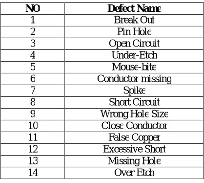
Two types of PCB defects are there functional and cosmetic defects [4]. Functional defects can seriously affects performance of PCB. There are 14 types of defects on single layer bare PCB as shown in table 1. Figure 1 shows grayscale image of single layer Bare PCB and figure 2 shows same image but with defects as mentioned in table 1.
Based on reviews of previous works, in 2002 Heriansyah [9] developed a PCB image segmentation algorithm by collecting well defined PCB Image generic patterns into four main segments using mathematical morphology and windowing technique. Laterin 2004, Heriansyah [10] classifies 12 out of the 14 known PCB defects by combining the segmentation of image with artificial neural network (ANN). Recently, Khalid [11] produced an image processing algorithm using MATLAB by subtracting the images and then X-OR operation is performed. The 14 defects are then grouped into 5 categories.
ISSN(Online): 2319-8753 ISSN (Print) : 2347-6710
I
nternational
J
ournal of
I
nnovative
R
esearch in
S
cience,
E
ngineering and
T
echnology
(An ISO 3297: 2007 Certified Organization)
Vol. 5, Issue 6, June 2016
Table 1. Defect on Single Layer Bare PCB
As shown in table 1. The types of defects available on PCB is of 14 types known defects as Break Out, Pin Hole, Open circuit, Short circuit, Spike, Close conductor, Missing hole etc. this defects are then can be combined into 5 categories.
III. METHODOLOGY
1. Image Segmentation
The algorithm which is used to segment the image into basic well defined generic patterns and classification have been developed based on the binary morphological image processing. After segmentation next step is to enclose each pattern so that pixels only under this window will be processed. The defect detection applied in this work is based on image subtraction operation.
The segmented well defined patterns of the reference image will be enclosed using the technique of windowing, and these window coordinates will be mapped onto test image to have the same window coordinates for the test image also. At the same time, the detected defects from the previous subtraction operation will also be enclosed using same windowing technique. Next step is assignment operation to define position of enclosed defect patterns Relative to enclosed test image patterns.
This research does the modification of the mathematical morphology for image segmentation in preparing the images for defect detection and classification. Template image is a grayscale image of perfect PCB without any defects and is used as reference image as in figure 1 and test image is a grayscale image of a defective PCB as shown in figure 2. which has been generated to have all 14 types of defects as listed in table 1. Both the template and test images are segmented into 4 segments each i.e. segment of square, segment of hole, segment of thick-line and segment of thin-line as in Figure 3 and Figure 4. The square segment has the image of square pads, the hole-segment has the image of hole pads, the thick-line segment has the image of thick conductors and the thin-line segment has the images of thin conductors.
Some of the defects only occur on particular segments of test image as wrong hole size, breakout and missing of hole for the hole segment and missing of conductor or open circuit for thin-line segment. Other defects might be exists in multiple segments. Mouse-bite and under- etch exist in both hole segment and square segment. By breaking the image into the clusters, some of the defects which are related to specific segments can be easily identified and classified.
NO Defect Name
1 Break Out
2 Pin Hole
3 Open Circuit
4 Under-Etch
5 Mouse-bite
6 Conductor missing
7 Spike
8 Short Circuit
9 Wrong Hole Size
10 Close Conductor
11 False Copper
12 Excessive Short
13 Missing Hole
ISSN(Online): 2319-8753 ISSN (Print) : 2347-6710
I
nternational
J
ournal of
I
nnovative
R
esearch in
S
cience,
E
ngineering and
T
echnology
(An ISO 3297: 2007 Certified Organization)
Vol. 5, Issue 6, June 2016
2. Image Processing Technique for PCB Detection and classification
Once the template image and test image is segmented, threshold values are determined for the grayscale images in order to convert images into binary. Grayscale images between 0 and 255 levels are converted into binary images only with two levels 0 and 1. This is to simplify further process.
Fig.3. Morphological Segmentation of Template Image [6]Fig.4. Morphological Segmentation of Test Image [6]
As shown in above fig 3. & fig 4. Both the template and test images are segmented into 4 segments each i.e. segment of square, segment of hole, segment of thick-line and segment of thin-line.
This project will not consider consistent binary convergence that can cause unwanted noise. It is observed that the unwanted noise occurs at regular intervals in the thin-line and thick-line segments which can be removed by using the median filtering. Then these binary images are given as input to the image processing algorithm through MATLAB tools. The algorithm uses following operations:
2.1 Image Difference Operation
Image difference is the simplest technique which involves comparing of two images pixel-by-pixel by using XOR logic operator.This image difference operation is also called as imagecomparison operation.The image difference operation is developed in order to get differences between the two images.
2.2NOT operator
NOT Operator is generally used for changing the image from black to white and vice versa. This operator is used to inverts the bit values of any variable.
2.3 Flood-fill Operator
The flood-fill operator is used to change the colour of the region. For binary images, flood-fill operator changes its connected background pixels to foreground pixels till it reaches object boundaries. This operator could be useful for the images to remove irrelevant artefacts. In this study, this operator is used to fill the holes in a binary image.
2.4 Image Subtraction
ISSN(Online): 2319-8753 ISSN (Print) : 2347-6710
I
nternational
J
ournal of
I
nnovative
R
esearch in
S
cience,
E
ngineering and
T
echnology
(An ISO 3297: 2007 Certified Organization)
Vol. 5, Issue 6, June 2016
the outcome of this operation is divided into positive and negative images.
2.5 Image Addition
Image addition is method of combining objects from two images into one image.In this project, addition operation combines the defects from one group and defects from another group in one image. This is achieved by using OR logic operator.The algorithm for image processing produces 5 new images for each pair of template and test images. Since the morphological segmentation algorithm is also able to produce 4 segmented images for both template and test image, thus, this algorithm is able to generate 4x5 images i.e. 20 images which will improve the ability of the system for overall defect detectionand classification.
By using defected patterns generated by above algorithm and defected PCB image we can locate those defects on PCB. Its advantage is it possible to tell where exactly defect has occurred, which not possible only seeing at defects.
IV. EXPERIMENTAL RESULTS
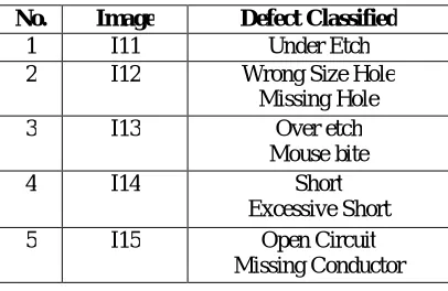
Based on exercises of several test and template images, an example of result obtained is shown in figure 5. From 20 images which were generated by the image processing algorithm, some images were identified as beneficial. The images are named I11, I12, I13, I14, and I15.
a) I11 b) I12c) I13
d) I14e) I15
Fig.5 (a-e). Classified Defect Images [6]
ISSN(Online): 2319-8753 ISSN (Print) : 2347-6710
I
nternational
J
ournal of
I
nnovative
R
esearch in
S
cience,
E
ngineering and
T
echnology
(An ISO 3297: 2007 Certified Organization)
Vol. 5, Issue 6, June 2016
take place so that the defect will be highlighted on the fine (original) image. The location will be superimposed on the original image with a red marker as shown in Figure 5 (a-e).
Table 2. Classified Defect Groups
Classification of defects are as shown in table 2. Defect in I11 is Under etch, in I12 is Missing hole or wrong size hole, in I13 is Over etch or mouse bite, in I14 is short or excessive short and inn I15 defect is open circuit or missing conductor.
V. CONCLUSION
From the above experiment, the given algorithm successfully detects and classifies defects into several groups. Due to these results, the proposed algorithm detects successfully several types the defects such as breakout, short circuit, wrong hole size, open circuit, close conductor, under etch, mouse bite, excessive short, missing conductor, missing hole, and over etch. After detecting defects localization of defects makes inspection easy and precise. The unwanted images also gets generated by noise during grayscale to binary conversion. Future improvement for this algorithm should include ability to detect and classify all 14 types of defects individually.
REFERENCES
[1]Ajay Pal Singh Chauhan, Sharat Chandra Bhardwaj, “Detection of Bare PCB Defects by Image Subtraction Method using Machine Vision,”Proceedings of the World Congress on Engineering 201, Volume 2, July 2011, London, U.K.
[2] M. Moganti, F. Ercal, C.H. Dagli, and S. Shunekawa, 'Automatic PCB Inspection Algorithm: A Survey', 1996, 63. No. 2.
[3] Z. Ibrahim, S.A.R AI-attas and Z. Aspar, 'Analysis of the WaveletBased Image Difference Algorithm for PCB Inspection', in proceedings of SICE, Osaka, Japan, 2002
[4] Wen-Yen Wu, Mao-Jiun J.Wang and Chih-Ming Liu, 'Automated Inspection of Printed Circuit Board Through Machine Vision', Computers in Industry, 28 (1996) pp.I03-III.
[5]F. Wang, X. Li and G. Xu, “The PCB Defect Inspection System Design Based on Lab Windows/CVI', International Conference on Industrial Mechatronics and Automation, ICIMA, 2009.
[6]Malge P.S., Nadaf R.S., “PCB Defect Detection, Classification and Localization using Mathematical Morphology and Image Processing Tools,” International Journal of Computer Applications (0975 – 8887), Volume 87, Number 9, February 2014.
[7]E. K. Teoh, D. P. Mital, B. W. Lee, and L. K. Wee, “Automated Visual Inspection of Surface Mount PCBs,” IECON '90., 16th Annual Conference of IEEE , pp. 27-30, November. 1990.
[8] Hong-Hai Loh, Ming-Sing Lu, “Printed Circuit Board Inspection Using Image Analysis,” IEEE Transactions on Industry Applications, vol. 35, no. 2, pp. 426-432, 1999
[9]R. Heriansyah, S.A.R AI-Attas, and M.M. Ahmad Zabidi, “Segmentation of PCB Images into Simple Generic Patterns usingMathematical Morphology and Windowing Technique”, Malaysia 2002
[10]R. Heriansyah. 'Classification of Defect on Bare PCB using Neural Network Technique', Masters Thesis, Universiti Teknologi
Malaysia.2004.
[11] N.K. Khalid. 'An Image Processing Approach Towards Classification of Defects on Printed Circuit Board', Projek Sarjana Muda, Universiti Teknologi Malaysia, 2007.
No. Image Defect Classified
1 I11 Under Etch
2 I12 Wrong Size Hole Missing Hole
3 I13 Over etch
Mouse bite
4 I14 Short
Excessive Short
5 I15 Open Circuit
![Fig.5 (a-e). Classified Defect Images [6]](https://thumb-us.123doks.com/thumbv2/123dok_us/1638031.1204550/5.595.69.508.416.691/fig-a-e-classified-defect-images.webp)