Process Simulation of Super Junction Power
MOSFET
Gaurav Saxena1, Shivani Saxena2, Shalini Jharia2
Assistant Professor, Department of Electronics and Communication Engineering, Poornima College of Engineering,
Jaipur, India1
Assistant Professor, Department of Electronics, Banasthali University, Niwai, Tonk, India2
ABSTRACT: This paper show a simple model for fabrication process of Super junction power MOSFET. The device dimensions, different regions, appropriate materials for each regions etc. are taken from literature to achieve desired property accordingly. The benefit for such type of modelling is to make fabrication process steps easier to understand. On the basis of some specific parameters like on-state resistance, break down voltage etc. a comparative study is also done to illustrate, the basic differences in Conventional Power MOS with Super junction Power MOS.
KEYWORDS: Power MOSFET, Super Junction MOSFET, SILVACO.
I . INTRODUCTION
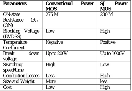
All the semiconductor devices like diodes, transistors, MOSFETs, JFETs, etc are used as a power devices. Among them all, MOS based power devices are most favourably used. A power MOSFET is a specific type of metal oxide semiconductor field-effect transistor (MOSFET) designed to handle significant power levels. Compared to the other power semiconductor devices, for example IGBT, Thyristor, its main advantages are high commutation speed and good efficiency at low voltages. But there are some mark able problems associated with them. Therefore, V shaped MOS, Double diffused MOS, U shaped MOS, Lateral MOS, Super Junction (SJ) MOS are used as power devices. VMOS has lowest ON-resistance and used at power up to 50V [1][2]. A Super junction Power MOSFET with breakdown voltage of 600V is compared with conventional Power MOSFET in following table I:
Table 1: Conventional Power MOS vs SJ Power MOSFET (600 V)
Parameters Conventional Power MOS
SJ Power MOS
ON-state Resistance (RDS
(ON)
275 MΩ 230 MΩ
Blocking Voltage (BVDSS)
Low High
Temperature Coefficient
Negative Positive
Break down voltage
Up to 200V Up to 1000V
Switching speed/time
High Low
The above comprehensive comparison shows that, due to charge balancing mechanism by using of n and p columns, SJ power MOS have low value of resistance, it results low conduction losses. Less area in SJ Power MOS make low value of capacitances also. The combination of low resistance and capacitance values, make less switching time and improved speed. Therefore, SJ power MOS now become favourable device in high frequency applications [3].
II. SUPER JUNCTION POWER MOSFET
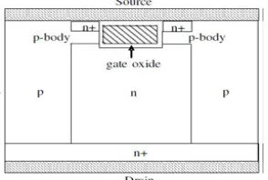
In the Super junction (SJ) power MOSFET structure, the heavily doped alternative p-n columns (or p-n pillars) are replaced by the lightly doped drift region of conventional power MOS. These p-n columns have the same doping level, therefore, they have equal amount of positive and negative charges. The numbers of such columns are applications specific. The middle column, for example, in SJ n-MOSFET, where n type doping column is just below the gate, called drift region, used as to form conduction path for charge carriers. By proper choosing the depth, width and doping profile for these regions, we can precisely controlled charges and so as, current due to positive and negative charges. A Schematic diagram of Super junction power MOSFET is shown in figure 1.The opposite sides of source and drain in SJ MOS structure support higher current and voltage.
Figure 1: Schematic View of Super Junction Power MOSFET [4]
To obtain the maximum break down voltage, drift region length and width is properly optimized. Electric field distribution in this region also support break down voltage. Uniform electric field increase break down of device [4].
III. DEVICE PARAMETERS FOR SJ MOSFET
The designing of SJ power MOSFET includes drift region engineering, i.e width, depth, doping and isolation from other regions. All dimensions are precisely controlled for particular voltage ratings. Another important design parameter is about trench, which is optimized for break down voltage. The correspond device parameters are mentioned in table 2:[5].
Table 2: Design parameters of SJ Power MOSFET for Simulation
Device Parameters SJ MOSFET
Cell pitch 12 um
Device height 43um
Device Width 18 um
For each n and p type Pillar height
36 um
For each n and p Pillar Width
6 um
Trench depth 36 um
Epitaxy layer thickness 42 um
From above table, we see that doping of n and p pillars/columns have exactly same doping level. This is charge balancing phenomena where equal amount of positive and negative charges are there. It results best performance in SJ power MOS [6] [7].
IV. SIMULATION & RESULTS
Here super junction Power MOSFET is fabricated by Deep Trench Etching where deep trenches of p type material is fabricated on n-type substrate [8]. The Super junction MOSFET fabrication process is starts with a moderately doped n+ - type (100) Si substrate with substrate dopant concentration of As 5x10¹⁸/cm3 .
(a) (b)
Figure 2: (a) An n-type epitaxial layer (36 um) is deposited on the entire surface, (b) Deposition of Oxide SiO2
(c) (d)
Figure 3: (c) Trench of 36 um were formed by using selective Reactive Ion Etching (RIE), (d), P-type layer was epitaxial grown to fill the trench using conformal deposition.
(e) (f)
(g) (h)
Figure 5: (g) Open a window for making p-type tub and deposition of 6 µm thick P-type layer, (h) Etched the entire top surface of p-type layer and removed all oxide, p-Pillar and n-Pillar were formed.
(i) (j)
Figure 6: (i) Deposition of oxide and open window for making p+ region. Implantation of Boron though the window in p-type tub and removed all oxide layer, (j) Deposition of oxide layer and window opening for making n+ region in p+ region and n-type impurity atom , phosphorus , are implanted through the window in the oxide and etched whole oxide. And thus the source region is defined [9], [10].
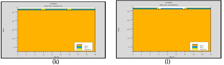
(k) (l)
(m) (n)
Figure 8: (m) Metallization of Aluminium, (n) Un-Wanted metal is etched and defined the electrodes for Source, Gate and Drain.
Figure 9: A two dimensional Super Junction MOSFET model
Above figure shows the final model of SJ MOSFET, where n and p columns are placed alternatively, which is differ from Conventional MOS [11], [12].
V. CONCLUSIONS
In conclusions, Super Junction Power MOSFET has been studied and complex fabrications process flow of such device has become simpler by easy going flow in SILVACO. The DECKBUILD tool of SILVACO is used for making this deep trench, n and p columns Super Junction Power MOSFET. For Modelling and simulation, appropriate data collection is very much important. This modelled structure is compared with another super junction power MOSFET which have different specifications and modelling style. This shows good agreement having simpler and more visualize method for model process flow.
REFERENCES
1. Surbhi Sharma, Vani gupta , Shivani saxena, “ A Review on VDMOS as a Power MOSFET”, International Conference proceeding IOSR Journal of Electronics and Communication Engineering, special issue-AETM’16, page no. 119-126.
2. Rakesh Vaid and Naresh Padha, “Comparative study of Power MOSFET devices structures”, Indian Journal of Pure & Applied Physics, Vol. 43, December 2005, pp.980-988.
3. Fujihira, T. Theory of Semiconductor Superjunction Devices. Jpn. J. Appl. Phys. Oct. 1997, vol.36, p.6254-6262.
4. Chen YU, “Design and Fabrication of Super Junction Power MOSFET Devices”, PhD thesis, National University of Singapore, 2008. 5. J. Dodge. “Power MOSFET Tutorial,” Application Note: APT-0403, pg. 1-12, March 2006.
6. P. N. Kondekar, M. B. Patil and C. D. Parikh, “ Analysis and Design of Superjunction Power MOSFET: CoolMOSTM for Improved On
Resistance and Breakdown Voltage Using Theory of Novel Voltage Sustaining Layer,” PROC. 23rd INTERNATIONAL CONFERENCE ON MICROELECTRONICS (MIEL 2002), VOL 1, NIŠ, YUGOSLAVIA, 12-15 MAY, 2002.
8. Raghavendra S. Saxena and M. Jagadesh Kumar, "Trench Gate Power MOSFET: Recent Advances and Innovations", Advances in Microelectronics and Photonics, Chapter 27,pp:1-23, 2012.
9. M. H. Juang, L. C. Sun, W. T. Chen, C. I. Ou-Yang, “A Process Simplification Scheme for Fabricating Self-aligned Silicided Trench-gate Power MOSFETs”, Solid State Electronics Vol. 45, 2001, pp. 169-172.
10. J.A. Yedinack et al., “Super-Junction Structures and Fabricating Methodologies for Power Devices,” Korean Patent: 10-2010-0083153. 11. Gerald Deboy, Florin Udrea,” Superjunction devices & technologies – Benefits and Limitations of a revolutionary step in power
electronics”,EPE 2007 – Aalborg, Denmark, 2–5 September 2007.