ABSTRACT
HEUSS, GREGORY PAUL. Thermal Stability of Transition Metal Nitrides as NMOS Gate Electrodes. (Under the direction of Dr. Veena Misra.)
Refractory metals and their nitrides are being considered as gate electrodes for scaled CMOS devices. The advantages of metal gates over doped polysilicon include the reduction of parasitic gate depletion, the elimination of the need for doping of the electrode, the potential compatibility with high-k dielectrics and reduced resistivity of the electrode. Simulations of scaled devices indicate a dual metal approach is necessary to achieve low and symmetric threshold voltages while maintaining gate control over the channel. The development of an NMOS compatible metal gate is especially challenging since the metals with appropriate work functions(~4eV) tend to be thermodynamically unstable on SiO2 and
promising high-K dielectrics.
This work focused on the impact of nitrogen on the Ta1-xNx/SiO2 system following
rapid thermal anneals up to 1000ºC. It was determined that the reaction in the Ta1-xNx/SiO2
system is fundamentally different than in the Ta/SiO2 system. Increasing the nitrogen content of the gate electrode improved the thermal stability of the metal/dielectric interface but did not change the work function of the electrode. The nitrogen content of the electrode was varied by controlling the partial pressure of nitrogen during the reactive sputtering of the films. The incorporation of nitrogen into the dielectric during gate electrode deposition and the redistribution of nitrogen during subsequent thermal treatments is expected to limit the use of metal nitrides as gate electrodes. Reactions in the Ta
1-xNx/SiO1-yNy materials system were investigated through electrical and analytical
Dedication
To my parents
Jon and Theresa Heuss
My brother
Steven Merrill Heuss
My wife
Meeta Loomba Heuss
And My daughter
Biography
Acknowledgements
There are many individuals who have contributed to this work either directly or
indirectly. First, I would like to thank my wife, Meeta, for her many years of support during this process. Next, I would like to thank my parents and in-laws for their encouragement.
To my advisor, Veena Misra, for believing in my abilities when I doubted myself. To Dennis Maher for always knowing how to refocus me or offer advice. To Gerry Lucovsky and Jon-Paul Maria for serving on my committee.
Table of Contents
List of Tables viii
List of Figures ix
1. INTRODUCTION 1
1.1 CMOS Technology Scaling
1.2 Why Are Metal Gates Required for
Future CMOS Devices
2
1.3 Selection Criteria for NMOS Gate Electrode
3
1.3.1 Work Function Requirements 4
1.3.2. Stability with Annealing 6
1.3.3. Carrier Concentration 8
1.3.4. Barrier to Oxygen Diffusion 8
1.4. Advantages and Disadvantages of
Metal Gate
8
1.5. Characterization of Advanced Gate Electrodes
10
1.6. Outline of Dissertation 11
2. TRANSITION METALS AND METAL NITRIDES AS GATE ELECTRODES
15
2.1. Thermal Stability 15
2.2. Refractory Metals 16
2.3. Refractory Metal Nitrides 28
3. PROPERTIES OF Ta AND Ta1-xNx THIN
FILMS
30
3.1. Introduction 30
3.2. Deposition Technique 31
3.3. Experimental 32
3.4. Deposition Rate 33
3.5. Metal to Non-Metal Ratio 33
3.6. Phase Identification 34
3.9. Resitivity 35
3.10. Carrier Concentration 36
3.11. Influence of Nitrogen on Barrier Properties
37
3.12. Oxidation Resistance of Ta1-xNx
During Annealing 37
3.13. Roughness of Ta1-xNx Films 38
3.14. Stability of Nitrogen in the Gate Stack
38
4. CHARACTERISTICS OF Ta1-xNx/SiO2/Si
SYSTEM 46
4.1. Introduction 46
4.2. Experimental 46
4.3. Work Function Extraction 47
4.4. Capacitance-Voltage Analysis 48
4.5.Work Function Extraction by CV Analysis
48
4.6. Frequency Dependence of Ta1-xNx
Gates on SiO2
51
4.7. Barrier Height Extraction by
Nordheim Analysis 51
4.8. Correlation of Work Function and
Barrier Height
52
4.9. Interface Characteristics of Ta1-xNx
on SiO2
54
4.10. Ta1-xNx on High-K Alternate
Dielectrics
54
5. THERMAL STABILITY OF Ta1-xNx GATE
ELECTRODES ON SiO2
68
5.1. Introduction 68
5.2. Selection of Temperatures for
Thermal Stability Evaluation 68
5.3. Experimental Details 69
5.4. Electrical Results … 69
5.5. Mechanism of Decrease in
Capacitance After Annealing 71
5.5.1. Role of Parasitics on
Voltage Measurements
71
5.5.2. Role of Area 72
5.6. Composition of Reaction Layer 76 5.7. Effective Circuit Model of Reaction
Layer
77
5.8. Flatband Voltage Stability: Work Function and Nitrogen Effects
79
5.9. Reliability of Dielectric 81
5.10. Ta1-xNx on HfO2 .. 82
6. CONCLUSIONS AND
RECOMMENDATIONS FOR FUTURE WORK
111
6.1. Conclusions 111
6.2. Recommendations for Future Work 112
List of Tables
page 1.1 Equivalent Oxide Thickness as Projected by the ITRS Roadmap…….…….. 13 3.1 Stoichiometry of Tantalum Nitride Films as a Function of the Partial N2 Flow
as Measured by AES ……… 33
4.1 Deposition Conditions and Work Function Extracted from C-V
Measurements……… 50
4.2 Work Function Extracted from C-V Measurements and Barrier Height
Extracted from Fowler-Nordheim Tunneling………... 52 5.1 Increase in Effective Dielectric Thickness is Independent of the Capacitor
Area ……….. 73
5.2 Total Charge within the Dielectric, Nf [C/Cm2] Calculated from the Slope of
List of Figures
page Figure 1.1 Increasing effect of polysilicon depeletion effect upon the gate
capacitance as the dielectric thickness is decreased. From Y. Taur, et.al., Proceedings of the IEEE, Vol. 58, No.4 1997………...
12
Figure 3.1 Ta-N phase diagram……… 39
Figure 3.2. Ratio of N:Ta as a function of the partial flow of N2 ………. 40
Figure 3.3. Resistivity (log scale) vs partial N
2 flow in Argon for as-deposited Ta
1-xNx films………
41
Figure 3.4. X-ray diffraction spectra of 550Å thick Ta1-xNx(5%) gate as a function
of anneal temperature……….. 42
Figure 3.5. X-ray diffraction spectra of 700Å thick Ta1-xNx(15%) gate as a
function of anneal temperature……… 43
Figure 3.6. X-ray diffraction spectra of 700Å thick Ta1-xNx(71%) gate as a
function of anneal temperature……… 44
Figure 3.7. Resistivity (4-point probe) as function of anneal temperature………… 45
Figure 4.1 Capacitance-voltage showing a positive shift in the flatband voltage
for a range of nitrogen stoichiometries relative to that of tantalum…… 55 Figure 4.2 Flatband voltage as a function of dielectric thickness for Ta
1-xNx(5,15and 71%) on SiO2 following forming gas anneal at 400ºC for
30min ………..
56
Figure 4.3 Schematic of the proposed model for nitrogen diffusion within the dielectric………..
57
Figure 4.4(a) High resolution transmission electron micrograph of an as-deposited Ta1-xNx(71%) gate electrode on SiO2………..
58
Figure 4.4(b) Electron energy loss spectroscopy spectra with oxygen and nitrogen ionization edges at three positions within the SiO2 region ……….
58
Figure 4.5 Density of interface traps at 400ºC FGA in the lower half of the band gap as determined by the conductance method. The average value of Dit has increased by three times with an increase in the partial flow of N2 from 15% to 25% during the reactive sputtering of a Ta1-xNx film...
59
Figure 4.6 Linear fit to flatband vs voltage curves for Ta,Ta1-xNx(5%), Ta1-xNx
(15%) and Ta1-xNx (71%) ………...
60
Figure 4.7 Frequency dependence (1MHz,100kHz,10kHz,1kHz) for
W/TaSixNy/Ta1-xNx (5%)/SiO2 following forming gas anneal ………...
61
Figure. 4.8 Frequency dependence (1MHz,100kHz,10kHz,1kHz) for
TaN(71%)/SiO2 following forming gas anneal with a large variation in
the transition region indicating high Dit ………... 62
Figure 4.10 Fowler-Nordheim plot in which the analytical expression for F-N tunneling is used to extract the barrier height from the experimental gate current-gate voltage ………
64
Figure 4.11 Comparison of the gate leakage as a function of nitrogen content of the gate electrode and dielectric ……….
65
Figure 4.12 Capacitance-voltage curves for Ta and Ta1-xNx on an RPECVD
deposited oxide and oxide/nitride stacked dielectrics ……… 66
Figure 4.13 High resolution transmission electron micrograph of Ta1-xNx(5%
flow)/SiO2/Si after a 400ºC anneal ……….
67
Figure 5.1 Capacitance-Voltage of W/Ta/SiO2 capacitor as a function of anneal temperature. Active area was 50µm x50µm and the frequency was 1MHz ………
83
Figure 5.2(a) HRTEM of Ta/SiO2 annealed at 900C ……….. 84 Figure 5.2(b) HRTEM of Ru-Ta alloy/SiO2 annealed at 900ºC ……….. 84
Figure 5.3(a) Capacitance-voltage curve for W/TaxN1-x(5% N2 flow)/SiO2 as a
function of anneal temperature. Active area was 50µmx50µm and the frequency was 1MHz ……….
85
Figure 5.3(b) Capacitance-voltage curve for W/TaxN1-x(15% N2 flow)/SiO2 as a
function of anneal temperature. Active area was 50µmx50µm and the frequency was 1MHz ……….
86
Figure 5.3(c) Capacitance-voltage curve for W/TaxN1-x(71% N2 flow)/SiO2 as a
function of anneal temperature. Active area was 50µmx50µm and the frequency was 1MHz ……….
87
Figure 5.4 Change in Cet as a function of anneal temperature for Ta, Ta1-xNx
(5,15 and 71%) ………... 88
Figure 5.5 Capacitance-Voltage curves as a function of frequency for TaN(5%) gate following forming gas anneal at 400C ………...
89
Figure 5.6 Capacitance-Voltage curves as a function of frequency for TaN(5%) gate following forming gas anneal at 1000C ……….…
90
Figure 5.7 Auger Electron Spectroscopy Depth Profile of as-deposited
W/TaN(5%)/SiO2/Si ………...
91
Figure 5.8 Auger Electron Spectroscopy Depth Profile of W/TaN(5%)/SiO2/Si annealed at 1000C for 15s in Argon ………...
92
Figure 5.9 Capacitance-Voltage curves for TaN(5%) gate. Active area is 300µm x 300µm at a frequency of 1MHz ………..
93
Figure 5.10(a) Gate current density (Jg) vs Oxide Voltage (Vox) for TaN(5%) gate ... 94 Figure 5.10(b) Gate current density (Jg) vs Oxide Voltage (Vox) for TaN(5%) gate ... 95 Figure 5.11 Gate current density (Jg) vs Oxide Voltage (Vox) for TaN(5%) gate
on n-type substrate ………. 96
Figure 5.12 Change in Eot from 400C to 1000C for gate electrode
TaN(5%),TaN(15%),TaN(71%) on SiO2 at 1MHz ………
Figure 5.13 High resolution transmission electron micrograph of a W/ Ta1-xNx
(5%)/SiO2/Si capacitor annealed at 1000C for 15 sec in Argon ………..
98
Figure 5.14 Effective circuit model of gate stack following high temperature anneal ……….
99
Figure 5.15 Model of composite dielectric following high temperature anneal …… 100 Figure 5.16 SIMS profile of nitrogen through the SiO2 dielectric for both
TaN(5%) and TaN(71%) gate in the as-deposited state and following an anneal at 1000C ……….
101
Figure 5.17(a) Linear fit to Vfb-Eot curves for TaN(5%),(15%) and (71%) gates on SiO2 annealed at 400C. Measurement frequency-1MHz ………
102
Figure 5.17(b) Linear fit to Vfb-Eot curves for TaN(5%),(15%) and (71%) gates on SiO2 annealed at 700C. Measurement frequency-1MHz ………
103
Figure 5.17(c) Linear fit to Vfb-Eot curves for TaN(5%),(15%) and (71%) gates on SiO2 annealed at 900C. Measurement frequency-1MHz ………
104
Figure 5.17(d) Linear fit to Vfb-Eot curves for TaN(5%),(15%) and (71%) gates on SiO2 annealed at 1000C. Measurement frequency-1MHz
………...
105
Figure 5.18(a) Vfb-Eot for TaN(5%) gate on SiO2 as a function of anneal
temperature. Measurement frequency-1MHz ……… 106
Figure 5.18(b) Vfb-Eot for TaN(15%) gate on SiO2 as a function of anneal
temperture. Measurement frequency-1MHz ……….. 107 Figure 5.18(c) Vfb-Eot for TaN(71%) gate on SiO2 as a function of anneal
temperture. Measurement frequency-1MHz ……….. 108
Figure 5.19 Capacitance-voltage curves for three gate electrodes on HfO2 ……….. 109
Figure 5.20 Change in Eot(relative to Eot at 400C) following a rapid thermal anneal ……….
Chapter 1. Introduction
1.1 CMOS Technology Scaling
In the early stages of microelectronics, metals were used as gate electrodes for
transistors. Doped polysilicon gates replaced metal gates because they simplified the
fabrication process by allowing self-aligned source and drain while simultaneously
doping the gate all under high temperature processing. The use of self-aligned doped
polysilicon gates decreases the overlap capacitance between gate and the source and
drain. Polysilicon also allowed the use of ion implantation to obtain different
workfunctions for NMOS and PMOS devices by placing appropriate dopants in the
polysilicon gates.
Since then, the semiconductor industry has undergone an aggressive scaling ritual.
Specifically, the scaling of minimum feature sizes, such as the channel length, has been
the major driving force for improving circuit speed, reducing power dissipation and
increasing packing density. Table 1.1 shows the equivalent oxide thickness (EOT) for
SiO2 gate insulator as a function of lithographic dimensions as proposed in the recently
According to projections made in the NTRS, sub-1nm gate oxide is required for 50nm
and beyond IC devices to maximize gate control and improve short channel effects.
Unfortunately, the scaling of SiO2 below 1.5nm is plagued by several key
challenges. These include: (i) the gate leakage current through the gate oxide increases
exponentially with decreasing gate thickness; (ii) inadequate reliability for SiO2 below
1.5nm; (iii) boron penetration in PMOSFETs surface-channel with P+ gate increases
significantly, and (iv) increased effect of polysilicon depletion[1]. New materials have to
be introduced in the basic CMOS structure to replace the existing ones to enable
continued scaling of devices because of the limitations of SiO2 and polysilicon.
An efficient way to reduce leakage current is to use a high dielectric constant K,
or high-K dielectric film. High-K films allow the use of a physically thicker film while
electrically behaving as a thin dielectric. A material such as ZrO2 with a dielectric
constant around 20 can be made about 5 times thicker than SiO2 for the same SiO2
equivalent oxide thickness, which is easy to control and manufacture. A physically
thicker film would increase the tunneling barrier, thus decreasing the gate leakage. Such
high-K materials would offer significant reductions in tunneling currents while still
producing low teq.
1.2 Why are Metal Gates Required for Future CMOS Devices?
Typical polysilicon gates suffer from a depletion effect when the gate is biased to
invert the channel region. The voltage drop across the polysilicon gate leads to an
increase in Eot of 3-4 Å in addition to that due to the physical thickness of the dielectric.
an order of magnitude lower than the doping concentration of a metal electrode. The
impact of poly-depletion has been insignificant for SiO2 thicknesses larger than 40Å
since its effect was undetectable. However, as the dielectric thickness is reduced, the
poly-depletion effect becomes a larger fraction of the Eot and the need for heavily doped
polysilicon gates or metallic gates becomes imperative. Fig 1.1 shows the deviation of
inversion capacitance from the accumulation capacitance with poly-silicon gates and
metal gates. Metal gates eliminate the gate depletion problem thereby allowing the full
benefit of scaled gate dielectrics.
Another motivation for metal gates is the reduction of the problem of autodoping
of boron due to penetration through the dielectric. Since metal gates will not require
dopant implantation, the problem of dopant diffusion through thin dielectrics to the
underlying substrate is precluded.
It is has also been reported that polysilicon based electrodes can react with
emerging high-K dielectrics producing silicides. For example, it has been reported that
polysilicon deposition at higher temperatures results in the reduction of ZrO2 to form a
Zr-rich layer near the electrode/dielectric interface. This layer leads to shifts in the
flatband voltage and higher leakage currents.
1.3 Selection Criteria for NMOS Gate Electrode
The selection criteria used in this work were based on the integration of metal
gates into a conventional planar CMOS process flow. The selection criteria are i) work
function; ii) thermal stability; iii) carrier concentration, and iv) oxygen diffusion barrier
Most of the research on high-K dielectrics has employed an inert gate electrode
such as Pt and Au. This approach allows the dielectric to be characterized for critical
properties such as leakage current mechanism, while leaving the details of the interaction
with a realistic gate electrode to be determined later. However, several issues such as
cost, film stress and lithography limit their attractiveness. Moreover, the gate electrode
and dielectric are interdependent and must be optimized concurrently. To date, there is
not yet a consensus on the high-K dielectric that will be used for planar CMOS beyond
100nm devices. In addition, the gate electrode-dielectric system should be scalable for a
several generations of devices to offset the cost of new processing equipment.
1.3.1 Work Function Requirements
The gate electrode work function necessary to achieve low and symmetric
threshold voltages is dependent on other device parameters. The following discussion
pertains to the required work functions for planar bulk CMOS devices.
The threshold voltage of a device is a function of the potential of the gate
electrode (Φm), potential of the substrate (Φs) and the total charge within the dielectric.
Low threshold voltages are desired for low power and high performance applications. For
short channel devices, the geometry of the components of the device impacts the
threshold voltage[2]. Since the doping of the channel region must be increased to reduce
short channel effects, the preferred means of obtaining the desired work function is by
setting the work function of the gate electrode since this allows a larger doping
concentration in the channel. In order to replace n+ and p+ poly-Si while maintaining
respectively within 0.2 eV of the conduction and valence band edges of Si[3]. It should
be noted that midgap work function metals (e.g., TiN and W) are inadequate for
advanced devices due to a) threshold voltages that are too large for low-voltage
operation; or b) severely degraded short channel characteristics due to low substrate
doping density.
The advantage of polysilicon gates, in terms of work function, has been the
simplicity of one deposition step followed by two ion implantation/diffusion of dopants
to form the small (near Ec) and large (near Ev) work functions. In order to incorporate
metal gates into current CMOS technology, a dual metal gate system is required which
will significantly increase the complexity of gate electrode formation for both nFET and
pFET. The integration challenges will be discussed further.
Any alternative to polysilicon must have a work fuction near Ec for NMOS and a
work function near Ev for PMOS. Table 1.2 indicates the work function of known metal
and metal alloys. The metallic elements with vacuum work function near the conduction
band of silicon include Al, Hf, Zr, Ti and La. Metallic gate electrodes, including metal
nitrides, metal silicides, have intrinsic work functions that span the range from 3.5-5.3eV.
Transition metals tend to have work functions between 3.9 and 4.4eV. Noble metals tend
to have work functions near 5eV. Work function values are also related to their
electro-negativity. Once a metal is used as a gate electrode, an effective work function is the
more appropriate parameter since the measured work function will be a superposition of
the intrinsic work function and any dipoles at the electrode/dielectric interface.
Elemental metals have an intrinsic work function but a dipole at the metal/dielectric
magnitude of the dipole may be different for the same metal electrode on different
dielectrics.
Silicon-on-insulator (SOI) devices and double gate devices may have different
work function requirements than bulk CMOS devices[4]. In the case of fully depleted
SOI devices where the channel is intrinsically doped, the desired gate electrode work
function may be closer to mid-gap.
1.3.2 Stability with Annealing
Although the work functions of these metals fulfill the first of the required
attributes, the requirement of being stable in contact with the dielectric is not fulfilled in
all cases. Since electronegativity, which is related to free energy of formation, is
proportional to its work function, elemental metals with lower work functions (NMOS
compatible) have problems with stability. Metals such as Ta, Ti, Al, Zr, Hf are
considered inadequate for gate application under conventional process flows since they
react with the underlying dielectric. As will be shown in Chapter 2, Zr, Hf, and Ti tend to
reduce underlying dielectrics, resulting in higher gate leakage currents. Moreover,
reaction with elemental metals and SiO2 may result in silicide bonds at the dielectric
interface, which tend to drive the work function closer to mid-gap. It should be noted
that, although some low work function elemental metals may be thermodynamically
stable on high-K dielectrics (ZrO2), the high oxygen affinity of these metals makes it
impossible to avoid interface oxidation, leading to an EOT increase. Elemental metals
with larger work functions, such as Ru, Pt, Au, on the other hand, provide intrinsic
The challenge is in finding low work function metals, which also offer good
thermal stability. The thermal stability of these low work function metals can be
improved by the addition of a second, or a even a third element. For example, the
addition of N in metals can effectively reduce reaction rates, provide better diffusion
barrier properties and result in smoother microstructures. These metal nitrides can be
potential NMOS gate electrode candidates provided the presence of N and Si does not
increase the work function. In this work, Ta1-xNx gate was explored because it is the most
stable of the metal nitrides in which the metal has a work function near Ec. Metal alloys
such as TaN have all been studied as barrier layers for Cu interconnection and have
shown superior diffusion barrier properties [7]. The addition of Si or even another metal
to form an alloy is another means of increasing the stability of the gate electrode. It
should be noted that the presence of silicon in the gate electrode can result in silicide
bonds at the dielectric interface which will tend to drive the work function closer to
mid-gap.
The effective MOS work function of the gate electrode should not be sensitive to
small changes in composition of the gate electrode. Since the formation of a compound
or alloy may be necessary to suppress the reaction with the gate dielectric, the degree of
control of the gate electrode stoichiometry is important. The gate electrode must react
with the dielectric to facilitate bonding, but the reaction should not continue beyond the
top few monolayers of the dielectric. The mechanical forces involved with the rapid
thermal annealing of the gate-dielectric interface can result in adhesion problems.
Although a ‘gate last’ processes would reduce the thermal stability requirement, it
1.3.3 Carrier Concentration
Most metals and metal alloys have very high carrier concentrations. However, the
introduction of excess N and/or Si into metals results in high resistivity. Although high
resistivity metals are considered undesirable for interconnect applications, they can still
be used for gate electrode applications provided their carrier concentration is high. The
carrier concentration will primarily determine the degree of gate depletion.
1.3.4 Barrier to Oxygen Diffusion
To maintain an Eot during annealing cycles post gate electrode deposition, the gate
electrode should be a barrier to oxygen transport. For example, platinum gates are
transparent to oxygen and therefore result in significant interfacial SiO2 growth when
placed on high-K dielectrics and annealed under high temperatures. This is undesirable as
it leads to a decrease of the gate capacitance. The affinity of refractory metals for oxygen
is a factor in the metal-SiO2 reaction[5, 6].
The oxygen barrier properties of metals can be improved by the addition of N
and/or Si. It must be noted that, although a capping layer placed on top of the electrode
can avoid oxygen diffusion from the ambient, it does not prevent oxygen diffusion from
the sidewalls of the gate electrode.
The primary motivation for moving to metallic gate electrodes is the significant
reduction in the polysilicon depletion effect (PDE) when the gate is biased in inversion.
However, this comes at the cost of increased integration complexity. While the
replacement of SiO2 with a high-K dielectric does not change the integration flow, the
incorporation of dual work function metals greatly increases the integration complexity.
Unlike dual polysilicon gate technologies in which a single polysilicon layer is deposited
and then implanted, dual metal gates will most likely require two separate metal
deposition steps. To avoid damaging the underlying dielectric of the region in which the
first metal is removed, the deposition of the dielectric will accompany the deposition of
the second metal. Another non-critical photo step will be needed to remove the second
metal and the dielectric from the first metal region (alternatively, CMP can be used to
planarize and remove the dielectric). This results in a net addition of two non-critical
photo steps.
There are alternate routes available. For example, if a metal can be implanted
with a certain atom that alters its work function to the desired value, then a process flow
similar to polysilicon can be obtained. Recently, it has been demonstrated that Mo can be
implanted with N to result in a higher work function film[ ]. Another integration route
may involve the deposition of a metal stack consisting of metals A and B followed by the
removal of the top metal B from one of the well regions. A reaction, either diffusion or
intermixing, between the two metals can be controlled to produce a counter work
function compared to the region in which only metal A exists. This methodology would
performance gained by use of metal gates will be able to justify the addition of either one
or two non-critical photo steps.
1.5 Characterization of Advance Gate Electrodes
Many characterization techniques are available for evaluating emerging gate
stacks to obtain their physical, electrical and chemical nature. Electrical characterization
techniques including C-V and I-V were performed on MOS capacitors to obtain relevant
parameters such as flat band voltage, average interface trap density, as well as reliability
parameters such as charge to breakdown, and time to breakdown. These parameters are
directly related to the dielectric and gate electrode properties, and are therefore used to
evaluate the quality of the gate stack.
Moreover, these parameters can be tracked as a function of high temperature
treatments to monitor the interface reactions of the gate stack. For example, utilizing a
Vfb vs Eot curve can provide information on the work function of the electrode, changes
in the Eot, the charge contained within the dielectric and the distribution of the charge
within the dielectric. Any reaction layers that are formed may contain components of
resistance and capacitance and these are in series with the underlying dielectric.
Therefore, frequency dependence must be utilized to differentiate between different
layers. The conductance technique can provide an accurate interface state density value
for ultra-thin dielectrics.
Materials analysis techniques must also be used to understand the physical
makeup of the gate stack and to corroborate with the electrical results. The analytical
electron spectroscopy (AES) depth profiling for determining stoichiometry and elemental
profiles, high resolution scanning tunneling electron microscopy(HRTEM) and electron
energy loss spectroscopy(EELS) for physical measurements of films thicknesses and
elemental profiles through the films and secondary ion mass spectrometry(SIMS) for
profiling nitrogen within the dielectric.
1.6 Outline of Dissertation
The objective of this work was to evaluate transition metal nitrides as gate
electrodes. Through the use of electrical and analytical methods, the structure and
composition of Ta1-xNx gate electrodes were correlated to the interface and bulk reactions
occurring following a high temperature anneal.
This chapter introduced the motivation for evaluating metal gates and provided
reasons for using Ta1-xNx as a NMOS gate electrode. The next chapter will present some
experimental results on elemental low work function metals and their instabilities on
SiO2. Chapter 3 will then discuss the materials analysis of Ta1-xNx gates on SiO2 and
how the deposition process can impact the properties of the underlying dielectric.
Chapter 4 will discuss the electrical properties of Ta1-xNx on SiO2 and on HfO2 under low
temperature conditions. This chapter will also discuss the nitrogen diffusion problems
associated with metal nitrides. Chapter 5 will discuss the high temperature stability of
Ta1-xNx gates and how it depends on the nitrogen concentration and temperature. A
model of a reaction layer will be presented. Electrical results of Ta1-xNx gates on HfO2
will also be presented. Finally, Chapter 6 will summarize the conclusions of this work
Figure 1.1. Increasing effect of polysilicon depeletion effect upon the gate capacitance as the dielectric thickness is decreased.
Year of Production
Equivalent physical oxide thickness, Tox [nm]
2001 2002 2003 2004 2005 2006 2007 2010 2013 2016
1.3-1.6 1.2-1.6 1.1-1.6 0.9-14. 0.8-1.3 0.7-1.2 0.6-1.1 0.5-0.8 0.4-0.6 0.4-0.5
Table 1.1. ITRS predictions for the equivalent oxide thickness, Tox[nm] for scaled logic
devices. Nodes highlights in red indicate new solutions are required to meet these
Chapter 2. Transition Metals and Metal Nitrides as
Gate Electrodes
This chapter will discuss the metals and metal compounds that have work
functions appropriate for use as NMOS gate electrodes. Although low work function
metals (~4eV) are numerous, the feasibility of a metal for use as a gate electrode requires
thermal stability with the dielectric at temperatures of 900-1000ºC. Refractory transition
metals and compounds of these metals are of interest because they have high melting
points and form stable compounds.
The work function values for transition metals used as electrodes in MOS devices
varies tremendously. This variation is partially due to the different techniques used to
determine the work function of the electrode. The work function of TiN on Ta2O5 was
reported to be 4.95 eV while the work function on SiO2 was determined to be 4.3 eV[7].
Whether the incorporation of nitrogen increases the work function of the gate
electrode or merely creates charges in the dielectric is a matter of controversy in the
literature. Wakabayashi et al concluded that the work function of TiNx decreases as the
concentration of nitrogen is increased[8]. Nitridation of the gate oxide during the
deposition of the gate electrode has been observed in the WNx/SiO2 system by Moriwaki
et al[9]. The incorporation of nitrogen into the top layers of the dielectric tends to reduce
2.1 Thermal Stability
One of the primary requirements of a gate electrode is that it not react with the
dielectric beyond the bonding necessary for adhesion to the dielectric. Juxtaposition of a
metal and dielectric will often lead to undesired reactions because the placement of
chemically different atoms in close proximity leads to atomic migration in order to lower
the overall free energy and establish equilibrium [Kaloyeros, Annu. Rev. Mater. Sci.
2000. 30:363-85]. The reaction layer can either be insulating or conducting and can
correspondingly affect the Eot and the Vfb shift of the device. Therefore the gate
electrode should be chemically inert and structurally stable.
2.2 Refractory Metals
Many of the low work function metals are thermodynamically unstable on SiO2.
The reactivity of a wide range of metals, including Zr, Hf and Ti, with SiO2 was
determined experimentally by Pretorius et al[10]. Thermodynamics provides an
explanation for the reactions between refractory metals and SiO2. Beyers used ternary
phase diagrams of Mo,W, Ta, Ti-silicon-oxygen systems to explain the observed
reactions[11]. The following paper discusses the limited thermal stability of two metals,
which have appropriate work functions but react with SiO2.
The temperature at which Ta react with SiO2 varies in the literature.
Thermodynamic calculations indicate there is a small driving force for the reaction
The Use of Metal Oxide Semiconductor Capacitors to Detect
Interaction of Hf and Zr Gate Electrodes with SiO
2and ZrO
2Introduction
As silicon complementary metal oxide semiconductor devices (MOS) are scaled
below 100 nm, advanced high-K gate dielectrics will be required to obtain oxide
equivalent thickness, Tox-eq, < 1.0 nm. As Tox-eq decreases, the capacitance associated with
the depletion layer at the polycrystalline-Si-gate dielectric interface becomes increasingly
important, making it necessary to consider alternative gate electrodes, such as metals
[1,2]. The search for metallic gates faces many challenges since they must have
appropriate work functions, be stable with the gate dielectric during subsequent high
temperature processing steps and thermal/chemical interface stability with dielectrics. To
replace n+ and p+ polycrystalline silicon and maintain scaled performance, it is necessary
to identify pairs of metals with workfunctions that are respectively within 0.2 eV of the
conduction and valence band edges of Si, i.e., the workfunction, m, for N-channel and
P-channel gates must be near 4eV and 5eV, respectively [3].
In this work, we have investigated the properties of hafnium and zirconium gate
electrodes on SiO2 and high-K dielectrics. The motivation behind selecting these gates is
based on their low workfunction values appropriate for NMOS devices. It has been
reported that both Zr and Hf have workfunction values near 4.0 eV [ ]. Moreover, no
prior reports on the electrical properties of Hf and Zr metals as gate electrodes exist on
either SiO2 or emerging high-K dielectrics. Since emerging high-K dielectrics include
ZrO2, HfO2 or ZrSiO4, it is very timely to evaluate the properties of Zr and Hf gate on
Experimental
Field oxide isolated overlap capacitors were fabricated on n and p-type wafers
using lift-off to define the gate electrodes. Thermal oxide controls of varying thicknesses
were grown at 900ºC. ZrO2 and Zr-silicate dielectrics were formed using MOCVD of
C16H36O4Zr. An in-situ sputtered tungsten capping layer was deposited following the Hf
and Zr deposition to ensure contact to the underlying layer and to avoid oxidation of Hf
and Zr electrodes. The base pressure of the chamber in which the metal films were
deposited was < 2x10⁻⁸ Torr. Following gate definition the samples were annealed in
10%H2/N2 for 30 minutes. An HP4284A was used to measure the capacitance-voltage
characteristics. The capacitor area of the devices measured was 2.5x10⁻⁵ cm2. The
flat-band voltage and equivalent oxide thickness for the capacitors were extracted from C-V
curves using Dr. Hauser’s C-V analysis program [5].
Results and Discussion
Fig. 1 shows the capacitance vs. voltage curves for SiO2 dielectrics with Hf gates
for various anneal conditions. The as-deposited condition retains some sputtering
damage and therefore results in a VFB shift from the expected VFB. The capacitance value
of the as-deposited case resulted in a Tox that matched the physical thickness of the grown
SiO2. After a 400ºC anneal, the VFB moved to the appropriate value for Hf gates
indicating that the sputtering damage was removed. However, the accumulation
capacitance value dramatically increased indicating that Tox was considerably thinner
than the as-grown thickness. Anneals done at 500ºC further increased the capacitance
larger increases of accumulation capacitance values. The inset of Fig. 1 displays the gate
leakage current as a function of the gate voltage of the same samples. As shown, the
leakage current increases indicating that as the capacitance increases, the leakage current
through the gate dielectric also increases. In order to verify whether the changes in
leakage current are coming entirely from the physical thickness reduction of the SiO2,
Fowler-Nordheim tunneling current modeling assuming a typical effective mass of
0.42mo was performed. A barrier height of 3.2eV was chosen based on the workfunction
values ( m~ 4 eV) obtained from our capacitance-voltage curves, which also agrees with
the bulk workfunction values published in literature for Hafnium. If the oxide thickness
as obtained from the C-V curve was used, the modeled leakage current was significantly
higher than the experimental data, indicating that the physical thickness of the stack is
larger than the electrical thickness value obtained from C-V. This indicates that the
reduction in SiO2 is being accompanied by the formation of a high-K layer. To
understand this, cross-sectional transmission electron microscopy was performed on
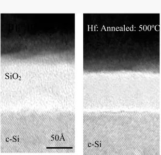
un-annealed and un-annealed (500ºC) Hf gates and the results are shown in Fig. 2. As shown,
that along with a physical thinning of the SiO2 layer after a 500ºC anneal there is also the
presence of an amorphous layer between the Hf and the SiO2 regions. If the physical
oxide TEM thickness (obtained by adding both the light and dark regions) is used in the
current voltage modeling, then a much more reasonable fit is obtained to the measured
data, although accurate analysis would involve knowledge of effective mass within the
high-layer and all the band offsets. An average barrier height, obtained by extracting the
slope of J/Eox2 vs. 1/Eox curves, resulted in a barrier height value of 2.9eV, close to the
obtained from TEM results in an excellent fit to the experimental data thereby verifying
the presence of a high-K layer.
In order to obtain compositional information of the interface layer between the Hf
and the SiO2, XPS depth profiling was performed. Near the gate electrode and dielectric
interface, we obtained a mixture of signals including primarily Hf-O bonds with some
Hf-Si bonding. The inherent limitation of XPS analysis prevented the accurate
identification of this layer, however the above leakage current analysis suggests the
presence of a high-K dielectric.
The capacitance increase effect on SiO2 with Hf gate electrode as a function of
various starting thicknesses is quantified in Fig. 3. As shown, a starting thickness of 50Å
was reduced to ~10Å even under a very moderate temperature anneal of 400ºC/30min
+500ºC/30min. The same phenomenon was also observed with Zr gates that were
subjected to similar temperature anneals.
To understand the mechanisms behind the reduction of SiO2 at such low
temperatures (400ºC-500ºC), it is insightful to investigate the role of oxygen solubility of
these metals. It has been reported that metals such as Zr, Hf, Ti and V have very high
oxygen solubility and high negative free energy of formation of oxide and can easily
reduce SiO2 at temperatures higher than 650ºC. In fact, it has been reported that these
when these metals are placed on SiO2 and annealed above a critical temperature, they
result in the formation of a mono-silicide adjacent to the SiO2 and metal oxide on top [6].
This is attributed to the reduction of SiO2 in the presence of the metal atoms. The released
oxygen then diffuses from the dielectric-metal interface upward to the metal electrode
near the electrode-dielectric interface reacts with the metal atoms to form a silicide
region. This reaction continues until the metal region on top is completely converted to a
metal oxide. In our work, we have found that the reduction of the SiO2 is occurring at
temperatures as low as 400ºC, significantly lower than reported earlier. One possible
reason why earlier work did not detect any reaction at such low temperatures maybe
related to the use of Rutherford back scattering (RBS) to detect reaction layers and the
use of very thick SiO2 films. RBS does not have the resolution to detect reaction layers
that are < 150Å. Since capacitance is sensitive to changes in thickness on the order of
Angstroms, the use of MOS capacitors provides a very sensitive tool to measure changes
in dielectric at the gate electrode/dielectric interface. Any change in either VFB or Cox
would indicate a reaction layer at the gate electrode-dielectric interface. The use of these
extremely high sensitivity MOS capacitors has allowed us to detect reactions between
SiO2 and Hf and Zr gates occurring at temperatures as low as 400ºC. The RBS analysis
in reference [6] indicated that the interfacial layer was primarily a monosilicide.
However, RBS is known for its poor oxygen sensitivity and may not accurately reflect
the composition of this layer. As discussed earlier, our XPS analysis of the interfacial
region revealed the presence of oxygen in the form of Hf-O bonds. Furthermore,
current-voltage analysis also supported the presence of a high-K dielectric layer between the Hf
and SiO2. A complete chemical analysis of the interface layers would require more
sensitive techniques such as EELS.
In order to evaluate the above metal gates on high-K dielectrics, Hf and Zr gates were
also evaluated on ZrO2 and ZrSixOy MOS capacitors. In this case, the gatestacks
capacitance values. The leakage of these high-K gatestack films was extremely high
following the anneal. The explanation of the instability of Hf and Zr on ZrO2 dielectrics
can also be explained by high oxygen solubility of these metals. When these metals are
in contact with dielectrics such as ZrO2, the oxygen from the dielectrics can easily spread
out in the metal forming a metal-oxygen solid solution. This effect has in fact been
observed when Ti is placed in TiO2, Zr on ZrO2 and Ta on Ta2O5 [6,7]. It should be noted
that if the anneal temperatures are low then the oxygen can only redistribute and dissolve
but not chemically react.
In summary, we have evaluated Zr and Hf gate electrodes on SiO2 and high-K
dielectrics annealed under modest temperatures. MOS capacitor results indicated drastic
instabilities of both Hf and Zr gates on all dielectrics studied. The decrease in electrical
thickness was attributed to a combination of both SiO2 reduction and high-K layer
formation. This was attributed to the high oxygen solubility of these metals, which can
reduce the dielectrics underneath and scavenge their oxygen. These metals have very
high negative enthalpy of formation, which indicates their ease of oxidation. Therefore
gate metals such as Zr, Hf, Ti, V etc, will display severe instabilities on dielectrics such
References
1. J.R. Hauser and W.T. Lynch, Critical Front End Materials and
Processes for 50nm and beyond Devices, SCR Working Paper, 1997.
2. Semiconductor Industry Association. International Technology
Roadmap for Semiconductors: 1999 edition. SEMATECH, 1999.
3. I. De, D. Johri, A. Srivastava, C.M. Osburn, Solid State Electron. 44,
1077 (2000)
4. H.B. Michaelson, “ Relation between an atomic electronegativity scale
and the workfunction, “ IBM J. Res. Dev. 22, 72, 1978.
5. J. R. Hauser and K. Ahmed, “Characterization of ultrathin oxides using
electrical C-V and I-V measurements, “Characterization and Metrology
for ULSI Technology, Edited by D.G. Seiler, A. C. Diebold, W. M.
Bullis, T. J. Shaffner, R. McDonald and E. J. Walters, AIP Conf. Proc.
449, 1998.
6. S.Q. Wang, J.W. Mayer, “Reactions of Zr thin films with SiO2
substrates”, J. of Appl. Phys. 64 (9), 1 Nov., pp. 4711, 1988
7. M. Berti, A.V. Drigo, C. Cohen, J. Siejka, G. G. Bentini, R. Nipoti, and
S. Guerri, “Titanium silicide formation: Effect of oxygen distribution in
Fig. 1 Capacitance-voltage change of SiO2 dielectrics with Hafnium electrodes
subjected to various annealing conditions. The inset shows the corresponding
gate current changes. 1x10-11
2x10-11 3x10-11 4x10-11 5x10-11
-4 -3 -2 -1 0 1 2
40 0 C / 30 m in. & 50 0 C / 30 m in . 500 C / 3 0m in .
40 0 C / 30 m in . A s d ep osite d
C a p a c it a n c e [ F ar ad s]
G ate V olta ge [V olts] 1 0-13 1 0-11 10-9 10-7 -15 -10 -5 0 G a te C u rre n t [A m p s ]
Fig. 2 Cross-sectional transmission electron micrograph of Hf gates on SiO2 for
as-deposited and after a 500ºC anneal. The TEM indicates the physical reduction
of the SiO2 layer after anneal which agrees with the electrical data. 0
20 40 60 80 100 120
As deposited 400C/30min 500C/30min 400C/30min +
500C/30
E
q
u
ival
en
t O
x
id
e
T
h
ic
k
n
es
s
[A
]
Fig. 3 Quantification of the oxide thickness reduction with Hf gates as a function of
various starting thicknesses and anneal temperatures.
[1] Hf:
As-d
it d
Hf: Annealed: 500ºC
c-Si
c-Si
SiO
22.3 Refractory Metal Nitrides
As discussed in the preceding paper, low work function elemental metals have
limited thermal stability on oxygen containing dielectrics. One approach to increasing the
thermal stability of these metals is the addition of nitrogen. Refractory metal nitrides
have been shown to increase the critical temperature for reactions with materials such as
crystalline silicon[13]. The structure of metal nitride often consists of close packed metal
atoms with nitrogen occupying octahedral interstitial positions. The metal nitrides are
referred to as interstitial alloys because of the interstitial locations of the nitrogen atoms.
Bonding in metal nitrides is due to the interaction of nitrogen 2s and 2p orbitals with the
metal d orbitals [3]. The direction of charge transfer is from nitrogen to metal. The
bonds in metal nitrides have covalent and metallic components.
Ideal stoichiometry is not often realized for refractory metal nitrides. The phases
exist over a wide range of compositions and large fractions of the non-metal lattice sites
are vacant with a smaller fraction of the metal lattice sites vacant. The vacancy
concentration has a significant impact on the thermodynamic, electrical and mechanical
properties of these films. Different deposition techniques tend to result in different defect
structures which explains why the properties of metal nitride films vary so greatly in the
literature.
Of the refractory metal nitrides, tantalum nitride is the most promising for NMOS
gate electrode applications because of the combination of low work function, excellent
diffusion barrier properties and high melting point. TaN and WN have been found to
block the diffusion of oxygen better than TiN[14]. The work function values for Ta1-xNx
using methods that are fundamentally flawed. For instance, the work function of the gate
electrodes can not be calculated from a single C-V curve since the flatband voltage
includes charges within the dielectric. In the following chapters, details of Ta1-xNx
deposition parameters, film properties, electrical characteristics and thermal stability will
be presented. The change of Eot and Vfb will be used as tools to assess the stability of
Ta1-xNx gates. Finally, the properties if Ta1-xNx gate electrodes will be correlated with the
Chapter 3. Properties of Ta and Ta
xN
1-xThin
Films
3.1
Introduction
The inclusion of nitrogen to the lattice of tantalum enhances the properties of the
film as a gate electrode. Tantalum nitride is less susceptible to oxidation than
tantalum[15]. Sputtered tantalum films dissolve 12 atomic percent oxygen with a
different degree of suboxide formation than bulk tantalum. The oxide grows as a dense
and adherent amorphous phase with parabolic oxidation kinetics.
As mentioned previously, the temperature at which metal nitrides reacts with
other films can be greatly increased relative to the elemental metals. The reported body of
work on Ta and TaN has primarily focused on Cu diffusion studies, which have a few
similarities to the requirements of gate electrodes[16]. In other studies it has been
reported that the reaction temperature of possible Ta- silicide formation was increased by
several hundred degrees using TaN[13]. Most researchers have studied the phases of Ta
1-xNx by sputtering Ta in increasing N flow rates and observed the formation of products of
the two layers being separated by the diffusion barrier.
In this chapter, the main requirements of an optimal gate electrode will be used as
a guideline in discussing issues related to the deposition of TaN films. The required
ambient during steps subsequent to the gate electrode formation. A gate electrode
candidate must possess all of these attributes. Since the first monolayers of the gate
electrode determine the important parameter φms, the interface between the gate electrode
and the dielectric is critical. The electrical properties of a metallic gate electrode are
influenced by a range of structural and chemical characteristics. This chapter will discuss
how the metal to non-metal ratio in metal compounds, N diffusion during film deposition,
diffusion barrier properties etc. impact the electrical properties and microstructure of the
film. This chapter will provide details about the structural and chemical properties for
films with Ta1-xNx where x ranged from 0 to 0.6.
3.2 Deposition Techniques
The deposition of the gate electrode must not degrade the properties of the
underlying dielectric. Although deposition parameters such as pressure and rf power are
mentioned in the literature, the ion bombardment energy and ion flux are rarely reported.
The reason for the variability of film properties between systems is most likely due to
differences in the ion bombardment energy and ion flux to the substrate[17].
Reactive RF sputtering was the deposition technique selected because of the ease
varying the Ta:N ratio by changing the partial pressure of nitrogen in the sputtering
ambient. Sputtering exposes the dielectric to energetic charged and neutral species that
may damage the dielectric. Reactive sputtering in N2 and Ar results in nitrogen species
with high energies due to its small mass. The incorporation of nitrogen atoms into the
gate dielectric during reactive sputtering is a limitation of the technique. Sputtering
power, partial pressure of N2, the sputtering gas species, and pressure within the system
and bias of the substrate. The use of xenon to sputter tantalum onto thermal SiO2 has
been shown to increase the reliability over the same gate material sputtered using argon
ions[18].
Other deposition techniques that have been shown to reduce the amount of
damage created during gate electrode deposition include chemical vapor deposition. A
comparison of PVD and CVD of TiN gates[ ] showed that the reliability of the devices
with CVD gates was considerably greater than the PVD gate deposited onto the same
dielectric. CVD has another advantage over PVD in that conformal films are possible
which may eventually be necessary if a transistor structure requires deposition onto a
vertical surface. However, CVD processes typically have unwanted elements, such as
halides or carbon, which can degrade the oxide characteristics.
3.3 Experimental
The Ta1-xNx films were deposited using a magnetron reactive sputtering
deposition reactor with base pressure <1x10⁻⁸ Torr. The target was pre-sputtered in Argon
for 25 minutes to clean the surface. The Ta1-xNx films were sputtered in varying N flow
rates. The nitrogen purity was 99.999%. Low oxygen content thin films are obtained by
using extremely high purity sputtering gas sources and sputtering under ultra-high
vacuum conditions. The RF power was kept constant during the various N2 flow rates.
The chosen power was 50 Watts which corresponded to a power density of 2.4 W/cm2.
An in-situ tungsten(500 Å)/TaSiN(250Å) stack was deposited on top of the Ta1-xNx films
characterization. The films were then subjected to various anneal conditions and
analyzed via several materials analysis methods.
Of the ten different Ta1-xNx gate conditions evaluated, the three following gate
stoichiometries are representative of the different types of gates.
Table 3.1. Stoichiometry of tantalum nitride films as a function of the partial N2 flow as
measured by AES.
Partial N2 flow in Argon Ta1-xNx
5% Ta0.6N0.4
15% Ta0.52N0.48
71% Ta0.46N0.54
3.4 Deposition Rate
The deposition rate is a function of the nitrogen partial pressure during sputtering.
The film thickness was measured using a Dektak surface profiler. The deposition rate
was found to decrease from 25 to 4 Å/min for N2 flow rates of 0% to 71%, respectively.
The decrease of deposition rate could be attributed a) saturation of the Ta target by N
atoms which leads to lower Ta sputter rate. It should be noted that the deposition rate
dependence on N2 flow is also a strong function of process parameters such as RF-power
The Ta-N phase diagram shown in Figure 3.1 displays single-phase regions for
several stoichiometric compounds including Ta2N and TaN. Tantalum nitrides are defect
compound structures with a range of atomic concentration of N allowed in the stable
phases. The various phases in the Ta-N system include β-Ta2N, θ-TaN, η-TaN, δ-TaN1-x,
Ta5N6, Ta4N5, Ta3N5[19]. Within each single-phase region, a finite range of nitrogen
content can be accommodated in the lattice of Ta atoms. As the nitrogen content is
increased, the metal lattice expands to accommodate the interstitial nitrogen until a
critical point is reached and a different structure is energetically favored.
The metal (Ta) to nonmetal (N) ratio of the Ta1-xNx films deposited was
determined using RBS and AES depth profiling. Rutherford Back Scattering is an
absolute measurement that is based on the energy of 3MeV He+ ions reflected from the
sample. The relationship between nitrogen flow rate and nitrogen content is shown in
Figure 3.3. Beyond a nitrogen partial flow of ~10% the nitrogen incorporation saturates.
In this high flow regime the sputtering target is ‘poisoned’, meaning that the surface of
the target is covered with nitrogen.
3.6 Phase Determination
The morphology of the film is a function of the nitrogen content, temperature of
the substrate, energies of the atomic flux and structure of the substrate. The crystalline
structures of the as-deposited and annealed Ta1-xNx films (400ºC,700ºC,900ºC,1000ºC)
were analyzed using θ-2θ x-ray diffractometry with a CuKα source at 40kV and 30mA
and is shown in Figure 3.4 (a) and (b). The as-deposited films were polycrystalline with
The Ta1-xNx films had a columnar grain structure due to the low adatom mobility under
the deposition conditions. As is evident from the phase diagram, there are nitrogen
compositions that are between stable compounds and thus result in a mixture of phases.
Multiple crystalline phases were observed for films all of the stoichiometries examined.
3.7 Nature of the Ta-N Bonds
The presence nitrogen in interstitial positions within the lattice of Ta atoms
increases the strength of the Ta-Ta bonds. Nitrogen atoms share electrons with the
neighboring Ta atoms. Takeyama et al. observed an increase in binding energy of Ta
with increasing nitrogen content indicating that the nature of the Ta-N bond is a function
of the stoichiometry [ ].
3.8 Stress of as-deposited and annealed films
Thermal stresses in thin films can cause poor adhesion, cracking or strain the
underlying dielectric. Metal often have larger thermal expansion coefficient than the
silicon substrate resulting in stresses within the dielectric and metal film. Both the sign
and magnitude of residual stresses can vary with the thickness of the metal film. Very
thin metal films often have a higher stress state than a slightly thicker film. No
mechicanl deformation of the metal films was observed following rapid thermal
annealing. The minimum capacitance was monitored for any changes following RTA
since Cmin is dependent on the effective active area but is independent of parameters
Annealing a metal film may change the total stress. Devices with tungsten gate
electrodes annealed at 1000ºC increased the fixed oxide charge density(Nf) and interface
state density (Dit) as observed by Matsuhashi et al[20].
3.9 Resistivity
The resistivity of the gate electrode should be as low as possible. The ITRS
Roadmap specifies a sheet resistance for the gate electrode. A high resistivity gate
electrode may be still be usable if a thin film is deposited to set the work function and a
lower resistivity metal is deposited on top to reduce the sheet resistance of the gate. The
bulk resistivity of Ta is 13 µΩ▪cm but the resistivity of thin films of Ta can be as high as
80-100 µΩ▪cm depending on the phase of the film. The hetero-epitaxial growth of low
resistivity bcc-Ta on Ta2N is a possible approach to creating a low sheet resistance
electrode with improved thermal stability[21]. The resistivity of Ta1-xNx films is
primarily a function of the Ta:N ratio, with secondary factors such as grain size having an
influence. The resistivity remains fairly constant with the addition of nitrogen until the
ratio of N:Ta becomes close to 1:1 at which point the resistivity increases dramatically
with increased nitrogen concentration.
Resistivity is a function of the grain size and impurity(eg. oxygen) levels for thin
metal films. The resistivity of metal-rich Ta1-xNx films increases slowly with increasing
nitrogen content[19]. The resistivity of nitrogen rich tantalum nitrides increases more per
atomic percent nitrogen than metal rich films. Some nitrogen rich films deposited in this
work exceeded the measurements capabilities of the four-point probe. The temperature
3.10 Carrier Concentration
One of the primary motivations for the use of metal gate electrodes is the
elimination of parasitic depletion effects that are a fundamental limitation of doped
polysilicon gates. Simulations have indicated that the poly depletion has a larger effect
on the gate capacitance as the dieletric thickness is reduced.
The carrier concentrations of Ta1-xNx films were measured using Hall mobility
measurements. The sign of the carrier concentration indicated that the majority carriers
were holes. This has been observed for metal silicides including TaSi2[].
3.11 Influence of nitrogen on barrier properties
One of the required characteristics of a metal gate electrode for conventional
process flow is thermal stability with the dielectric at temperatures of 900-1000ºC. Since
refractory compounds such as tantalum nitride have been utilized as diffusion barriers,
previous work on materials systems in which nitrogen increases the temperature stability
are relevant to the development of a gate electrode. There are several ways in which a
layer can act as a diffusion barrier. The requirement that the barrier be chemically inert is
the one relevant to the selection of a gate electrode. Since the electrode must adhere to
the dielectric some degree of chemical bonding must occur. As the N:Ta ratio is
increased the activation energy for the reaction between Ta1-xNx and SiO2 is expected to
increase. As will be discussed in chapter 5, we have observed an increase in the critical
3.12 Oxidation Resistance of Ta
1-xN
xDuring Annealing
The gate electrode/dielectric stack must be resistant to oxidation during post
deposition thermal cycles. The gate electrodes studied were composed of 200 Å of Ta
1-xNx with in-situ films of 250Å TaSiN followed by tungsten 400Å thick. Auger depth
profiling was used to monitor the oxidation of the gate stack upon annealing up to 1000ºC
in Argon. The top 40Å of the W capping layer had oxidized following the anneal in
forming gas at 400C for 30 min. An additional 150Å of the tungsten layer had oxidized
during an anneal at 1000ºC for 15 seconds in Argon. Note that the bulk of the gate stack
did not contain any oxygen following the rapid thermal anneal at 1000ºC.
Capping layers are necessary to prevent the oxidation TaN. Tantalum and
tantalum nitride oxidize quite readily when exposed to oxygen. It has been reported that
the TaN films with N/Ta ratios below 0.45 can be easily oxidized resulting in an increase
in resistivity of the film [ ]. This was directly correlated to the microstructure of the film
and polycrystalline TaN films suffered from ease of oxidation. When the N level was
increased enough to obtain an amorphous structure the oxidation resistance of the Ta1-xNx
films increased. Oxygen solubility impacts the interface reactivity of Ta1-xNx with SiO2
under high temperatures in chapter 5.
3.13 Rougness of Ta
1-xN
xFilms
Measurement of the RMS roughness of the top surface of the gate electrode films
after annealing can be used to infer the roughness at the interface with the dielectric.
As was mentioned earlier, nitrogen species can enter the dielectric region during
the Ta1-xNx deposition where it can create additional charge in the dielectric. In addition,
the nitrogen loss from the gate electrode under high temperature annealing is an
important issue since the released N can create adhesion problems of the gate with the
dielectric and promote further diffusion of N into the gate dielectric. The XRD peaks of
Ta1-xNx as a function of temperature are shown in Figure 3.5 and indicate no change of
peaks in the spectra indicating stability of the film. This also agrees with reported studies
that Ta1-xNx films, unlike WNx, do not lose their N when subjected to high temperatures.
0
0.2
0.4
0.6
0.8
1
1.2
0
20
40
60
80
100
AES
N/
T
a,
At
om
ic
R
at
io
Percent Flow, N2/(N2+Ar)
1.00E+00 1.00E+01 1.00E+02 1.00E+03 1.00E+04 1.00E+05 1.00E+06 1.00E+07
0 2.5 5 6.25 7.5 10 15
N
2partial flow
Re
si
stivity [
µ
Ohm
*c
m
]
Figure 3.3. Resistivity (log scale) vs partial N2 flow in Argon for as-deposited Ta1-xNx
0 100 200 300 400
20 30 40 50 60 70 80
Ta_15%_Deposited in Dr. Lucovsky's cluster tool
M10-2-4_2 M10-2-4_3 M10-2-4_4 M10-2-4_5
M10-2_700 M10-2_700 M10-2_700
M10-2_900 M10-2_900 M10-2_900
M10-2_1000 M10-2_1000 M10-2_1000C
In
ten
si
ty [a.
u.]
2-theta
Figure 3.4 X-ray diffraction spectra of 550Å thick Ta1-xNx(5%)
gate as a function of anneal temperature 400 C
700 C 900 C
0 50 100 150 200 250 300
20 30 40 50 60 70 80
Ta_deposited in Dr. Lucovsky's 3in. cluster tool
M10-1-4 M10-1-4_2 M10-1-4_3 M10-1-4_4 M10-1-4_5 M10-1_70 M10-1_71 M10-1_72 M10-1_900 M10-1_900 M10-1_900 M10-1_10 M10-1_11 M10-1_12 In te ns ity [a .u .] 2-theta 400 700 900 1000
Figure 3.5 X-ray diffraction spectra of 700Å thick Ta1-xNx(15%)
0 20 40 60 80 100 120
20 30 40 50 60 70 80
Ta_71%_Deposited in Dr. Lucovsky's 3in. cluster tool
M10-3-4_1 M10-3-4_2 M10-3-4_3 M10-3-4_4 M10-3-4_5 M10-3-7_4 M10-3-7_3 M10-3-7_2 M10-3-9_4 M10-3-9_3 M10-3-9_2 In te ns ity [a .u .] 2-theta 400 700 1000
Figure 3.6 X-ray diffraction spectra of 700Å thick Ta1-xNx(71%)