Design Simulation Analysis and Comparison
of 2-Way Wilkinson Power Divider with
Different Topologies
Kajol Jain
1, Abhishek Singh
21,M.Tech Research Scholar [Embedded System & VLSI Design], Dept. of ETE, Gyan Ganga Institute of Technology &
Sciences, Jabalpur, Madhya Pradesh, India
2Asst. Professor, Dept. of ETE, Gyan Ganga Institute of Technology & Sciences, Jabalpur, Madhya Pradesh, India
ABSTRACT: This paper presents 2 way Wilkinson power divider (WPD) on microstrip line proposed designed and
analysed for 650 MHz operating frequency. This Wilkinson power divider use elliptical as well as circular split design.
First an optimized 2 way elliptical splitWilkinson power divider is designed and the output response of this power
divider needs to be improved for equal and unequal both type of Wilkinson power divider applications. Then a circular
split designWilkinson power divider is presented that yields acceptable input and output responses for equal and
unequal Wilkinson power divider. This study shows the improvement of output simulation responses, this WPD have a
better isolation and insertion loss, and also give a better return loss of input and output ports for operating frequency at 650 MHz.All simulations are carried out by AWR simulator.
KEYWORDS: Wilkinson power divider(WPD), elliptical splitWilkinson power divider, circular split Wilkinson
power divider,Advancing the wireless revolution (AWR)
I. INTRODUCTION
Power divider and combiner is passive device that divide RF input power among several output and vice versa. The
power divider and power combiner are very popular components for a microwave power combining system. High power solid state RF power divider/combiner are essential due to modest power of solid state devices. As such, most of the popular powers combining schemes have emerged from communication system requirement; generally, a passive power divider can work as a power combiner without any modification due to the reciprocity Hence concepts developed for the power divider equally applies to a combiner. In case of power division, an input signal is divided
into two (or more) output signals of lesser power, while a power combiner as name suggests do reverse operation and
combines them at an output port. Power dividers usually provide equal and unequal power division ratio. In many
applications, there is a need to use microstrip Wilkinson power divider with unequal power division ratio. However, for the unequal Wilkinson power divider with high power dividing ratio,the characteristic impedance of one of the microstrip lines becomes high.
Figure 1 Basic Diagram of Power Divider/Combiner
II. RELATED WORK
The most popular and widely adopted power combining structure was proposed by E.J. Wilkinson in, 1960 and it is
These can reduce the dimensions of the divider and have a better return loss, insertion loss and isolation.In [1] author designs a 4:1 unequal Wilkinson power divider using a microstrip. The conventional Wilkinson topology is used for design with the defected ground structure (DGS) which can obtain the 4:1 power dividing ratio easily without any problem. Author in [2] investigated different type of microwave combining techniques like chain and tree combining and n-way combining structures. In the work of [3] focus of author was on the design, fabrication, and testing of feeding the networks individually and within an array system. In the design of Wilkinson power divider, three topologies, viz. straight split section, a circular split section, and an elliptical split section for the quarter-lambda split transmission line section were discussed. The elliptical split transmission line design results the most reduced size, but was rejected, due to close spacing of the lines did not allow themselves to be sufficiently decoupled from each other, and the circular and straight line quarter lambda split sections are designed, analysed and compared from simulation results. Ansoft HFSS simulator is used to compare these two topologies by simulation results.Another scheme was presented in [4] a uniform asymmetrical microstrip coupled lines was introduced to overcome the narrow strip width in unequal Wilkinson power divider with high dividing ratio. A comprehensive analytical design scheme is given in [5]; author has generalized unequal Wilkinson power divider operating at dual-frequency. Here, the parallel and series RLC
structures are chosen to obtain effective isolation between the two output ports according to different operating
frequencies. Paper [6] presents design and fabrication of 2way Wilkinson power divider (WPD) for dual operating Frequencies; 2.4GHz and 4.928GHz. This power divider has two branches of impedance transformer and parallel
connection at the output ports of this divider with RLC lumped element.The report [7] discusses both equal and
unequal power split cases. That is a power division ratio of 1:1, 3:2, 2:1 are discussed here. The circuits of 3 ports Wilkinson power divider are analysed by the author to reduce the size of it by replacing the λ/4 transmission line with a compact stepped impedance transmission line using even and odd mode analysis. The results show that matching at all the ports are good. And good isolation between output ports is achieved at designed frequencies.
Here, we describe a new topology to design power divider. The analysis of Wilkinson power divider and comparison
between Both topologies elliptical as well as circular split design are also presented. To demonstrate that circular split
design of Wilkinson circuit has a good performance in the equal, unequal both case, the proposed Wilkinson power divider has been analysed and simulated. The simulated results indicate reasonable agreement with the designed results.
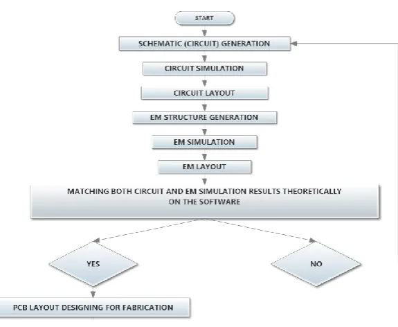
III.PROPOSED ALGORITHM
IV.DESCRIPTIONOFTHEDESIGNALGORITHM
Aim of the proposed algorithm is to Design simulate analyse and compare of 2-Way Wilkinson Power Divider with
different topologies; elliptical as well as circular split design. Two design topologies were simulated for the equal and
1:2 unequal WPD by, the elliptical split design and circular split design section. The design algorithm is consists of
three main steps. Steps to be followed:
1)
Design the power divider for the power division ratio K2 using design formula.2)
Calculate the Physical length and width of each microstrip line3)
Construct circuit and measure the performance parameters such as Input Return lossInsertion loss to port – 2 Insertion loss to port – 3, Isolation between two output ports
V. SIMULATIONRESULTSANDDISCUSSION
A. TWO WAY EQUAL POWER DIVIDERS
STEP 1:- Calculation of Equal Power Divider (i)
K2 = 1/1 , K=1
(ii) Z
02 = Z03 , Z02 = Z03 = 70.71ohm
(iii) R = 100 ohm
Where:-
K = Coupling factor
Z02 =impedance of port 2,Z03=impedance of port 3
STEP 2:- Calculation Of Width And Length Of Microstrip
AWR provides a TXLINE Calc utility to calculate the width, w and length, l in mm, according to your specifications. Using TXLINE Calc:
For Z0=50 Ohm, at λ/4 W= 7.2 mm, L= 69.39 mm
For Z= √2Z0=70.71 Ohm at λ/4 W= 3.9 mm, L= 71.08 mm
STEP 3:-Follow the Design Procedure
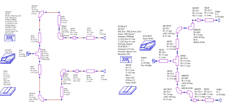
SCHEMATIC DESIGN
Figure 3 Schematic Diagram Of Equal (A) Elliptical And (B) Circular Spilt Power Divider
EM LAYOUT
Figure 4 EM Layout Of Equal (A) Elliptical And (B) Circular Spilt Power Divider.
.
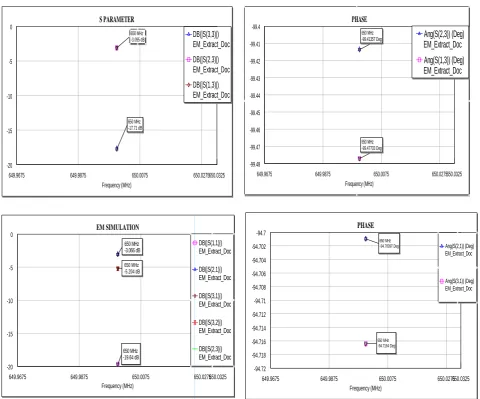
Figure 5: Graph of Equal (A) Elliptical and (B) Circular Spilt Power Divider. 3
1
2
3 2
1
649.9675 649.9875 650.0075 650.0275650.0325 Frequency (MHz)
S PARAMETER
-20 -15 -10 -5 0
650 MHz -3.095 dB
650 MHz -17.71 dB
DB(|S(3,3)|) EM_Extract_Doc
DB(|S(2,3)|) EM_Extract_Doc
DB(|S(1,3)|) EM_Extract_Doc
649.9675 649.9875 650.0075 650.0275650.0325 Frequency (MHz)
PHASE
-99.48 -99.47 -99.46 -99.45 -99.44 -99.43 -99.42 -99.41 -99.4
650 MHz -99.47703 Deg 650 MHz
-99.41357 Deg Ang(S(2,3)) (Deg)
EM_Extract_Doc Ang(S(1,3)) (Deg) EM_Extract_Doc
649.9675 649.9875 650.0075 650.0275650.0325 Frequency (MHz)
EM SIMULATION
-20 -15 -10 -5 0
650 MHz -5.204 dB
650 MHz -3.066 dB
650 MHz -19.64 dB
DB(|S(1,1)|) EM_Extract_Doc
DB(|S(2,1)|) EM_Extract_Doc
DB(|S(3,1)|) EM_Extract_Doc
DB(|S(3,2)|) EM_Extract_Doc
DB(|S(2,3)|) EM_Extract_Doc
649.9675 649.9875 650.0075 650.0275650.0325 Frequency (MHz)
PHASE
-94.72 -94.718 -94.716 -94.714 -94.712 -94.71 -94.708 -94.706 -94.704 -94.702 -94.7
650 MHz -94.7164 Deg
650 MHz
-94.70097 Deg Ang(S(2,1)) (Deg) EM_Extract_Doc
This divider is simulated using AWR simulators. Graphs shows the obtained scattering parameters achieved over the frequency of 650 MHz. An input return loss better than -20 dB is obtained over a frequency of 650 MHz. Moreover, the coupling coefficient equals to -3dB.
SIMULATION RESULTS OFEQUALELLIPTICALSPLITDESIGNVERSUSCIRCULARSPLITDESIGN
The following graph show the simulation result of return loss and insertion loss of elliptical as well as circular split
equal power divider. From the graph, it is observed that circular split equal WPD return loss is highly desirable and the
insertion loss is low when compared with elliptical split equal WPD. Figure (a),(b) shows the return loss of about -17.71dB and -19.64dB respectively.
ELLIPTICAL SPLIT DESIGN CIRCULAR SPLIT DESIGN
S PARAMETER SIMULATION RESULT S PARAMETER SIMULATION RESULT
650 MHz MAGNITUDE(dB) PHASE (Deg) 650 MHz MAGNITUDE (dB) PHASE (Deg)
S33 -17.71 dB S11 -19.64 dB
S23 -3.095 dB -99.410 S21 -3.066 dB 94.7000
S13 -3.095 dB -99.470 S31 -3.066 dB 94.7160
B. 1:2 UNEQUAL POWER DIVIDER
STEP 1:- Calculation and Simulation of 1:2 Unequal Power Divider
K2 = 1/2
K = .7071
Z02 = Z03 K2 , Z02 = 51.48
Z03 = Z0
1+𝑘2
𝑘3 , Z03 = 102.99
R = Z0 (K+1/K), R = 106.06
R02= Z0K, R02= 35.35
R03= Z0/K, R03= 70.71
Where:K = Coupling factor,Z02 =impedance of port 2,Z03 =impedance of port 3,R02 = resistance of port 2,R03 =
resistance of port 3
STEP 2:- Calculation of Width and Length of Microstrip:-
AWR to calculate the width, w and length, l in mm, according to our specifications. Using TXLINE Calc:
For Z0=50 Ohm, at λ/4 W=7.2 mm, L= 69.39mm
For Z02= Z03 K2=51.48 Ohm at λ/4 W= 6.84 mm, L= 69.52mm
For Z03= Z0
1+𝑘2
𝑘3 = 102.99 Ohm at λ/4 W= 1.64 mm, L= 72.87 mm
SCHEMATIC DESIGN:-
Figure6: Schematic Diagram of 1:2 Unequal (A) Elliptical and (B) Circular Spilt Power Divider
EM LAYOUT:
Figure 7: EM Layout of 1:2 Unequal (A) Elliptical and (B) Circular Spilt Power Divider.
MLIN ID=TL2 W=5.4 mm L=8 mm MLIN ID=TL3 W=1.6 mm L=57.2 mm MLIN ID=TL5 W=6.8 mm L=69.5 mm MLIN ID=TL6 W=9.4 mm L=47 mm MCURVE ID=TL9 W=1.6 mm ANG=180 Deg R=5 mm MBEND ID=MS3 W=9.4 mm ANG=90 Deg M=0 MSUB=SUB1 MBEND ID=MS1 W=5.4 mm ANG=90 Deg M=0 MSUB=SUB1 MLIN ID=TL7 W=9.4 mm L=6 mm MLIN ID=TL4 W=5.4 mm L=62.2 mm MSUB Er=3.5 H=3.2 mm T=.035 mm Rho=1 Tand=0 ErNom=3.5 Name=SUB1 1 2 3 MTEE ID=TL11 W1=6.8 mm W2=1.6 mm W3=7.2 mm MLIN ID=TL8 W=7.2 mm L=10 mm MLIN ID=TL14 W=7.2 mm L=2 mm MSTEP ID=TL10 W1=5.4 mm W2=1.6 mm MSTEP ID=TL15 W1=7.2 mm W2=5.4 mm MLIN ID=TL13 W=7.2 mm L=2 mm MSTEP ID=TL16 W1=9.4 mm W2=7.2 mm MSTEP ID=TL12 W1=9.4 mm W2=6.8 mm MCURVE ID=TL1 W=9.4 mm ANG=180 Deg R=5 mm EXTRACT ID=EX1 EM_Doc="EM_Extract_Doc" Name="EM_Extract" Simulator=EMSight X_Cell_Size=0.1 mm Y_Cell_Size=0.1 mm PortType=Default STACKUP="" Extension=2.54 mm Override_Options=Yes Hierarchy=Off STACKUP Name=SUB2 PORT1 P=1 Z=50 Ohm Pwr=40 dBm PORT P=2 Z=50 Ohm PORT P=3 Z=50 Ohm EXTRACT ID=EX1 EM_Doc="EM_Extract_Doc" Name="EM_Extract" Simulator=EMSight X_Cell_Size=0.1 mm Y_Cell_Size=0.1 mm PortType=Default STACKUP="" Extension=2.54 mm Override_Options=Yes Hierarchy=Off MCURVE ID=TL1 W=6.8 mm ANG=180 Deg R=20 mm MCURVE ID=TL9 W=1.6 mm ANG=180 Deg R=20 mm MLIN ID=TL2 W=6.8 mm L=6.8 mm MLIN ID=TL3 W=5.4 mm L=70.2 mm MLIN ID=TL4 W=1.6 mm L=10.1 mm MLIN ID=TL6 W=9.4 mm L=68.6 mm MLIN ID=TL8 W=7.2 mm L=2 mm MLIN ID=TL13 W=7.2 mm L=3.6 mm MLIN ID=TL14 W=7.2 mm L=4.6 mm MSTEP ID=TL5 W1=5.4 mm W2=1.6 mm MSTEP ID=TL7 W1=7.2 mm W2=9.4 mm MSTEP ID=TL15 W1=7.2 mm W2=5.4 mm MSTEP ID=TL21 W1=9.4 mm W2=6.8 mm MSUB Er=3.5 H=3.2 mm T=0.035 mm Rho=1 Tand=0.002 ErNom=3.5 Name=SUB1 1 2 3 MTEE ID=TL11 W1=6.8 mm W2=1.6 mm W3=7.2 mm STACKUP Name=SUB2 MBEND ID=MS1 W=1.6 mm ANG=90 Deg M=0 MSUB=SUB1 MBEND ID=MS3 W=6.8 mm ANG=90 Deg M=0 MSUB=SUB1 PORT1 P=1 Z=50 Ohm Pwr=40 dBm PORT P=2 Z=50 Ohm PORT P=3 Z=50 Ohm 3 2 1 3 2 1
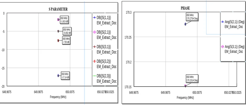
649.9675 649.9875 650.0075 650.0275650.0325 Frequency (MHz) S PARAMETER -20 -15 -10 -5 0 650 MHz -7.55 dB 650 MHz -5.002 dB 650 MHz -1.815 dB 650 MHz -17.14 dB DB(|S(1,1)|) EM_Extract_Doc DB(|S(2,1)|) EM_Extract_Doc DB(|S(3,1)|) EM_Extract_Doc DB(|S(3,2)|) EM_Extract_Doc DB(|S(2,3)|) EM_Extract_Doc
Figure 8: Graph of 1:2 Unequal (A) Elliptical and (B) Circular Spilt Power Divider
The results of the project were in agreement to the theoretical available results, so the various S parameters were plotted as shown above.The circuit’s main S-parameters were plotted S11,S12,S23 and S31. These indicate matching, power division, and port isolation, respectively.
SIMULATION RESULTS OF UNEQUAL ELLIPTICAL SPLIT DESIGN VERSUS CIRCULAR SPLIT
DESIGN
Table1 gives the performance analysis of circular split unequal WPD over elliptical split unequal WPD on the basis of insertion loss and return loss at the operating frequency. Elliptical split unequal WPD return loss is measured of about -17.14dB whereas circular split unequal WPD return loss is measured about 29.06dB. Hence the return loss of circular split unequal WPD is found to be lower about -17.14dB when compared with elliptical split unequal WPD.
ELLIPTICAL SPLIT DESIGN CIRCULAR SPLIT DESIGN
S PARAMETER SIMULATION RESULT SIMULATION RESULT
650 MHz MAGNITUDE (dB) PHASE (Deg) MAGNITUDE (dB) PHASE (Deg)
S11 -17.14 dB -29.06 dB
S21 -1.815 dB 170.20 -1.681 dB 174.60
S31 -5.002 dB 170.10 -5.035 dB 174.40
VI.CONCLUSION
In this paper, the performance comparison of elliptical split design and circular split design are analysed in terms of
return loss, coupling and isolation loss with the operating frequency of 650 MHz. The simulation result shows the reduction of losses between the two dividers using AWR microwave simulator. Thus, we conclude that circular split design overcomes the limitations and has better performance when compared to elliptical split design. Hence the circular split design is advantageous over elliptical split design.
REFERENCES
1)
Jong-Sik Lim, Sung-Won Lee, Chul-Soo Kim, Jun-Seok Park, Dal Ahn, and Sangwook Nam” A 4 : 1 Unequal Wilkinson Power Divider” IEEEmicrowave and wireless components letters, vol. 11, no. 3, march 2001
2)
Kenneth j. Russell “Microwave Power Combining Techniques” IEEE transactions on microwaves theory and techniques, vol. Mtt-27, no. 5,may 1979
649.9675 649.9875 650.0075 650.0275650.0325 Frequency (MHz)
S PARAMETER
-30 -25 -20 -15 -10 -5 0
650 MHz -6.967 dB
650 MHz -1.681 dB 650 MHz -5.035 dB
650 MHz -29.06 dB
DB(|S(1,1)|) EM_Extract_Doc
DB(|S(2,1)|) EM_Extract_Doc
DB(|S(3,1)|) EM_Extract_Doc
DB(|S(3,2)|) EM_Extract_Doc
DB(|S(2,3)|) EM_Extract_Doc
649.9675 649.9875 650.0075 650.0275650.0325 Frequency (MHz)
PHASE
174.5 175 175.5 176 176.5
650 MHz 174.612 Deg 650 MHz 176.484 Deg
Ang(S(2,1)) (Deg) EM_Extract_Doc
3)
Daniel D. Harty “Novel Design of a Wideband Ribcage-Dipole Array and Its Feeding Network” worcester polytechnic institute December 17th2010.4)
Mahdi Moradian and Majid Tayarani“Unequal Wilkinson Power Divider Using Asymmetric Microstrip Parallel Coupled Lines” Department ofElectrical Engineering, Najafabad Branch, Islamic Azad University, Najafabad, Iran Engineering Department, Iran University of Science and Technology,Tehran, Iran Progress In electromagnetics Research C, Vol. 36, 2013
5)
Y. Wu, Y. Liu, and S. Li “An Unequal Dual-Frequency Wilkinson Power Divider With Optional Isolation Structure” School of ElectronicEngineeringBeijing University of Posts and Telecommunications Beijing, China Progress In Electromagnetics Research, PIER 91, 393–411, 2009
6)
Taufiqqurrachman and Mashury Wahab “Design and Fabrication of 2-Way Wilkinson Power Divider for Dual Operating Frequencies”Research Center for Electronics and Telecommunications Indonesian Institute of Sciences (PPET -LIPI) UPI Campus, Sangkuriang Street, Building 20, 4th floors, Bandung 40135 – Indonesia 2014 IEEE
7)
RohithSoman “New Wilkinson Power Divider Based on Compact Stepped-Impedance Transmission Lines and Shunt Open Stubs” registeredfor M.E. and are affiliated to Electrical and Communication Engineering Department
BIOGRAPHY
Kajol Jain is a Master of Technology, Research Scholar in Embedded System & VLSI Design, Gyan Ganga Institute
of Technology & Sciences Jabalpur.
Abhishek Singh is an Asst. Professor, Gyan Ganga Institute of Technology & Sciences, Jabalpur, Madhya Pradesh,