ABSTRACT
QIN, JIFENG. A Low Noise, High Efficiency Envelope Modulator Structure for EDGE Polar Modulation. (Under the direction of Dr. Alex Q. Huang).
Dynamic supply of power amplifiers in wireless transmitters can overcome the
linearity-efficiency tradeoff issue in power amplifiers design, and envelope modulator is the
key block in the dynamic supply system, low noise and high efficiency implementations are
of many people's interests.
Power management issues in envelope modulators for polar modulation are becoming
increasingly complex and challenging. Both voltage step up and step down functions are
required based on the input and output voltage ranges, the envelope modulator should have
enough bandwidth to pass the modulated fast changing signal without distortion, and the
output spectrum of the envelope modulator should meet stringent wireless standard
specifications. High efficiency, high bandwidth and low noise requirements make envelope
modulator design very challenging, and traditional switch mode power supplies like
buck-boost converters cannot provide good spectrum results because of their high noise buck-boost
region.
Comparing with switching mode power supplies, charge pumps have several
advantages in terms of low noise and high efficiency, in this thesis, a novel two stage
envelope modulator structure is proposed by using a voltage doubler followed with a 10MHz
buck converter, this modulator achieves high efficiency, and the switching noise is reduced
by 50dB compared to 4 switch buck boost converter (4SBBC) solution, and the spectrum
A Low Noise, High Efficiency Envelope Modulator Structure for EDGE Polar Modulation
by Jifeng Qin
A thesis submitted to the Graduate Faculty of North Carolina State University
In partial fulfillment of the Requirements for the degree of
Master of Science
Electrical Engineering
Raleigh, North Carolina
2008
APPROVED BY:
_______________________________ Dr. Alex Q. Huang
Chair of Advisory Committee
ii
DEDICATION
To my parents,
Gang Qin and Yiling Liao
And my fiancée,
iii
BIOGRAPHY
Jifeng Qin was born in Guiyang, Guizhou province, China on October, 8, 1983. He
spent four years in Chu Kochen Honors College at Zhejiang University, China, and received
his Bachelor degree (with honors) in Electrical Engineering in 2006. After that, he joined
Semiconductor Power Electronics Center at North Carolina State University, USA, and
working as a research assistant there. His research interests include power management
integrated circuits design and power electronics for portable applications.
iv
ACKNOWLEDGMENTS
With sincere appreciation in my heart, I would like to thank my advisor, Dr. Alex Q.
Huang, for his guidance, encouragement and support during the entire course of my graduate
study and research at North Carolina State University. His knowledge, vision and creative
thinking have been the source of inspiration throughout. I am also grateful to my committee
members, Dr. Subhashish Bhattacharya and Dr. Kevin Gard for their help and suggestions
throughout the research.
I would like to extend a special thanks to Mr. Jinseok Park and Ms. Rong Guo with
whom I have worked during this research. They are not only great partners, but also friends
who are always ready to provide me help and encouragement. It would not be possible to
complete this research project without their contributions.
It has been a great pleasure associating with the excellent faculty, staff, and students
at the Semiconductor Power Electronics Center (SPEC). The atmosphere that exists at SPEC
is highly conducive to work. I would like to thank all the students at SPEC for their support
and warmness.
I would like to thank my parents, Gang Qin and Yiling Liao, for their support and
encouragement throughout my education.
Finally, my heartfelt appreciation goes toward my fiancée, Xiaolan Xu, who has
always been there with her love, understanding and support during the past years.
v
TABLE OF CONTENTS
List of Figures………vii
List of Tables………...ix
Chapter 1 Introduction………...1
1.1 Wireless Communication Standard………..1
1.1.1 The evolution of 2G and 3G standard………...1
1.1.2 EDGE Standard……….3
1.2 Power Amplifier (PA) in Wireless Transmitter………...4
1.2.1 PA Linearity………..5
1.2.2 PA Efficiency………7
1.2.3 PA Classification………..8
1.2.4 Linearity and Efficiency Trade-off……….11
1.3 PA Linearization Technique………..11
1.4 PA Efficiency Boosting Technique………...13
1.5 Object and Thesis Outline……….14
Chapter 2 Literature Review of Dynamic Power Supply Techniques and Proposed Two Stage Modulator Structure ………...……….……….….16
2.1 Literature Review of Previous Work……….16
2.1.1 Envelope Tracking………..18
2.1.2 Average Envelope Tracking………...19
2.1.3 Polar Modulation/EER………19
2.2 Switch Mode Power Supply Circuits Structure……….20
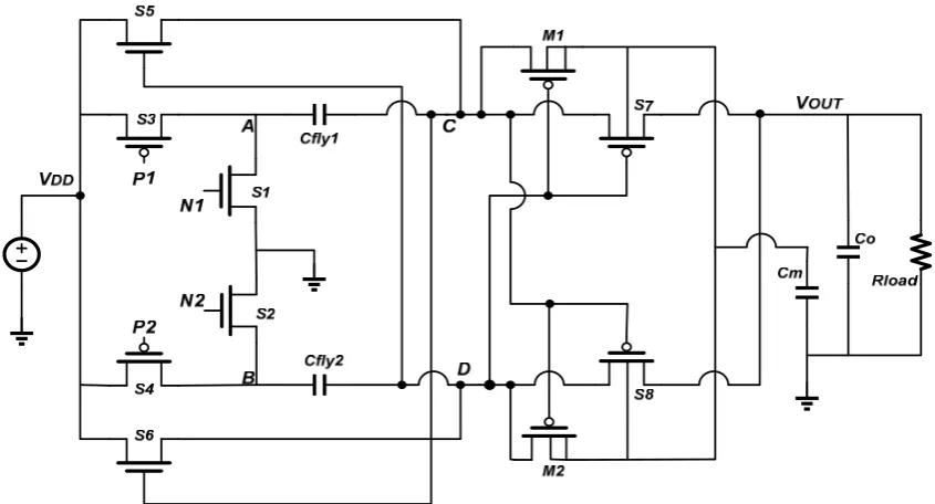
2.3 Proposed Low Noise, High Efficiency Envelope Modulator Structure……….24
Chapter 3 First Stage High Efficiency Charge Pump Design………...29
3.1 Switching Capacitor Voltage Doubler Structure……….………..29
3.1.1 Operating Principle……….30
3.1.2 Non-Overlapping Clock Design………32
3.2 Efficiency Calculation………33
vi
3.2.2 Dynamic Power Loss………35
3.3 Design Flow………38
3.4 Parameter Selection and Efficiency Optimization………...39
3.5 Simulation Results and Summary………43
Chapter 4 Second Stage Adaptive Buck Converter Design and System Simulation Results………45
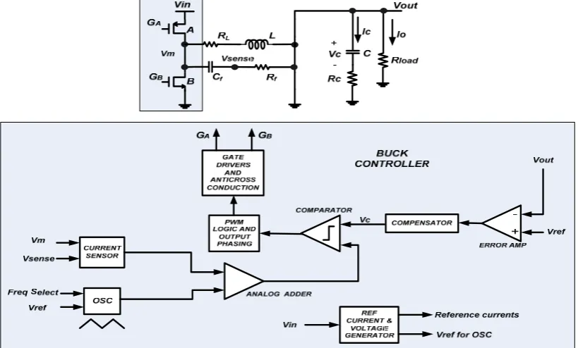
4.1 Circuits Topology and Operation………...46
4.2 Power Stage Design………...48
4.3 Controller Design………..50
4.3.1 Current Sensing Circuits……….52
4.3.2 Compensator Design………...54
4.4 Ripple Cancellation Circuits Design………..57
4.5 Efficiency Optimization………59
4.6 System Simulation Results and Summary………...64
Chapter 5 Alternative Two Stage Solutions………69
5.1 Regulated Voltage Doubler Followed by Buck Converter………69
5.2 Regulated Voltage Doubler Followed by Linear Regulator………..71
5.3 Boost Converter Followed by Buck Converter………..72
5.4 Structure Comparison………74
Chapter 6 Conclusion and Future Work……….75
6.1 Summary………75
6.2 Limitations……….75
6.3 Future Works……….79
vii
LIST OF FIGURES
Figure 1.1 Position of the EDGE system between other wireless standards……….3
Figure 1.2 EDGE signals in time and frequency domains……….4
Figure 1.3 Block diagram of a direct-conversion transmitter………4
Figure 1.4 Adjacent channel power ratio………..6
Figure 1.5 Illustration of error vector in the I/Q plane……….6
Figure 1.6 Linear PA structure……….8
Figure 1.7 Bias points for linear PAs………9
Figure 1.8 Schematic of the polar modulation for a nonlinear RF PA………12
Figure 1.9 Schematic of envelope tracking method………14
Figure 2.1 Schematic of a linear regulator………..21
Figure 2.2 Schematic of a step down switching regulator………..22
Figure 2.3 Schematic of a voltage doubler……….24
Figure 2.4 Schematic of 4SBBC……….25
Figure 2.5 Spectrum simulation results for 4SBBC………26
Figure 2.6 Proposed two stage envelope modulator structure……….27
Figure 3.1 Voltage doubler structure………...30
Figure 3.2 Cross section and equivalent schematic of the PMOS in n-well process………...31
Figure 3.3 Non-overlapping clock generator………...32
Figure 3.4 Simulation waveforms of the driver signals………...33
Figure 3.5 Equivalent modeling of voltage doubler………34
Figure 3.6 Charging a capacitor through a PMOS transistor………..35
Figure 3.7 Switch power losses versus gate width……….37
Figure 3.8 Design flow of voltage doubler……….38
Figure 3.9 Time domain voltage probability statistic chart of EDGE signal………..40
Figure 3.10 Efficiency versus flying capacitance value………..41
Figure 3.11 Contour graph of efficiency versus switch width……….42
Figure 3.12 Efficiency versus load current………..43
Figure 4.1 Schematic of synchronous buck converter……….46
Figure 4.2 Steady state waveforms of buck converter……….47
Figure 4.3 Schematic of Power Stage………..48
Figure 4.4 The bode plot of the power stage………...50
Figure 4.5 The block diagrams of the current mode buck controller………..51
Figure 4.6 The block diagram of AFA……….53
Figure 4.7 Schematic of Analog Adder Using AFA Structure………54
Figure 4.8 Control diagram from the EDGE reference input to output………54
Figure 4.9 One zero two pole compensator………55
Figure 4.10 The bode plot of the compensator………..56
Figure 4.11 The bode plot of the open loop and close loop transfer function………56
Figure 4.12 Ripple cancellation circuits and key waveforms………..57
Figure 4.13 Buck converter ripple voltage versus load current………...59
viii
Figure 4.15 Simulation results of efficiency versus time………62
Figure 4.16 Energy efficiency versus main switch PMOS width………63
Figure 4.17 Time domain simulation results………...64
Figure 4.18 Test bench for simulating the spectral performance……….65
Figure 4.19 Spectrum simulation results of the proposed two stage structure………66
Figure 4.20 Effects of delay mismatch in spectral performance……….67
Figure 5.1 Schematic of the regulated charge pump………70
Figure 5.2 Spectrum simulation results of regulated charge pump………71
Figure 5.3 Spectrum simulation results of boost followed by buck………73
Figure 6.1 Cross section of a NMOS transistor………..……….76
Figure 6.2 Voltage doubler structure………...77
ix
LIST OF TABLES
Table 1.1 Summary of various wireless communication standards………...2
Table 1.2 Performance summaries of different PAs………10
Table 2.1 Comparison of different dynamic power supply methods………...16
Table 2.2 Summary of previous researches on dynamic supply of PAs………..17
Table 3.1 Summary of the voltage doubler parameters………...43
Table 4.1 Summary of power losses in the adaptive buck converter………..60
Table 4.2 Design Parameters of Buck converter……….64
Table 4.3 Summary of spectral performance for different structures……….68
Table 5.1 Summary of various two stage solutions………74
1
Chapter 1 Introduction
Nowadays, wireless communication and mobile systems play an important role in our
daily life. Cellular telephones, personal digital assistants (PDAs), satellite television, global
positioning systems (GPS), and other wireless networking devices have changed our way of
living tremendously. As predicted by Moore’s law [Moore’65], the transistor count in a
single chip will double every eighteen months and the performance of integrated circuits (ICs)
will increase while the cost will go down, which in turn makes it possible to integrate more
functions in a single mobile device. However, the main drawback in device shrinking is
increased power consumption. For wireless handheld devices and other portable applications,
minimizing power consumption is especially crucial to prolong the battery life. This issue is
partly solved by the development of semiconductor processing and battery technology,
however there is still much room for innovation in wireless transmitter architecture and
integrated circuits design.
1.1
Wireless Communication Standard
1.1.1 The evolution of 2G and 3G standard
Table 1.1 summarizes the specifications of different wireless standards. Thanks to the
agreement that led to the development of the Global System for Mobile Communications
(GSM) standard twenty years ago, the mobile telephony market has been growing rapidly
ever since. Today, the GSM family makes up 85% of the global mobile services market and
2
Table 1.1 Summary of various wireless communication standards [McCune’05]
As shown in Table 1.1, the third generation (3G) wireless systems such as
CDMA2000 and Wideband CDMA offer a significant increase in channel capacity and are
suited for broadband data access [Steer’07]. However a higher data transmit rate requires
more signal bandwidth and a higher power control dynamic range. The high data rate means
larger amplitude modulation of the signal in order to increase the number of bits per
transmitted symbol, which in turn results in a larger peak to average ratio (PAR) of the
modulated signal. Thus the efficiency of the power amplifier (PA) will decrease due to
increased power back-off [Lee’04]. Additionally, more signal bandwidth means the change
of the symbols happens at a faster rate, which results in more stringent design specifications
3
1.1.2 Enhanced Data rate for GSM Evolution (EDGE) Standard
EDGE standard is known as a transition from 2G to 3G network and it is compatible
with the GSM standard. Fig. 1.1 illustrates the comparison of the EDGE standard and other
wireless standards in terms of transmit range and bit rate. The development of the EDGE
standard stems from the urgent need for increasing the system data transmit capacity within
the same 200 kHz GSM bandwidth, so it is necessary to use an efficient modulation
technique that can provide a higher throughput/occupied bandwidth ratio.
Figure 1.1 Position of the EDGE system between other wireless standards [Reynaert’06]
The time and frequency domain EDGE signals are shown in Fig. 1.2. The modulation
scheme for EDGE is 3 / 8π offset 8-phase-shift-keying (8PSK). Since one symbol now
contains 3 bits of information, the data rate is 812.5 kbps, 3 times faster than that of the GSM
standard, which uses Gaussian-minimal-shift-keying (GMSK). The main difference between
these two modulation methods is that GMSK has constant envelope signal, while both the
envelope and the phase signal are changing for 3 / 8π offset 8PSK modulation
4
Figure 1.2 EDGE signals in time and frequency domains
1.2
Power Amplifiers (PAs) in Wireless Transmitter
Wireless portable devices require a radio frequency (RF) transmitter to send the
information signal to the nearest base station. Fig. 1.3 shows a simple block diagram for a
direct-conversion transmitter.
Figure 1.3 Block diagram of a direct-conversion transmitter
As shown in Fig 1.3, the PA is the last stage of the transmitter and serves as the
interface between the baseband modulated signal and the antenna. The goal of the PA is to
provide enough power to drive the antenna so that the electromagnetic signal it transmits can
5
distortion in order to prevent spectrum regrowth both inside and outside its bandwidth (i.e.
interfering with other channels), which means the PA should have very high linearity. On the
other hand, as the PA is the most power consuming block in the transmitter, high efficiency
is highly desirable for prolonging the battery life.
Besides linearity and efficiency, other keywords used to define the performance of
the PA are output power and gain. Generally speaking, output power and linearity are set by
the wireless standard, and if they are not met the PA is considered useless. Efficiency and
gain are both related to the battery lifetime, a high efficiency and high gain PA consumes less
battery power [Reynaert’06]. These four parameters are related to each other and it is
difficult to optimize all of them simultaneously. The most common issue is the PA linearity
and efficiency tradeoff, which will be illustrated in the rest of this section.
1.2.1 PA Linearity
Linearity of the PA is measured both in-band and out-of-band, and the specifications
related to the measurement are discussed as follows:
(a) Adjacent Channel Power Ratio (ACPR):
ACPR is the performance metric that measures how much of the signal is spreading
into the adjacent channel as the result of the nonlinearities of the PA. In Fig. 1.4, ACPR is
defined as the power contained in a defined bandwidth (BW2) at a defined offset ( fO) from
the channel center frequency ( fC), divided by the power in a defined bandwidth (BW1)
6
Figure 1.4 Adjacent channel power ratio
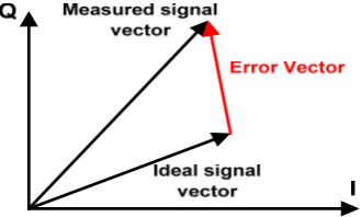
(b) Error Vector Magnitude (EVM):
In digital communications, the digital bits signal is modulated onto an analog carrier
by changing its magnitude and phase, and they can be mapped as the specific locations on in
phase (I) and quadrature-phase (Q) planes, which commonly known as the constellation
diagram. The EVM is defined as the scalar distance between the end points of measured
signals and reference signals, as shown in Fig. 1.5.
Figure 1.5 Illustration of error vector in the I/Q plane
The error vector is a complex parameter which contains both magnitude and phase
information, EVM is measured as the root mean square (RMS) value of the error vector and
7
1.2.2 PA Efficiency
The efficiency of the PA is defined in different ways, the most straightforward
definition of which is drain efficiency:
out Drain
DC
P P
η = (1.1)
where Pout is the output power and PDC is the power drawn from the DC supply.
Another definition is power added efficiency (PAE), which includes the losses due to
the input power and is defined as:
out in PAE
DC
P P
P
η = − (1.2)
PAE takes the gain of the PA into consideration and therefore describes the performance of
the PA more accurately than drain efficiency. PAE can be rewrite as:
(1 1/( / ))
in
out out
PAE
DC
P P P
P
η = − (1.3)
PAE approaches drain efficiency as the power gain /
in
out
P P goes to infinity.
Drain efficiency and PAE represent the performance of the PA only when it works at
the peak output power. In EDGE and other wireless communication standards, the PA
operates at its peak power only for a little fraction of time, while most of the time the PA
operates at 20dB to 30dB power backoff. The average efficiency of the PA, which takes the
output power’s probability density function (PDF) in to consideration, is the most important
measure in determining the battery life for the transmitter [Sevic’97]. The average efficiency
is defined as:
( )
( )
L L L
a v g
S U P P L Y L L
P g P d P
P g P d P
8
where PL is the instant power delivered to the load, PSUPPLY is the instant power drawn from
the DC supply, and (g PL)is the probability density function of wireless standard. ηavg shows
to what extent the PA converts battery power to transmitted power.
1.2.3 PA Classification
Power amplifiers are traditionally divided in several classes based on the different
driving schemes and the harmonic content of the drain voltage. In wireless communication
systems, the most important classification is linear class PA such as class A, B and AB, and
nonlinear class PA which contains class C, D, E and F [Lee-1’04].
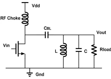
(a) Linear Classes:
Figure 1.6 Linear PA structure
Linear class PAs are usually differentiated by the conduction angle of the transistors.
Fig. 1.6 represents the typical structure of all the linear PAs. The RF choke inductor feeds
DC power to the drain. The drain is connected to a tank circuit through the DC block
capacitor to prevent any DC dissipation to the load.
Fig. 1.7 shows the DC bias points for different linear PAs. The straightforward
9
nonzero, which means reducing the conduction angle. A class B PA is typically biased at the
threshold of the transistor so the conduction angle is 180 degree, and the maximum
efficiency is increased to 78%, with the sacrifice of linearity. The conduction angle and
efficiency of a class AB PA sits between those of class A and class B.
VDS
ID
VDS-SAT
ID-max
QA
QAB
QB
VGS5
VGS4
VGS3
VGS2
VGS1
0
Figure 1.7 Bias points for linear PAs
(b) Nonlinear Classes:
The nonlinear PAs use different schemes to maximize the efficiency. The structure of
a class C PA is the same as its linear counterparts but it is biased at a conduction angle of less
than 180 degrees, which results in deterioration of amplitude linearity but improvement of
efficiency. The maximum efficiency of class C PA approaches 100% as the conduction angle
approaches zero degree.
Class D and class E PAs are known as switching PAs. They are different from linear
PAs in that the transistors are driven hard enough to make them act like switches, and
therefore theoretically there will be no time that the current and the voltage are both nonzero,
ideally resulting in 100% efficiency. A class D PA usually uses two active elements to create
a square wave and then it is filtered by a high Q tank structure, while a class E PA uses a
high-order reactive network that provides enough freedom to shape the switch voltage to
10
A class F PA increases its frequency by using a quarter wavelength of transmission
line or resonant band-stop filter. By cleverly arranging for the square-wave voltage to see no
load at all frequencies above the fundamental, the switch current is ideally zero both at
switch turn on and turn off times, leading to 100% maximum efficiency.
The summary of the different PAs are listed at Table 1.2.
Table1.2 Performance summaries of different PAs
Class I-V Waveform Efficiency ηMAX %
Conduction Angleφ A 2 2 2 OUT DD V V
η= 50% 3600
B 4 OUT DD V V π
η= 78.5% 1800
AB
sin
4(sin cos )
2 2 2
OUT DD V V φ φ η= φ φ− φ −
50%-78.5% 180
0-3600
C
sin
4(sin cos )
2 2 2
OUT DD V V φ φ η = φ φ− φ
− 100% <1800
D / 100% <1800
E / 100% <1800
11
1.2.4 Linearity and Efficiency Tradeoff
The most important factor to increase the battery lifetime in portable devices, such as
mobile phones for EDGE communication, is to minimize the power drawn from the battery
to the power-hungry PA, and meet the wireless communication standard linearity
specification at the same time. However, the linearity and efficiency tradeoff discussed in the
preceding chapter makes it difficult to realize a high linearity and energy-efficiency PA for
portable application. Linear class PAs have high linearity but the efficiency is low. Nonlinear
class PAs can ideally achieve 100% efficiency, but may result in severe signal distortion
between the input signal and output signal. Nowadays numerous PA linearization and
efficiency boosting techniques are used in order to solve this problem. The scheme for
designing an efficient, high linearity PA can be divided into two categories: (a) improve the
linearity of a non-linear PA and (b) improve the efficiency of a linear PA. Both methods will
be discussed in the following section.
1.3
PA Linearization Techniques
Linearization techniques basically refer to the methods used to improve the linearity
of the PA with additional circuits. The most straightforward and simplest way is to use
negative feedback which is commonly used in low frequency analog circuits design.
However, directly feeding back the output signal from the PA is not practical within the RF
and microwave frequency range due to stability and time causality conflicts [Cripps’99].
12
polar loop feedback and Cartesian loop feedback. Detailed discussions of each scheme can be
found in [Sahu’04] and [Kenington’00].
Different from feedback methods, open loop methods are relatively simple and there
are no bandwidth reduction or stability issues. Several methods such as feedforward,
pre-distortion and linear amplification with non-linear components (LINC) are based on the open
loop operation, but they are seldom used today due to various drawbacks [Lee-1’04].
Today a popular scheme for PA linearization is polar modulation. The idea originates
from the envelope elimination and restoration (EER) technique first proposed by Kahn in
1952 [Kahn’52].
Baseband symbols I/Q to A/P conve
rsion
Figure 1.8 Schematic of polar modulation for a nonlinear RF PA
Fig. 1.8 illustrates the schematic of polar modulation. The baseband generator, which
is often realized by digital signal processing (DSP) circuits, generates the in-phase signal
( )
I t and quadrature-phase signal ( )Q t . The relation between the baseband signals and the RF
signal is give by:
( ) ( ) cos( ) ( ) sin( ) RF
v t =I t ωt +Q t ωt (1.5)
This Cartesian form RF signal is then transferred to polar form, represented by an envelope
13
( ) ( ) cos( ( )) RF
v t =A t ω θt+ t (1.6)
Now the PA is only processing the constant phase modulated signal, so a high efficiency PA
can be used. The time varying envelope signal is then recombined with the phase signal by
dynamically change the supply voltage of the PA through the envelope modulator, which
often realized by a dc-dc converter. The major benefit of the polar modulation is to shift the
linearity requirement from RF to the baseband envelope branch. Many well known
techniques such as feedback can be directly applied at this low baseband frequency to
improve the linearity of the envelope modulator. Moreover, the envelope modulator can be
realized by a high efficiency switch mode power supply. Thus, an efficient high linearity PA
can be achieved by using polar modulation.
The bandwidth of the RF signal depends on the wireless standard. For EDGE
standard, the bandwidth is 200kHz, however, the envelope bandwidth is larger than 200kHz.
In order for the envelope signal to pass through the envelope modulator, a large bandwidth
and a high switching frequency are necessary, if the envelope modulator is realized by a
switch mode power supply. This, in turn, degrades its light load efficiency. Moreover, delay
mismatch of the phase and envelope branch should be compensated to avoid distortion
[Reynaert’06].
1.4
PA Efficiency Boosting Techniques
Linear PA’s efficiency is improved by adjusting the quiescent power consumption
according to the output power, which is achieved by dynamically changing the supply
14
tracking. As shown in Fig. 1.9, in order to adjust the power supply efficiently and rapidly, a
fast switching mode power supply is necessary.
Figure 1.9 Schematic of envelope tracking method
Envelope tracking follows the PA’s instantaneous output power, and therefore it can
achieve high peak power efficiency. However in a wireless transmission system, because the
PA works at power backoff most of the time, the average efficiency is of more concern than
the peak power efficiency. Average power tracking method takes this into consideration, and
it is similar to envelop tracking except that the power supply tracks the average transmitted
power. It provides increased average efficiency for systems with large power control ranges
and low peak to average power ratios.
1.5 Object and Thesis Outline
The objective of this work is to design an envelope modulator for EDGE polar
modulation. The envelope modulator serves as the dynamic power supply for a class E
nonlinear PA, therefore the efficiency should be maximized while the linearity should meet
the EDGE spectral specification.
The thesis is composed of six chapters and is organized as follows: Chapter 1 is the
15
systems is stressed. The PA's linearity-efficiency tradeoff is discussed and some solutions are
provided.
In chapter 2, several existing envelope modulator structures are reviewed in terms of
their performance based on efficiency, noise and cost. The two stage solution is proposed
based on the input and output voltage requirement of EDGE standard.
In chapter 3, the first stage high efficiency voltage doubler design is introduced and
analyzed.
Chapter 4 introduces the implementation of the second stage 10MHz current mode
buck converter. Efficiency optimization and system simulation results are demonstrated.
Chapter 5 discusses the comparison of different two stage structures. Finally the
16
Chapter 2 Literature Review of Dynamic Power Supply
Techniques and Proposed Two Stage Modulator Structure
As discussed in the chapter 1, dynamic power supply techniques can improve the
efficiency of the linear PA and the linearity of the nonlinear PA. A summary of
state-of-the-art dynamic power supply techniques highlighting their key advantages and disadvantages is
presented in Table2.1.
Table2.1 Comparison of different dynamic power supply methods
Method Advantages Disadvantages
Envelope Tracking High peak power efficiency
High switching frequency for DC/DC converter. Requirement for delay
mismatch
Average Envelope
Tracking Increase average efficiency Low peak power efficiency
Polar Modulation
/EER High peak power efficiency
High switching frequency for DC/DC converter. Requirement for delay
mismatch
Numerous publications have addressed dynamic power supply techniques in recent
years. Section 2.1 serves as the literature review of current dynamic power supply methods.
Different switch mode power supply structures are compared in terms of efficiency,
complexity and spectral performance in section 2.2. The proposed two stage structure suited
for EDGE polar modulation is introduced at the end of this chapter.
2.1 Literature Review of Previous Work
Table 2.2 highlights publications that are representative of previous research in the
17
applications in terms of structures, switching frequencies and efficiencies. It is important to
note the difference between the maximum efficiency and the average efficiency, the former
parameter is only specified at maximum output power and therefore may not directly related
to the battery life, as discussed by Sevic [Sevic’97]. It is the average energy efficiency, which
takes the PDF of transmitted signal into consideration, determines the battery performance in
the RF transmitter.
Table2.2 Summary of previous researches on dynamic supply of PAs * PA and envelope modulator
** Envelope modulator only
Method Author Modulator
Type Application
Envelope Bandwidth Switching Frequency Max Efficiency Average
Efficiency Reference
Envelope Tracking
Midya,etc
(Motorola) Buck QPSK 160kHz 800kHz 90%** [Midya’01]
Schlumpf,etc
(EPFL) Buck IS95-CDMA 1.5MHz 16MHz 85%**@95mA [Schlumpf’04]
Wang, etc
(UCSD) Hybrid Buck OFDM 20MHz 100MHz 30%*@0.1W [Wang-1’05]
Hanington,etc
(UCSD) Boost IS95-CDMA 1.22MHz 10MHz
65%**@0.2W
74%**@1W 6.38%* [Hanington’99]
Average Envelope Tracking
Staudinger,etc
(Motorola) Buck
IS95B-CDMA 500kHz 5MHz 90%** 11.4%* [Staudinger’00]
Sahu, etc
(Georgia Tech) Buck-Boost IS95-CDMA 1.5MHz 500kHz
10%**@LL
65%**@HL 6.78%* [Sahu’04]
Polar Modulation/EER
Su, etc (Hewlett-Packard Lab)
Delta NADC 49%*@1W [Su’98]
Nagle, etc (M/A-COM
Eurotec)
Interleaving
Delta 800kHz 80%** [Nagle’05]
Wang, etc (UC
Boulder) Buck 12kHz 200kHz 60%* 96%** [Wang-2’04]
Jiang, etc
(UC Boulder) Buck EDGE 1MHz 4.3MHz [Jiang’06]
Jinseok, etc
18
2.1.1 Envelope Tracking
As discussed in section 1.3, the supply voltage of the PA is dynamically changed
according to the output power level in an envelope tracking system. As a result, the PA
operates at high efficiency even in the power backoff range.
Midya from Motorola described a buck envelope modulator used for a 25 kHz QPSK
signal [Midya’01]. Sensorless current mode control is used and the buck converter can
achieve a maximum efficiency of 90% at the switching frequency of 800 kHz. The efficiency
of the whole transmitter is about 50% at 20W peak RF power. This is twice as efficient as
using a constant power supply class AB PA.
Schlumpf proposed a buck converter used for CDMA application [Schlumpf’04]. Its
switching frequency is 16MHz, which makes it capable of tracking the 1.5MHz envelope
bandwidth, and the efficiency of the modulator is 85% at an output voltage of 1.25V and a
load current of 95mA. Simple hysteretic control is used.
In [Hanington’99], a boost dc-dc converter with an operating frequency of 10MHz
was demonstrated using a GaAs HBT, which can boost the power supply of PA to between
3V and 10V when the output power is larger than 18dBm. The efficiency of the converter is
in the range of 65%-74% for output powers in the range of 0.2-1W. The overall average
efficiency of the transmitter was reported as 6.38% for dynamic power supply, compared to
3.89% for a 10V power supply PA.
Wang proposed a hybrid buck converter for an envelope tracking PA used for a
WLAN802.11g application [Wang-1’05]. With the combination of a linear regulator and a
19
20MHz. The overall system peak drain efficiency was reported as 30% at the output power of
0.1W.
2.1.2 Average Envelope Tracking
An average envelope tracking method increases the average efficiency by tracking the
RMS value of the output power level. Staudinger from Motorola introduced a buck converter
that serves as an envelope modulator for a CDMA application [Staudinger’00]. Working at a
5MHz switching frequency, the converter can achieve 90% peak efficiency. The system
average efficiency is increased from 2.2% to 11% by changing the PA's supply voltage.
Sahu from Georgia Institute of Technology proposed a buck-boost average envelope
tracking modulator for a CDMA application [Sahu’04]. The switching frequency of the
converter is 500 kHz with an efficiency of 10%-65% over 0.4V-4V output. The overall
system average efficiency is improved to 6.78%, which is 4 times better than the fixed supply
efficiency.
2.1.3 Polar Modulation/EER
Polar modulation/EER can be done by amplitude modulating the supply voltage of a
nonlinear PA through an envelope modulator. In [Su’98] and [Nagle’05], the envelope
modulator uses delta modulation. The paper written by Su claimed the maximum efficiency
of the transmitter is 30% at the output power of 1W. Nagle proposed the interleaving delta
modulation method and enables the envelope modulator to achieve a maximum efficiency of
20
Wang from the University of Colorado at Boulder demonstrated the design of a 10
GHz drain modulated class E PA using a buck converter as the envelope modulator
[Wang-2’04]. The switching frequency of the buck converter is only 200 kHz and 96% peak
efficiency can be achieved, the peak efficiency of the whole system is reported as 60%.
In 2006, Jiang proposed a buck envelope tracker for a Polar EDGE transmitter
[Jiang’06], which switches at 4.33 MHz with the capability of tracking 1.3 MHz of envelope
bandwidth. The controller design for the buck converter produces an overall Bessel type
low-pass transfer function, which gives a constant time delay for the envelope modulator.
However, the efficiency of the converter is not reported.
An envelope tracker for EDGE polar modulation is also addressed in Jinseok’s paper
[Jinseok’08], A 10MHz 4 switch buck boost converter (4SBBC) is used, which uses current
mode control. The average efficiency for the converter is 82% when the input battery
voltage is 3.3V and the output voltage changes from 0.7V to 5V based on the EDGE standard.
2.2 Switch Mode Power Supply Circuits Structure
The envelope modulator realized by the dc-dc converter is the most important block
of the RF transmitter, which transforms a fixed battery supply into different voltage levels for
dynamic supply of a PA. Different envelope modulator structures are discussed in the
preceding section. For battery powered systems and wireless application, the important
specifications for the dc-dc converters are high efficiency, low cost and low spurious noise.
Switch mode dc-dc converters can be divided into three categories: linear regulator,
21 (a) Linear Regulator
Figure 2.1 Schematic of a linear regulator
Fig. 2.1 illustrates the schematic diagram of linear regulator. The passive transistor
(PMOS in the graph) operates in the saturation region and connects between the input and the
output. An error amplifier is used in the negative feedback loop to ensure that the output
voltage is equal to the control voltage, which in turn is usually generated by bandgap
reference circuits. By controlling the voltage drop across the passive transistor, the output
voltage can be regulated regardless of change in the input voltage or load current. When the
output voltage is regulated to a voltage very close to the input voltage, the regulator is said to
work in dropout mode and the transistor is forced to work in the linear region.
The power loss of the linear regulator depends on the load condition and voltage ratio.
Specifically, the efficiency can be calculated as:
%
( )
OUT LOAD OUT
IN OUT LOAD OUT LOAD IN
V I V
V V I V I V
η =
− + (2.1)
[Rincon-Mora’02]. So a linear regulator can only achieve high efficiency in the region where
the input and output voltage are close, which is not well suited for a dynamic power supply
22
Although linear regulator is easy to design, the abovementioned drawbacks limit its
application.
(b) Switching Regulator
A switching regulator is the most commonly used structure in dc-dc converter design.
Its merit lies in the fact that for a fixed input voltage, both efficient up (boost) and
step-down (buck) voltage conversion can be achieved. Fig. 2.2 shows the synchronous buck
converter for lowering the input voltage. The gate voltages of the transistors are controlled so
that they are “on” and “off” respectively, and as the result, the input voltage is chopped at the
summing node. An inductor and a capacitor form a low pass filter. The output voltage is the
average of the chopped voltage, which is fed back to an error amplifier and control circuits to
generate the correct pulse width to control the transistor. This is called pulse width
modulation (PWM) and the feedback scheme is used to ensure the regulation of the output
voltage [Ericsson’02].
23
Theoretically the efficiency of the switching regulator is 100% because the inductor
and capacitor do not consume power, and the voltage and current do not both cross the
transistor at the same time. However, there will be a short V-I overlap in reality which will
dissipate power. Also the inductor and capacitor’s parasitic resistances will consume some
power. Even taking all the parasitics into consideration, the switching regulator can still
achieve very good efficiency. The output voltage is not constant and there will be a
switching ripple at the output, which in turn generates some noise in the spectrum domain,
for a switching regulator used in a dynamic power supply system, methods should be taken to
ensure that the output ripple noise does not exceed the spectrum mask for the required
specifications.
(c)Switching Capacitor Circuits
Switching capacitor circuits, also known as charge pumps, are well suited for
battery-powered applications since there are no inductors in the structure, only external capacitor are
required for voltage conversion, and therefore they are compact and low cost, they also have
spectral performance superior to that of the switching regulators [Maxim].
Fig. 2.3 shows the schematic of a simple voltage doubler. The switches are controlled
in such a way that S1 and S2 first turn on half of the period. The flying capacitor connects in
parallel with the input and it is charged to a voltage equal to the input voltage. Then S3 and
S4 turn on while S1 and S2 turn off for the rest of the period. Since the voltage drop across
the flying capacitor cannot change instantly, it connects in series with the input so that twice
24
Figure 2.3 Schematic of a voltage doubler
The efficiency of a charge pump is ideally 100%. However, when charging and
discharging the capacitor C, there will be energy loss in each switching cycle as:
2
(1/ 2) LOSS
E = C VΔ (2.2)
The conduction loss due to the equivalent resistors of the switches will also decrease the
overall efficiency.
From the above analysis, switching regulators and the charge pumps are the suitable
candidates for dynamic power supply of PAs.
2.3 Proposed Low Noise, High Efficiency Envelope Modulator Structure
for EDGE Polar Modulation
The PA serves as the load for a dc-dc converter envelope modulator. A class E PA
can be modeled as a constant resistor [Sokal’75]. Based on the EDGE output power
requirement and the specification of a 17dB PAR [3GPP’05], the output voltage of the
envelope modulator changes from 0.7V to 5V. The input voltage of the envelope modulator
is connected to the battery. A lithium-ion battery is typically used, as it has a higher energy
25
charged and 2.7V when fully discharged, with a nominal operating voltage of 3.3V [NSC].
Due to the input and output voltage requirements of the envelope modulator, both step-down
and step-up voltage conversions are needed.
Another feature of the EDGE signal can be revealed by its frequency domain
information. As shown in Fig. 1.1, the complex EDGE signal has the most energy within the
bandwidth of 200 KHz. However, the bandwidth of the envelope has a wider spectrum. The
bandwidth needed for the envelope modulator is 1-2MHz [Jinseok’08], which means the
switching frequency should be much higher.
In recent years, numerous papers address dynamic power supply design for EDGE
polar modulation. Many of the polar transmitters still use low dropout (LDO) linear
regulators to realize the modulators for simplicity, resulting in low average energy efficiency.
Others use switching regulators but have other drawbacks. In [Jiang’06], the battery voltage
is fixed at 3.6V, and therefore the envelope modulator cannot make full use of the battery
voltage range. Jinseok takes the characteristics of the battery into consideration and proposes
a 4SBBC structure for realizing the envelope modulator. As shown in Fig. 2.4 [Jinseok’08],
four switches are controlled to give the step down or step up functions based on the
requirement.
26
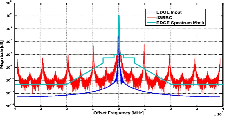
Fig. 2.5 illustrates the spectrum simulation results of the 4SBBC structure. Although
the average efficiency is good and the in band spectrum meets the EDGE standard, the
out-of-band spurious noise exceeds the EDGE spectrum mask at the switching frequency of
10MHz and its harmonics.
-4 -3 -2 -1 0 1 2 3 4
x 107 10-14 10-12 10-10 10-8 10-6 10-4 10-2 100 102
Offset Frequency [MHz]
M a gni tude [ d B ] EDGE Input 4SBBC
EDGE Spectrum Mask
Figure 2.5 Spectrum simulation results for 4SBBC (Courtesy of Jinseok Park)
Most of the switching spurious noise is generated when the 4SBBC works in the
step-up (boost) region. Here the inductor is connected to the input and all the current flows to the
output to charge the output capacitor, which in turn generates large ripple voltage at the
output, resulting in spectral performance deterioration. The same problem does not occur
when 4SBBC works in the step-down (buck) region, where the inductor is connected to the
output and only inductor ripple current follows to the output capacitor. The noise
performance in this case is much better than the boost case.
From the above analysis, if we can get rid of the high noise boost region of the
27
and the EDGE specifications can be met. The proposed two stage structure is based on this
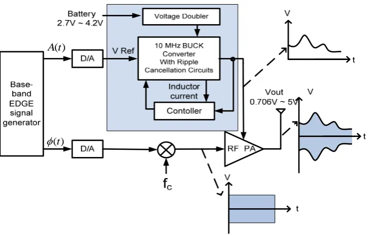
idea. Fig. 2.6 shows the proposed envelope modulator structure for EDGE polar modulation.
Instead of using 4SBBC, a high efficiency charge pump is used as the first stage to boost up
the battery voltage, and then a buck converter is used as the second stage to step down the
voltage based on the EDGE output specification.
)
(t
A
)
(t
φ
Figure 2.6 Proposed two stage envelope modulator structure
Compared to a linear regulator, a buck converter is more energy efficient for the
dynamic output voltage applications, and high overall efficiency is achieved if a high
efficiency charge pump is used as the first stage to boost the voltage. On the other hand, a
buck converter has better spectrum performance than the buck-boost counterpart. In order to
further reduce the noise, ripple cancellation circuits are added to the buck converter. The
detailed design of the proposed two stage envelope modulator will be discussed in the
28
first stage, and chapter 4 discusses the implementation of the buck converter, as well as the
29
Chapter 3 First Stage High Efficiency Charge Pump Design
As discussed in the preceding chapters, the input voltage for envelope modulator is
set by the Li-ion battery as from 2.7V to 4.2V, and the output voltage is changing between
0.7V to 5V determined by the EDGE standard. Although buck-boost converter seems to be a
good candidate for this application, the output spectrum cannot meet the EDGE requirement
[Jinseok’08], and therefore charge pump circuits followed by a buck converter is proposed.
In this two stage envelope modulator design, the role of the charge pump circuits is to
boosting the battery voltage to higher level so that only step down conversion is necessary in
the second stage. For the worst case condition, the 2.7V input voltage should be boosted to
above the maximum output voltage 5V so as to make full use of the battery, as the result,
voltage doubler is a possible solution for this condition. High efficiency is crucial for charge
pump design, and since the output of the charge pump is connected to the input of the buck
converter, the ripple generated by charge pump will propagate to the second buck stage,
therefore low ripple voltage at the output is preferred.
The voltage doubler structure and its working principle will be discussed in section
3.1, followed by the loss and efficiency calculation, parameter selection and efficiency
optimization. Simulation results will be demonstrated at the end of this chapter.
3.1 Switching Capacitor Voltage Doubler Structure
In recent years, voltage doublers are widely used in battery-powered portable
applications, such as provide a higher supply voltage for driving the light emitting diodes
30
voltage doubler is the most commonly used topology. Fig. 3.1 shows the schematics of the
cross-coupled voltage doubler [Favrat’98].
Figure 3.1 Voltage doubler structure
3.1.1 Operating Principle
As shown in Fig. 3.1, the voltage doubler can be considered as two identical branches,
one branch consists of switch S1, S3, S5 and S7, auxiliary switch M1 and flying
capacitorCFLY1, the rest of the switches and CFLY2 are belong to another branch. Both
branches share the same input voltage from the Li-ion battery, and the same output capacitor
and load. The gate of switch S5 and S6, S7 and S8 are cross-coupled, which eliminates the
need for separate bootstrap gate drivers.
The operation of the voltage doubler can be illustrated as follows: P1 and N1, P2 and
N2 are connected to clock drive signals changing from 0 toVDD with the duty cycle of 50%,
31
so that the voltage at node B isVDD, since CFLY2was charged to VDD in the previous half cycle
and the voltage across the capacitor cannot change abruptly, the voltage at node D will be
pumped to 2VDD. On the other hand, S1 is on and node A is approximately at zero voltage,
since the gate of S5 is connected to node D which is 2VDD, S5 will also on and the capacitor
1 FLY
C will be charged to VDD through S5 and S1. On the other hand, the voltage at node C
and node D is VDD and 2VDD, respectively, switch S8 turns on and the output capacitance is
charged to 2VDD through switch S4 and S8. In another half cycle, the voltage at node C and
node D will be opposite and the output capacitance will also be charged to 2VDD through S3
and S7.
The auxiliary switches M1 and M2 are important in this structure because they can
prevent the bulk of S7 and S8 from switching. For standard n-well CMOS technology, the
cross-section of PMOS in a p-substrate is shown in Fig. 3.2 with its equivalent schematics
[Favrat’98], there are two vertical and one lateral parasitic bipolar transistors exist in this
structure, which results in difficulty for accurately modeling the switches, and if these
parasitic transistors are triggered on, leakage current will flow from drain and source to
ground, which in turn increase the power loss.
32
The only possible solution to get rid of the parasitic transistors is to tie the bulk
terminal at the highest voltage between source and drain, and that is exactly why the
auxiliary switch M1 and M2 are used, they are controlled in such a way so that the bulk of
the main switches S7 and S8 always stay at highest voltage between there sources and drains,
and therefore bulk switching is prevented.
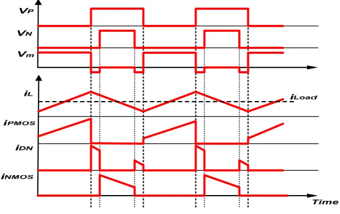
3.1.2 Non-Overlapping Clock Design
For voltage doubler structure shown in Fig.3.1, P1 and N1, P2 and N2 should not be
turned on at the same time, otherwise the short-circuit current will flow from the battery to
ground and increase the power loss. On the other hand, we should also make non-overlapping
drive signals at P1 and P2, N1 and N2 to prevent the discharging current to the ground.
Therefore drive circuits should be carefully designed and non-overlapping clock should be
generated.
Figure 3.3 Non-overlapping clock generator
The schematic of the non-overlapping clock generator is shown on Fig. 3.3.
33
inserted to adjust the dead time and increase the drive capability. The cadence simulation
results in shown in Fig. 3.4 and illustrated its functionality.
(a) Waveforms at P1 and N1, P2 and N2 (b) Waveforms at P1 and P2, N1 and N2 Figure 3.4 Simulation waveforms of the driver signals
3.2 Efficiency Calculation
Unlike the switching regulators, the charge pump circuits usually works at open loop
and fixed frequency [Wang-3’97]. The power loss of the voltage doubler consists of two
parts: resistive power loss which depends on the load currents, ESR of the flying capacitors,
on-resistances of the switches, and dynamic power loss which relates to the switch size,
output voltage and switching frequency. The modeling of voltage doubler and efficiency
calculation method will be discussed in the following section.
3.2.1 Conduction Power Loss
At steady state, the switches are operating in the linear region, if we ignore the
channel length modulation effects, the on-resistance RSof the switch is:
( )
S
ox GS T
L R
C W V V
μ
=
34
Where μ is mobility, Cox is the capacitance per unit area of the gate oxide, W and L
represents the switch width and length, VGS is the gate to source voltage, and VT is the
transistor threshold voltage.
The equivalent resistance RC and ESR of the flying capacitors should also be taken
into consideration, the equation to calculate RC can be written as:
1 2 C
S FLY
R
f C
= (3.2)
The factor 2 comes from the two flying capacitors which act at each phase of the clock cycle
[Favrat’98]. So the total on-resistance RCON for each half clock cycle is:
1 2
2 ( ) ( )
p n
CON C S ESRC ESRC
S FLY n ox n GS n T n p ox p GS p T p
L L
R R R R R
f C μ C W V V μ C W V V
= + + = + + +
− − (3.3)
To simplify the design, the on-resistances of all the switches except the two auxiliary
switches are assumed to be the same and voltage drop across each switch is ignored.
The voltage doubler then can be modeled as the voltage source 2VDD and series
connection of the on-resistance RCON and the load resistanceRLOAD, Fig. 3.5 illustrates the
equivalent modeling of the voltage doubler.
35
The output voltage VOUT and output voltage drop ΔVOUT due to RCONcan be calculated as:
2 LOAD OUT DD LOAD CON R V V R R =
+ (3.4)
2 CON OUT DD LOAD CON R V V R R Δ =
+ (3.5)
3.2.2 Dynamic Power Loss
Dynamic power loss results from charging and discharging the capacitors. For the
charging process, consider a simple circuit in Fig. 3.6, capacitor C is charged by the voltage
source VDD through a PMOS transistor. The energy drawn from the voltage source can be
derived by integrating the instantaneous power over the charging period:
2
0 ( ) 0 0
DD
V OUT
VDD DD DD L DD OUT L DD
dV
E i t V dt V C dt V dV C V
dt
∞ ∞
=
∫
=∫
=∫
= (3.6)The energy stored by the capacitor is:
2
0 0 0
1 ( ) 2 DD V OUT
C OUT L OUT OUT OUT L DD
dV
E i t V dt C V dt V dV C V
dt
∞ ∞
=
∫
=∫
=∫
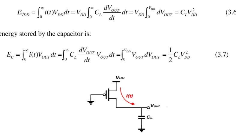
= (3.7)Figure 3.6 Charging a capacitor through a PMOS transistor
From (3.6) and (3.7), we can see half of the energy (1 2
2C VL DD) is lost in the charging process,
during the discharging phase, the stored 1 2
36
so each switching cycle the dynamic loss is C VL DD2 , here VDD is the voltage change across the
capacitor.
The dynamic power loss for the voltage doubler can be calculated in the same way
and all the capacitances should be taken into consideration. Apart from the two flying
capacitors, there are parasitic capacitances at the gate, drain and source of the each switch,
assume the total gate capacitance for each branch is Cg, and the capacitance at node A and C
are CA and CC, respectively. The voltage at these nodes will swing between VDDand 2VDD,
so the voltage change across these parasitic capacitances is equal toVDD. We can define the
total parasitic capacitances CP for each branch as:
P A C g
C =C +C +C (3.8)
P
C is proportional to the gate width Wand gate lengthL. The total dynamic energy loss can
be calculated as:
2 2
2 2
S P DD OUT
E = C V + C VΔ (3.9)
The power efficiency is calculated by the following equation:
% LOAD
LOAD S
E
E E
η =
+ (3.10)
LOAD
E is the energy delivered from the voltage source to the load and is calculated as:
2 OUT LOAD
S LOAD
V E
f R
= (3.11)
37 2 2 1 % ( ) 1 2 2
LOAD CON CON
P S FLY S
LOAD LOAD
R R R
C f C f
R R η = + + + (3.12) CON
R is given by 1
2 ( ) ( )
p n
CON ESRC
S FLY n ox n GS n T n p ox p GS p T p
L L
R R
f C μ C W V V μ C W V V
= + + +
− − (3.3).
From (3.3) and (3.12), the efficiency of the voltage doubler is affected by many
factors, such as switching frequency, output voltage, gate size, load condition and flying
capacitance. There are tradeoffs in selecting these parameters, for example, if the switch
length Lis fixed, increase the switch width Wwill decrease its on-resistance, and in turn
decrease the conduction loss, but the switching loss will increase due to larger parasitic
capacitance.
Figure 3.7 Switch power losses versus gate width
Fig. 3.7 shows the conduction and dynamic loss as the function of the switch width
[Stauth’06], as indicated in the graph, there exist an optimal width of the switch so that the
total loss is at the minimum. Next section will discuss how to select the abovementioned
38
3.3 Design Flow
Figure 3.8 Design flow of voltage doubler
The voltage doubler design process is based on the specification of EDGE system and
semiconductor process information, the goal is to achieve optimum efficiency by using (3.12)
derived in the previous section. Fig. 3.8 illustrates the design flow of the voltage doubler.
The input voltage of the doubler comes from the Li-ion battery and it will decrease
gradually as time goes by, on the other hand, the load condition is also changing based on the
EDGE standard time domain information, which makes it complicate and time consuming to
select the design parameters, many iterations are necessary in order to find the optimum
efficiency. For simplicity, the design and optimization procedure of the voltage doubler is at
the nominal battery voltage and most frequently occurred load condition, and then check and
iterate the design process for the entire load range if necessary. This design procedure will
save lots of time and still get the sub-optimum results.
First of all, input voltage is chosen based on the battery technology, and then we
39
buck converter and the output of buck converter is fast changing EDGE signal, the input
current of the buck converter (also the output load current for voltage doubler) will vary
based on the time domain EDGE information. For simplify the design procedure, we will
find the optimum efficiency at one load condition which occurs most on the PDF of EDGE
standard, then maximize the efficiency for the whole load range.
Secondly, switching frequency and flying capacitor is chosen based on the ripple
voltage requirement, different switch size is selected and equation (3.12) is used to calculate
the efficiency, since there is a tradeoff between the conduction loss and dynamic loss, an
optimum point should be found, and several iteration may be needed to get the optimum size
and efficiency. The detailed parameter selection procedure will be illustrated in the next
section.
3.4 Parameter Selection and Efficiency Optimization
(a) Input voltage and load condition selection
Li-ion battery is used as the input power source for its high power density, the
nominal input voltage is 3.3V [NSC], and therefore the input voltage is picked up as this
voltage.
The output of the voltage doubler is connected to the input of the buck converter,
which is then connected to PA. According to the voltage probability statistic chart of EDGE
standard shown in Fig 3.9, the voltage of EDGE signal is more likely to be located between
2.3 and 4.7V. PA serves as the load of the buck converter and can be modeled as a 5Ω
40
between 1.1W and 4.5W. The doubler should provide the second stage buck converter with
such variable power, as the result, the load current of doubler is changing between 0 and 1A.
In the efficiency optimization procedure, we select the load for the doubler in this range.
Figure 3.9: Time domain voltage probability statistic chart of EDGE signal
(b) Switching frequency and capacitor selection
Next step is to select the switching frequency. For this parallel, opposite-phase driven
voltage doubler structure, the effective ripple frequency at the output is twice the driver
frequency of the flying capacitors. This voltage ripple will be connected to the input of the
buck converter, in order to reduce the input ripple effects at the output of the buck converter,
the ripple frequency should be selected within the bandwidth of the buck converter, under
this condition the input ripple will be suppressed based on the close-loop transfer function of
the buck converter [Ericsson’01]. The typical bandwidth requirement for envelope modulator
used for EDGE polar modulation is around 1-2MHz [Jinseok’08], and therefore we pick up
1MHz ripple frequency as the starting point, which in turn requires the switching frequency
of the voltage doubler as 500kHz.
0 . 5 1 1 . 5 2 2 . 5 3 3 . 5 4 4 . 5 5
0 5 0 1 0 0 1 5 0 2 0 0 2 5 0 3 0 0 3 5 0
V o lt a g e
N
u
mber
41
The output capacitor is then selected based on the ripple voltage requirement. The
ripple voltage at the output can be calculated as:
2 LOAD ripple
S LOAD
I V
f C
= (3.13)
In order for the ripple voltage stay within 100mV range in the worst load condition, the
output capacitor is chosen to be 6.8μF.
The doubler consists of two anti-phase charge pumps. As we know, the flying
capacitor in the charge pump is used as the voltage source. The dynamic loss on the capacitor
is C VΔ 2in one cycle. If the capacitor is too small, then the charging and discharging process
is fast, which results in a large voltage fluctuation ΔV on capacitor and increase the
switching loss. As the result, parameter sweeping is used to determine the flying capacitor
value in order to minimize the dynamic loss and in turn maximize the efficiency. Fig 3.10
shows the simulation results for the efficiency versus flying capacitance at fS =500kHz and
load current of 0.8A, which is the most occurred situation for EDGE signal, the ideal
switches are used.
42
From the simulation results, the flying capacitance CFLY is chosen as4.7μF.
(c) Switch size selection
The length of all the switches is chosen to be the minimal channel length 0.6 μm
based on the process so as to minimize the parasitic capacitance, and both the width of the
NMOS and PMOS are swept to find the optimum efficiency.
Figure 3.11: Contour graph of efficiency versus switch width
The simulation result shown in Fig.3.11 illustrates the relation between the efficiency
and the switch width. As shown on the contour graph, the optimum PMOS width is 150mm,
and the width for NMOS is 100mm.
For auxiliary switches M1 and M2, since they do not need to pass the high load
current, small width of 1mm is chosen for their width and the length is the minimal length.
43
Table 3.1 Summary of the voltage doubler parameters
Technology JAZZ 0.6um
Input Voltage Range 2.7~4.2V
Switching Frequency 500 kHz
Output Voltage Vo=6.45V@Vdd=3.3V
Output Ripple 60mV@Vdd=3.3V, Iload=0.5A
NMOS Switch Size W=100mm,L=600nm
PMOS Switch Size W=150mm,L=600nm
Load Capacitor 6.8uF
Flying Capacitor 4.7uF
3.5 Simulation Results and Summary
As illustrated in last section, the parameter selection and efficiency optimization is
based on the most frequently occurred load condition, in the real fact the load is changing
based on the EDGE standard, and therefore the different load condition should be checked to
ensure the high efficiency.
The comparison between the efficiency simulation results and calculated results based
on equation (3.13) are shown in Fig.3.12 for different load conditions, the simulation results
matches well with the calculated results. The voltage doubler can achieve around 95%
efficiency under most of the load conditions.
![Table 1.1 Summary of various wireless communication standards [McCune’05]](https://thumb-us.123doks.com/thumbv2/123dok_us/1553618.1190727/12.595.87.527.121.394/table-summary-various-wireless-communication-standards-mccune.webp)