GONSALVES, KIRAN. Memory Design for FFT Processor in 3DIC Technology. (Under the direction of Professor Paul D. Franzon).
Computation of Fast Fourier Transform (FFT) of a sequence is an integral part
for the Synthetic Aperture Radar (SAR). For FFT computations, there are a lot of data
modification operations (multiplication and addition) involved. Typically, a memory (either
on-chip or off-chip) would store the input data packet and output data would also be
written to the same location. This memory would also be used as a scratch pad for storing
intermediate results. As the required resolution of the image increases, the size of the
input data increases. Hence, the number of computations in the butterfly structure of the
FFT increases and this results in numerous data transactions between the memory and the
computation units. Each data access can be expensive in terms of power dissipation and
access time. The power dissipation is proportional to the size of the memory and the access
time is dependent on the electrical proximity of the memory to the processing unit.
Three Dimensional Integrated Circuits (3D IC) enable the tight integration of this
memory with the logic that operates on the memory. Apart from form-factor improvement,
3D IC technology’s main advantage is that it significantly enhances interconnect resources.
Davis et al. in [1] mention that in the best case, if the inter-tier vias are ignored, the average
wire length can be expected to drop by (Ntier)0.5
This structure is advantageous as it reduces the access time and enables quicker
computation of FFT when compared to its two dimensional counterpart. Alternatively,
when run at the same speed, the 3D version can be said to dissipate lower power than the
2D version, owing to smaller interconnect parasitics.
The electrical proximity of the memory enables more interconnections (wider
buses) and as a result, many number of small memories can be interfaced to the processing
elements. This would not be possible in the conventional off-chip structure as the number
of interconnect pins would be a limiting factor due to limitations on pin-outs and Printed
Circuit Board (PCB) routing. This thesis supports the demonstration of memory on logic
(ROM) (for storing twiddle factors for FFT computation). For the application a dual ported
SRAM cell is sufficient with one port for read and another port for write purposes. The
FFT algorithm used ensures that any location in the memory is never read from and written
to at the same time and this eliminates the necessity for a design that protects against
simultaneous read/write. The ROM is required to store elements that do not change during
the calculation of the FFT, i.e. the twiddle factors.
In this project, a 32×64 SRAM including multiplexers and 3D TSVs is designed.
This can be readily integrated into a 3DIC flow. The area for the SRAM is 0.155 mm2,
giving an area of 75.68 µm2 per bit. The access time for the SRAM is 1.7ns. The energy for read access is 408.79 fJ/bit. The energy for write access is 90.78 fJ/bit.
A 129 ×52 ROM is designed with 3D TSVs. This can be integrated into a 3DIC
by
Kiran Gonsalves
A thesis submitted to the Graduate Faculty of North Carolina State University
in partial fullfillment of the requirements for the Degree of
Master of Science
Electrical Engineering
Raleigh, North Carolina
2009
APPROVED BY:
Dr. Eric Rotenberg Dr. William Rhett Davis
DEDICATION
This thesis represents the fulfillment of my Masters Degree program and I dedicate this to
my parents Arthur Herry Gonsalves, Alice Gonsalves and grandmother Lily Gonsalves for
BIOGRAPHY
Kiran Gonsalves was born on 28thApril 1981 in Bangalore, India. He received his Bachelors
degree in Electronics and Communication Engineering from R.V. College of Engineering,
Visvesvaraya Technological University in 2003. After undergraduate studies, he worked in
Larsen and Toubro Limited for 4 years. In Fall 2007, he began his graduate studies in the
Electrical and Computer Engineering Department at North Carolina State University, NC.
ACKNOWLEDGMENTS
I thank my parents and grandmother for their encouragement. I like to thank
Henry Bappu, Eileen Mausi, Arun Uncle, Celine Aunt for their advice towards a Masters
program and Deric, Nikhil and Neethi for their constant support during this phase of my
life.
I thank Dr. Paul Franzon for entrusting me with the responsibility of designing
the memory. I thank Thor for the encouragement and cherish the technical discussions we
had. I thank Steve Lipa for the scripts and help in the course of the project. I thank Dr.
Rhett Davis and Dr. Eric Rotenberg for agreeing to serve on this committee and giving me
guidance.
I thank my friends from the Chapa gang, R.V.C.E. and colleagues from Larsen
and Toubro for the good times we shared. My friends at NC State University played an
important role in my success here. I thank my roomies Arjun, Vishwesh, Narayan, Swaroop
and Suraj for the great time at home.
I thank Lavanya for being a great friend, neighbor, colleague and project partner.
I thank Murali, Prakash and many others for their collaboration on projects and tasty food
during potlucks.
I thank the members of Two Cents of Hope for giving me the opportunity to help
TABLE OF CONTENTS
LIST OF TABLES . . . vii
LIST OF FIGURES . . . viii
1 Introduction . . . 1
1.1 Motivation . . . 1
1.2 Goal of this work . . . 2
1.3 Thesis Organization . . . 2
2 Requirements . . . 3
2.1 MIT Lincoln Labs Process . . . 3
2.2 Selection of Memory Type . . . 5
2.3 Components of Memory . . . 7
2.3.1 Storage and Access . . . 8
2.3.2 Multiplexers . . . 8
3 SRAM Design . . . 9
3.1 Introductory Theory . . . 9
3.2 Cell Design . . . 10
3.3 Decoder Design . . . 13
3.4 Sense Amplifier Design . . . 19
3.5 Write Driver Design . . . 21
3.6 Precharge Circuit Design . . . 22
3.7 Integrating Multiplexer into Array . . . 24
3.8 Layout . . . 25
3.9 Comparison of Custom Memory against CACTI . . . 27
3.10 TSV Placement . . . 27
3.11 Integrating Array with Standard Cell Layout . . . 28
3.12 Checking Basic Working of Memory . . . 29
4 ROM Design . . . 35
4.1 Introductory Theory . . . 35
4.2 Memory Element . . . 35
4.3 Decoder Design . . . 36
4.4 Layout . . . 37
5 Thermal Analysis . . . 40
5.1 Introductory Theory . . . 40
5.2 Cell Read . . . 40
5.3 Cell Write . . . 41
5.4 Decoder Word Line Select . . . 41
5.5 Write Driver . . . 42
5.6 Sense Amplifiers . . . 42
5.7 Precharge . . . 42
5.8 Percentage Power dissipation . . . 43
5.9 Operating Temperature Range . . . 45
6 Conclusion . . . 46
6.1 Summary . . . 46
6.2 Future Work . . . 47
LIST OF TABLES
Table 2.1 DRAM v/s SRAM comparison . . . 7
Table 3.1 Types of decoders and no. of transistors . . . 14
Table 3.2 Read Write sequencing for SRAM . . . 32
Table 3.3 SRAM temperature operation . . . 32
Table 3.4 Comparison for SRAM: Schematic v/s Layout . . . 33
Table 4.1 Comparison for ROM: Schematic v/s Layout . . . 39
Table 5.1 Power Dissipation per operation . . . 41
Table 5.2 Circuit Blockwise power dissipation - write and read . . . 43
Table 5.3 Circuit Blockwise power dissipation - write . . . 44
LIST OF FIGURES
Figure 2.1 3D stack Cross Section from [2] . . . 4
Figure 2.2 Memory Bandwidth v/s Resolution . . . 5
Figure 2.3 The architecture for 8 Processing Elements in [3]. . . 7
Figure 3.1 Cell Area v/s Number of ports from [4] . . . 10
Figure 3.2 Schematic - Bit Cell . . . 11
Figure 3.3 Layout - Bit Cell . . . 12
Figure 3.4 Schematic - 2 input NOR gate . . . 14
Figure 3.5 Schematic - 2:4 Decoder . . . 15
Figure 3.6 Schematic - 3 input NOR gate . . . 15
Figure 3.7 Schematic - 3:8 Decoder . . . 16
Figure 3.8 Schematic - Decoder Integration . . . 16
Figure 3.9 Layout - 2:4 Decoder . . . 17
Figure 3.10 Layout - 3:8 Decoder . . . 18
Figure 3.11 Schematic - Sense Amplifier . . . 19
Figure 3.12 Layout - Sense Amplifier . . . 20
Figure 3.13 Schematic - Write Driver . . . 21
Figure 3.14 Layout - Write Driver . . . 22
Figure 3.15 Schematic - Precharge . . . 23
Figure 3.16 Layout - Precharge . . . 23
Figure 3.17 Schematic - Multiplexer . . . 24
Figure 3.19 Conceptual Layout . . . 26
Figure 3.20 Physical Layout . . . 26
Figure 3.21 Read - Static Noise Margin Experiment . . . 30
Figure 3.22 Read - Static Noise Margin Plot . . . 31
Figure 3.23 Write Noise Margin Experiment . . . 31
Figure 3.24 Write Noise Margin Plot . . . 32
Figure 3.25 Write followed by read operation - SRAM . . . 33
Figure 4.1 ROM - Schematic Logic 0 and Logic 1 . . . 36
Figure 4.2 ROM Address Decoding . . . 37
Figure 4.3 ROM - Layout . . . 38
Figure 4.4 Read operation - ROM . . . 39
Figure 5.1 Rise/Fall times and Power dissipation v/s capacitance - Decoder . . . 42
Figure 5.2 Rise/Fall times and Power dissipation v/s capacitance - Precharge . . . 43
Figure 5.3 Pie Chart: Power dissipation in various blocks - write and read . . . 44
Chapter 1
Introduction
In today’s world the data processing elements are becoming more complex and the
size of data is growing larger. In order to increase the throughput, while maintaining the
same clock frequency, it is essential to think of innovative strategies. One such strategy is
to bring the data memory physically closer to the data processing elements, as this helps
to avoid the long interconnect paths. Reduction of interconnect path will offer savings in
both access time and power dissipation. The above mentioned strategy is realized by using
Three Dimensional Integrated Circuits (3DICs) and the thesis discusses the process flow for
design and layout.
3DICs offer the advantage to integrate separately fabricated wafers using Through
Silicon Vias (TSVs). The vias are relatively short in length and offer the advantage of
stacking layers of transistors. The stacks can be made up of logic or memory elements. In
this project, the concept of memory on logic is illustrated.
1.1
Motivation
Binding data and logic, which operates on the data, in hardware can be thought
of as similar to binding data and functions, which operate on the data, in C++. The
advantages when considering hardware are different from that in C++, but the underlying
concept of clubbing data and logic is to be appreciated.
This project aims to explore the advantages of 3D ICs by building a custom
on logic application, leading to better System on Chip solutions. Franzon et al. in [5]
mention a six-fold improvement in power consumption through a redesign that exploited
3D features.
One of the unique features of this project is the demonstration of memory on
logic in a 3D environment, using commercially available 2D IC design tools. In order to
accommodate the complex design in the short span of time and due to the absence of 3D
design tools, it was decided to keep the design straight forward. A single tier of memory
and two tiers of logic are enough to serve the application.
1.2
Goal of this work
This work aims to support the demonstration of memory on logic in a 3D IC
environment by creating a full custom memory. The selection of type and size of memory
to be used, number of ports, components of the system and layout are part of this work.
The final design of the memory to ensure easy integration with the synthesized layout is
one of the major objectives of this design.
1.3
Thesis Organization
The thesis is organized as given below. Chapter 2 discusses the requirements for
the design, briefly touches on the MIT Lincoln Labs process and elaborates on memory
selection criteria. Chapter 3 explains the SRAM Design and layout. Chapter 4 discusses
the ROM Design and layout. Chapter 5 goes one step beyond design and presents results
which are useful for thermal analysis. Finally, in Chapter 6, the current work is concluded
Chapter 2
Requirements
This work aims to support the demonstration of memory on logic in a 3D IC
environment by creating a full custom memory. The selection of type and size of memory
to be used, number of ports, components of the system and layout are part of this work.
The final design of the memory to ensure easy integration with the synthesized layout using
2D design tools is one of the major objectives of this design.
2.1
MIT Lincoln Labs Process
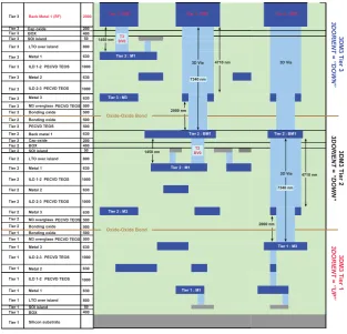
An overview of the MIT Lincoln Labs (MIT LL) manufacturing process is given
below. It is a three tier, 150 nm wafer scale 3D integration process. It features a 1.5 V
low-power Fully Depleted Silicon On Insulator (FDSOI) CMOS technology with one layer
of polysilicon, three metal layers per tier and a back-metal layer between the top two tiers,
with an additional metal layer on top of the entire stack.
To maintain some convention, the bottom tier is named A, the middle tier B and
the top tier C. Tier A is closest to the heat sink, where as all inputs and outputs to the
chip connect to tier C. The figure 2.1 gives an idea of the vertical organization of the stack.
This picture is courtesy of MIT Lincoln Labs Process Guide.
The MIT LL process fabricates 3 tiers separately and then combines them into a
MITLL Low-Power FDSOI CMOS Process: Design Guide
MISCELLANEOUS
92 Rev.: 2008:5 (Sep. 08) Comprehensive MITLL FDSOI design guide Figure 7-7: Thickness stack for three-tier structure with actual layer thicknesses indicated. Final overglass is not shown.
Back metal 1
Back Metal 1 (RF)
630 Tier 3
Tier 3
Cap oxide 200
Tier 3 BOX 400
Tier 3 SOI island 50
Tier 3 LTO over island 800
Tier 3 Metal 1
630 Tier 3 ILD 1-2 PECVD TEOS
Tier 3 Metal 2
630 Tier 3 ILD 2-3 PECVD TEOS
1000
Tier 3 Metal 3
630 Tier 3 M3 overglass PECVD TEOS Tier 3 Bonding oxide
2000
Tier 2
Tier 2 Bonding oxide
Tier 2 PECVD TEOS
Tier 2 Cap oxide 200
Tier 2 BOX 400
Tier 2 SOI island 50
Tier 2 LTO over island 800
Tier 2 Metal 1 630
Tier 2 ILD 1-2 PECVD TEOS 1000
Tier 2 Metal 2 630
Tier 2 ILD 2-3 PECVD TEOS
Tier 2 Metal 3 630
Tier 2 M3 overglass PECVD TEOS 1000
Tier 2 Bonding oxide
500 Tier 1 Bonding oxide
500 500
500
Tier 1 M3 overglass PECVD TEOS 1000
Tier 1 Metal 3 630
Tier 1 ILD 2-3 PECVD TEOS 1000
Tier 1 Metal 2 630
Tier 1 ILD 1-2 PECVD TEOS 1000
Tier 1 Metal 1 630
Tier 1 LTO over island 800
Tier 1 SOI island 50
Tier 1 BOX 400
Tier 1 Silicon substrate
Tier 3 : BM1 Tier 3 : BM1 Tier 3 : BM1
Tier 3 : M1
Tier 3 : M3
Tier 2 : BM1 Tier 2 : BM1
Tier 2 : M3
Tier 2 : M1
Tier 1 : M3
Tier 1 : M1
500 500 500 500 1450 nm 1450 nm 4710 nm 3D Via 2000 nm 7340 nm T2 BV0 T3 BV0 7340 nm
3D Via 4710 nm 3D Via
2000 nm
Oxide-Oxide Bond
Oxide-Oxide Bond
3DM3 Tier 3
3DORIENT = “DOWN”
3DM3 Tier 2
3DORIENT = “DOWN”
3DM3 Tier 1
3DORIENT = “UP”
REVIEW COPY
The capabilities of the MIT LL process can influence the selection of the memory.
The absence of the ability to realize large capacitances can obviate the choice of the DRAM.
The choice of memory is explained in detail in the following section.
2.2
Selection of Memory Type
A memory element is required in order to store the input data on which the
FFT computation is to be performed. Thorolfsson in [6], shows the variation of memory
bandwidth against resolution for SAR processor in the figure 2.2.
0 GB/sec
30 GB/sec
60 GB/sec
90 GB/sec
120 GB/sec
150 GB/sec
1cm
2 cm
4 cm
8 cm
15cm
30 cm
Figure 2.2: Memory Bandwidth v/s Resolution
The factors involved in selection of memory are:
1. Size of Memory - The resolution impacts the size, and hence the selection, of the memory. The SRAM requires four transistors for storage. Also, for each additional
port an SRAM needs two additional transistors.
A Dynamic Random Access Memory (DRAM) requires one transistor and one
one additional transistor. Hence, the DRAM is denser (4x) than the SRAM for the
same no. of bits.
2. Realizable Capacitance - The last values of capacitance required by DRAM, are realized in DRAM Trench technology. However, that process is not available on the
current 3DIC run offered by MIT Lincoln Labs. The area impact would be very large
if planar capacitors were realized in existing fabrication technologies. Realizing these
capacitors is also a design risk in a relatively new process.
3. Requirement for Refresh - The DRAM consists relies on dynamic charge stor-age. Owing to leakage in the access transistor, the charge stored on the capacitor is
susceptible to leakage and data corruption is a possibility. To compensate for this,
periodic refresh is required. Refresh entails periodically reading data out and writing
data back to the same location. This incurs more area for associated circuitry and
more power in the operation.
The SRAM consists of a cross coupled inverter pair which work to maintain each
others’ state. This is an active operation when compared to the DRAM and is not
affected by leakage as much.
4. Speed of Operation - As DRAM circuits rely on sensing the charge stored on a capacitor, the operation is slower compared to an SRAM, where the data is driven
out by an inverter. The presence of a Sense Amplifier is mandatory for DRAMs.
The use of sense amplifiers is optional for SRAM and helps to improve the speed of
the memory. SRAMs are 10x faster than DRAM for this reason.
5. Multiple ports -DRAMs are harder to multi-port as there are multiple avenues for leakage.
SRAMs are driven by active elements and this disadvantage does not arise with each
additional port.
For the aforesaid reasons, we choose an SRAM as the primary data storage element.
This is used to store the input data, the intermediate data (as this is an in-place FFT) and
Table 2.1: DRAM v/s SRAM comparison
Parameter Memory DRAM SRAM
Large Capacitance Required Not required
Refresh Periodical Not required
Speed Slow (1x) Fast (∼5x)
Leakage (Multiple Ports) Affects stored charge Stored charge unaffected
Sense Amplifier Mandatory Not Mandatory
Process Planar Capacitor Not proven Not required
2.3
Components of Memory
The high level diagram of the FFT processor designed by Thorolfsson et al in [3]
is shown in 2.3. The design of the highlighted areas are part of the thesis work and are
discussed in Chapter 3 and Chapter 4.
Figure 2.3: The architecture for 8 Processing Elements in [3]
The section 2.2 concludes that an SRAM is the best choice for the design. There
2.3.1 Storage and Access
The components of this memory would include a Memory Array for storage, Row
Decoders to access data, Precharge circuitry for data read operation and Driver circuitry
for data write operation. The sense amplifier is optional, but is incorporated for making
the design more robust.
2.3.2 Multiplexers
As mentioned in 2.2, the bottleneck for large FFTs is memory bandwidth. One way
to increase the memory bandwidth is to split the processing memory into smaller segments
that can be accessed in parallel. Splitting the processing memory into smaller segments is
the core concept of the architecture of the SAR FFT processor.
The processor splits the processing memory into 32 smaller memories based on
hypercube partitioning scheme thus increasing the memory bandwidth. In this setup in
order to meet all the data dependency requirements of the FFT algorithm each of the
processing elements must be connected to a set of two different memories. In order to allow
this connectivity multiplexers must placed on each of the smaller memories, as shown in
figure 2.3. This presents an overhead not encountered with regular memories, but the area
penalty of the multiplexers is more than compensated for by the increased bandwidth of
Chapter 3
SRAM Design
3.1
Introductory Theory
As mentioned in the previous section, the SRAM is the best choice for the data
memory considering the application and fabrication process. The sections below discuss
the design of individual components of the SRAM, their layout and the integration of
individual blocks to ensure a compact final layout. This layout has to be easily interfaced
with synthesized logic using Through Silicon Vias (TSVs).
The size of each TSV eliminates the possibility to make a single bit cell in 3D. In
this process, the dimensions of a single TSV are 2.5 µm by 2.5 µm and the smallest pitch the vias can be placed on is 3.9µm.
Kaushal explores the design of SRAM for 3DICs in [7] by contrasting divided word
line and divided bit line architectures. His thesis explores both options in 3D, but does not
contrast them with a 2D equivalent. One option is to layout the array on 2D and have
multiple tiers of memory connected using the decoders or bit lines in a 3D fashion. This
approach requires integration of custom memory on synthesized logic and making a memory
in 3D will require a complex integration procedure (making schematics for each tier and
3.2
Cell Design
The basic cell consists of two cross coupled inverters, which retain a state (1,0 or
0,1) across its output nodes. The SRAM requires two lines per bit cell; for the Bit Line
(BL) and its complement, Bit Line Bar (BLB). To access (read) the voltage (or state) of the
cell, only one transistor (either on BL or BLB) is sufficient. To modify (write) a state into
the cell, the cross-coupled inverters have to be overpowered and this requires application of
a differential voltage across the BL and BLB combination.
There are two options to multi-port the design as listed below
1. One big memory - Severely multi port: The disadvantage with this type of arrangement is that for N number of data PEs, there should be N ports available on
the memory array; each basic cell itself has to be N ported. For each additional port,
two transistors are added, complicating the layout of the cell and increasing total
capacitance without increasing the memory storage ability. Tatsumi and Mattausch
in [4] show the inefficiency in resource utilization as the no. of ports in a SRAM/ROM
cell is increased. Plotted areas in 3.1 are normalized to area of the respective 1-port
cell. A severe disproportion is seen in the area used by access transistors v/s storage
transistors.
2. Many small memory - Moderately multi port: An alternate technique is to use an intelligent partitioning scheme and organize the memories as smaller blocks.
Owing to the time multiplexed access of data, not all memory locations are accessed
at the same time and hence each memory needs only one read port and one write port
for efficient operation with minimal area and capacitance.
This decision impacts the design of each bit cell and from the discussion in the
above paragraph, a dual ported cell should be sufficient. The memory and logic partitioning
is done to facilitate such an arrangement. In the dual ported design, one port is dedicated
to the read operation and one port is dedicated to the write operation.
This requires a total of 8 transistors (4 for the cross coupled inverters and 2 each
for the two ports). The cell is designed as per Cell Ratio (CR) and Pull Up Ratio (PR)
guidelines with the PMOS being the weakest, the NMOS access transistors being stronger
and the the NMOS pull down transistors being the strongest.
Exceptions to the above rule have shown to give a smaller area without impacting
the design margins severely. However, in the interest of keeping the design robust, a straight
forward 2:1 length ratio is maintained between pull up transistors to access transistors.
Similarly, a 1:2 width ratio between access transistors to pull down transistors is adequate.
It is important to keep the layout of the cell as compact and symmetrical as
possi-ble. This ensures that neighboring cells tie neatly with each other and with the peripheral
circuit. A good understanding of the array layout is essential even before laying out the
basic cell. Usually, the word lines are drawn horizontally across the cell, while the bit lines
are drawn vertically. The power and ground rails are drawn horizontally, resulting in
neigh-boring cells sharing one rail. Each row of cells share either the VDD rail or ground rail with
the cell above/below it.
Figure 3.3: Layout - Bit Cell
The layout drawn is made as compact as possible and the area of one bit cell in
3.3
Decoder Design
The decoder can be dynamic or static. A dynamic decoder requires to be clocked
and this can create difficulties in a 3DIC environment and clock distribution challenges
are documented by Mineo in [8]. In order to avoid skew issues impacting the word access,
it is decided to use a static decoder. The smallest block of memory element is 32 words
long (with each word having 64 bits in it) and this requires a 5:32 decoder. The decoder
should be strong enough to drive access transistors for 64 cells relatively quickly (total 128
transistors at 2 access transistors per cell).
Literature survey indicates that arrays can be as wide as 128 bits without the
necessity for column decoding. Since the array width is 64 bits, column decoder is not used.
The design of the 5:32 decoder requires hierarchy because of the following reasons:
• Increase in no. of transistors - If a non-hierarchical decoder is built, a total of 11 transistors per row (including the transistor for enable signal) are required. For a
5:32 decoder, the number of transistors are
T RAN SIST ORStotal =T RAN SIST ORSper row×ROW S = 11×32
= 352
When the same design is implemented hierarchically as a 2:4 connecting to four 3:8
decoders, the total number of transistors is
T RAN SIST ORS5:32=T RAN SIST ORS2:4+DECODERS3:8×T RAN SIST ORS3:8
= 5×4 + 4×(7×8)
= 20 + 4×56
= 20 + 224
= 244
The hierarchical decoder requires fewer transistors compared to the non-hierarchical
version and hence is a good choice. The table 3.1 summarizes the no. of transistors
Table 3.1: Types of decoders and no. of transistors
Option No. of transistors
No hierarchy 352
1:2 → 4:16 272
2:4 → 3:8 244
• Logical effort - Sutherland explains logical effort in [9]. While driving a set of capacitances it is advisable to opt for a hierarchical structure as it gives better drive
strength for the same transistors sizes because of the structure.
• Layout congestion -It is tougher to accommodate 11 transistors (for a non-hierarchical structure) in a row and make it pitch match to the SRAM cell. It is easier to
accom-modate 6 transistors (for the 3:8 decoder) in this situation.
Considering all the above points, it is best to organize the structure hierarchically
as a 2:4 decoder followed by a 3:8 decoder. The two-input NOR structure shown in 3.4 is
used in the 2:4 Decoder shown in figure 3.5.
Figure 3.4: Schematic - 2 input NOR gate
The three-input NOR shown in figure 3.6 is used in the 3:8 Decoder shown in
Figure 3.5: Schematic - 2:4 Decoder
Figure 3.7: Schematic - 3:8 Decoder
Each output of the 2:4 decoder is connected to the enable of the 3:8 decoder,
re-sulting in a 5:32 decoder. The lines connected to the 2:4 decoder are the most significant
bits A4, A3 and the lines connected to 3:8 decoder are A2, A1, A0.
Figure 3.8: Schematic - Decoder Integration
The layout of the 2:4 decoder and 3:8 decoder is shown in figure 3.9 and 3.10
Figure 3.9: Layout - 2:4 Decoder
The 2:4 decoder shown in 3.9 utilizes an area of 27 µm×25 µm (675 µm2). The 3:8 decoder shown in 3.10 utilizes an area of 22 µm × 42 µm (924 µm2). When used hierarchically, the 5:32 decoder utilizes an area of 35µm ×176 µm (6160µm2). The row decoder is as long as the array, as it has to be pitch matched and drive each row.
In order to drive the large capacitance on word lines, buffers are added between
output of the row decoder and the array word lines. Stage 1 has 4×PMOS width and 2×
NMOS width with Stage 2 having 4× PMOS width and 8× NMOS width is required to
drive the load to favor the quick discharge of the deactivated word line.
Another identical decoder is used for the write port. The read decoder is connected
to the read access transistors of the cell and the write decoder is connected to the write
access transistors of the cell. The decoders are identical in design and layout.
The controller which selects the words out of the memory should read out the
contents of one memory locations then, after a time duration equal to the latency through
the processing logic, it should write the data back to the same memory location. This
means that the addresses given to read port should be given to the write port after a delay
3.4
Sense Amplifier Design
A sense amplifier is designed to lend robustness to the circuit operation. The
sense amplifier is enabled on each cycle that a read is required, so that the bit cells can
drive a voltage onto the bit lines and the result is reflected on the output of the sense
amplifiers. The sense amplifier is reset at the end of that cycle and is enabled when CLK
is low and Read Enable signal is high. Kelkar [10] contrasts between voltage sensing and
current sensing for an SRAM design. The current sensing circuit is more power hungry and
hence the circuit in 3.11 is used.
The transistors M1 and M3 are used to precharge the internal nodes of the sense
amplifier. The internal nodes are precharged to VDD when ENABLE is low and the status
on BL and BLB is evaluated when ENABLE is high. The cross-coupled inverter pair formed
by M2, M0, M5 and M4 is designed to store the value on BL and BLB until it is reset by
turning ENABLE off. Transistor M8 provides a path to ground for either M7 or M6.
Figure 3.11: Schematic - Sense Amplifier
When reading a cell with a logic 1, the BL line is driven to logic high and the BLB
line is driven to logic low. This voltage on the bitlines turns on M7 and turns off M6. This
the gates of the inverter formed by M0 and M4, pulling the SA net high.
When reading a cell with a logic 0, the BL line is driven to logic low and the BLB
line is driven to logic high. This voltage on the bitlines turns off M7 and turns on M6. This
pulls down the source of M4 and hence the drain of M4. The drain of M4 is the SA net and
is pulled low and retained as this level due to the action of the two inverters.
Figure 3.12: Layout - Sense Amplifier
3.5
Write Driver Design
The Write Driver is one of the critical parts of the SRAM design. The data that
is given to the memory array should be differential, but the data received from the logic
processing element is single-ended. The write driver has to convert the data to differential
and be strong enough to drive the bit-lines to the given state (1,0 or 0,1). Just as the sense
amplifier is connected to the read bit lines, the write driver is connected to the write bit
lines.
Figure 3.13: Schematic - Write Driver
When DIN signal is logic 1, M0 is on and M1 is turned off through inverter realized
by M2 and M3. This results in the BLB net being pulled down and a logic 1 being written
into the cell. When DIN signal is logic 0, M0 is off and M1 is turned on through the inverter
combination. This pulls down the BL net and a logic 0 is written into the cell. The layout
Figure 3.14: Layout - Write Driver
3.6
Precharge Circuit Design
The Precharge circuit is required for an SRAM such that the bit lines are pulled
to a known value each cycle and are equalized. Typically this happens in the positive half
of the clock cycle and is realized using 3 PMOS transistors (M3, M4 and M5) connected as
shown. The speed of operation of the memory is not the bottleneck and hence the precharge
transistors are minimum sized. The precharge works during the positive half of the clock
cycle for a read operation (ENABLE is high). The NAND combination (M0, M6, M1 and
M2) ensures that a logic 0 is driven only when both CLK and ENABLE are high, turning
Figure 3.15: Schematic - Precharge
3.7
Integrating Multiplexer into Array
As mentioned in section 2.3.2, there are a total of 32 memory blocks and each of
the memory blocks should have the capability to interface with two logic elements.
The two IO ports are termed as A and B. For the read port, data from the output
of the sense amplifier is to be given to either port A or port B and the controller decides
this. This is a demultiplexer operation.
For the write port, data from either port A or port B are given to the write drivers
of the array. This is realized using a straight forward circuit. The passage of the correct
voltage level to/from the memory array has to be ensured. This is the multiplexer operation.
The multiplexer/demultiplexer should pass a voltage of 0V and VDD without a
drop and this requires a complementary pass transistor logic (PMOS to successfully pass
VDD and NMOS to successfully pass 0V). A transmission gate structure is employed to
ensure that the voltage levels are faithfully passed through.
Figure 3.17: Schematic - Multiplexer
The multiplexer circuit is the interfacing block between the logic and memory.
Since each memory block on the middle tier is connected to the logic elements on the tier
above and the tier below, two types of multiplexer instances are required. The first one
has a Through Silicon Via (TSV) going from tier B (middle) to tier A (bottom) and the
second one has a TSV from tier B (middle) to tier C (top). These multiplexer blocks are
placed near the write drivers and the demultiplexers are placed near the sense amplifiers.
Figure 3.18: Layout - Multiplexer
3.8
Layout
The layout of the entire array is crucial to the success of the project. The layout
should be compact and have all the I/O ports available on the periphery of the array to
accommodate the large inter-tier through silicon vias (TSVs).
The memory array has been placed in the center of each layout with the read port
row decoders on the left and write port row decoders on the right.
The write drivers are placed to the North of the memory array and the sense
amplifiers are placed on the South of the memory array. This is done as the TSVs are
located only at the north and south of the memory array. The TSVs corresponding to the
reading data (i.e. transferring data from the output of the memory to input of logic) are
located at the south side after the sense amplifiers. The TSVs corresponding to the writing
data (i.e. transferring data from the output of the logic to input of memory) are located at
the north side before the write drivers.
The A IN or B IN enables the correct mux and directs data from either A[63:0] IN
or B[63:0] IN to the write drivers. The write driver circuit asserts bitlines in accordance
with the data. When WRITE EN is high, WA[4:0] dictates the row asserted by the write
row decoder.
The CLK and READ EN signals enable the precharge circuit when both are high.
When READ EN is high, RA[4:0] dictates the row asserted by the read row decoder.The
Sense Amplifier is enabled when CLK is low and READ EN is high. The A OUT or B OUT
Figure 3.19: Conceptual Layout
3.9
Comparison of Custom Memory against CACTI
The layout of 32×64 bits cells occupy 600µm x 180µm (area of 0.108 mm2) out of a total array area of 691µm x 225 µm (0.155 mm2). The area per bit is 75.68 µm2. For the given memory size and technology node, CACTI 4.1 [11] gives the area of memory as
0.085 mm2. The designed memory has 3D specific components like multiplexers and TSVs,
hence the comparison is valid.
The CACTI memory operates with an access time of 0.85ns, while the custom
de-signed memory operates at 1.7ns. This operating frequency of 588 MHz is not the bottleneck
for the system as the logic operates at 78 MHz.
For the custom memory, energy for a write operation is computed as 5.8 pJ and
energy for a read operation is computed as 26.16 pJ. When this is amortized over the
number of bits, the energy per write / bit is 90.78 fJ/bit and energy per read / bit is 408.78
fJ/bit. For the system, the number of reads and writes are equal and hence the average
access energy per bit can be taken as 250 fJ/bit. However, the dynamic read energy from
CACTI is 166 fJ/bit and the dynamic write energy is 59.21 fJ/bit.
3.10
TSV Placement
Through Silicon vias are inter-tier vias that enable the integration of the tiers.
Since these tiers have to tie two tiers of silicon (5 µm apart), they need to have a large footprint on the tier they start. This footprint is 1.25 µm x 1.25 µm and is comparable to the layout of a 6T cell. Each such via consumes a lot of area. The location of the vias
is important so as not to interfere with the internal routing, hence they are placed at the
periphery of the array. The number of vias also should be limited to the minimum possible.
In this design, the array needs to contain 64 bits with each array requiring multi-ported
capability (one for read and one for write). Also, as per the high level design, each array
should contain a multiplexer in built, resulting in doubling the number of input/output
pins. Hence, the total number of input/output pins is 256 per array of 32 x 64.
Total number of TSVs = 32×256
The decision to place the memory block on a particular tier was taken later in the project.
The location of the tier, impacts the type of vias that are to be placed around the array.
3.11
Integrating Array with Standard Cell Layout
In a standard cell ASIC design, the power and ground rails are striped across the
chip at regular distances. The cells are designed such that they pitch match these lines, i.e.
have a horizontal VDD stripe on one end and a horizontal GND stripe on the other end.
Each memory array is a standalone block that is designed independently of the
power and ground stripes in the standard cell ASIC, but still it requires power and ground
connections to it.
For each cell, a write and read operation is performed. The cell is symmetric and
the current to store a 0 is same as current required to store a 1. The total power dissipation
in this operation is 0.7455 µW. Since, the supply voltage is 1.5V, the current drawn is calculated as
0.7455µW
1.5V = 0.49µA (3.1)
Since there are 64 cells in a row, the total current drawn by one row is
= 0.49µA×64 = 31.8µA (3.2)
The MIT LL design guide [2] talks about says that the minimum current density
to avoid electro migration is 3mA / µm2. The peak currents in the system for a series of
read and writes is 24mA, but this is for a relatively short duration of time. For a series of
4 read/write operations carried out over 10ns, the power dissipation is 6.16 mW.
The average current drawn from the supply (VDD) of 1.5V is
Iavg =
Ptot
VDD
= 6.16mW
1.5V = 4.1mA (3.3)
Going by the guidelines of 1.5mA / µm, the power delivery rails to the system should be sized to accommodate this current
Width = 4.1mA
1.5mA/µm = 2.73µm (3.4)
This is the total width of metal, that should tie the power and gnd rails to the
As each memory is to be finally integrated with a standard cell design, the number
of power and ground lines are limited. Each power/gnd rail is 0.8 µm wide and the pitch of GND rails is 24 µm. The total height of the memory array designed is 225 µm.
Total rails = 225µm 24µm
= 10
As each rail is 0.8 µm wide, the total width of 8 µm (on VDD and GND each) should be sufficient to provide the required current consumption.
The design guide indicates that current density of less than 1mA per via should
provide reasonable short-term reliability. We might need about 6 vias each time the VDD
and GND change layers. Since the power and ground are present in metal 1, we do not
need the vias mentioned above.
3.12
Checking Basic Working of Memory
The logic elements should interact with the Row Decoders, Write Drivers and
Sense Amplifiers on the memory side. It has to be ensured that there exists a voltage
level compatibility between the logic and memory. Since system level simulations are time
consuming and not practical for a system this large, the VOH, VIH, VOL and VIL levels
are entered into the invec (input vector) and outvec (output vector) files during HSPICE
simulations of the memory array. The levels are set as indicated below:
1. VOH = 1.2 V
2. VOL = 0.1 V
3. VIH = 1.0 V
4. VIL = 0.2 V
To ensure the proper working of the memory, the following experiments are
30
1. Experiment: The read Static Noise Margin (SNM) and Write Noise Margin (WNM) are calculated using the procedure mentioned in [12].
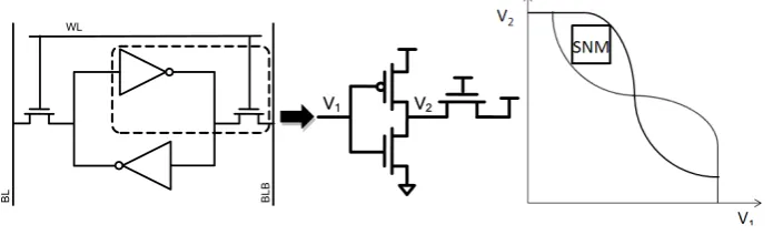
The figure below shows how to compute the read static noise margin (SNM) of the
cell. First, the feedback from the cross coupled inverters is broken. Next, the Voltage
Transfer Curve (VTC) of the inverter formed by half of the SRAM cell is found by
sweeping V1 (inverter’s input) from 0 to VDD and measuring V2 (inverter’s output).
This plot is then used to construct the butterfly plot that is representative of the two
halves of the cell driving each other. The read SNM is the side length of the maximum
possible square that can fit inside of the butterfly plot.
by teams of two students. The first two phases of the project will consist of well-defined tasks (similar to the homeworks), while the final (longest) phase of the project will be much more open-ended.
PHASE 1: Cell Characterization and Decoder Design (due Thursday, Nov 1, at 5pm)
Cell Characterization:
In the first phase of the project, you are provided with a pre-designed SRAM cell. Characterize the cell stability by using Cadence to obtain an extracted netlist and HSPICE to perform simulations to get the read and write margins.
To obtain the SRAM cell:
- In Cadence, create a library “sram” linked to the TSMC 0.24um technology (see lab
2).
- Create a layout cellview “sram_cell”. Do not close the cellview.
- Create a schematic cellview “sram_cell”. Do not close the cellview.
- Create a symbol cellview “sram_cell”. Do not close the cellview.
- Now in an x-terminal, go to the directory ~/ee141/sram/sram_cell/ and type the
following commands:
cp ~ee141/project/sram_cell/schematic/* schematic cp ~ee141/project/sram_cell/layout/* layout cp ~ee141/project/sram_cell/symbol/* symbol Reply “y” to all “overwrite” prompts.
- Go back to Cadence and close all open cellviews. Now reopen the symbol, schematic
and layout views of sram_cell. You should see the SRAM cell design.
Figure 2. SRAM Read Static Noise Margin.
Recalling that the wordline and bitlines are held at VDD during a read, Figure 2 shows
how to extract the read static noise margin (SNM) of the cell. First, the feedback from the cross coupled inverters is broken. Next, the VTC of the “inverter” formed by half of the
SRAM cell is found by sweeping V1 (the inverter’s input) from 0 to VDD and measuring
V1 V2
WL
BL BLB
Figure 3.21: Read - Static Noise Margin Experiment
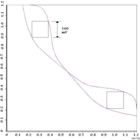
The maximum voltage at V2 when V1 is at 1.1V is 0.16V. The SNM is shown below.
The side of the maximum square that can fit is about 160 mV.
To compute write SNM, VDDis applied to the wordline (to switch on the pass
transis-tor) and the value to be written into the memory cell is driven onto the bitlines. The
figure below shows how to extract the write noise margin (WNM) of the cell. Again,
feedback from the cross coupled inverters is broken, and the VTC of the inverters
are measured. Note that in this case the VTCs of the two halves of the SRAM are
no longer the same (since one of the bitlines is driven to 0V and the other to VDD).
These VTCs are used to create the plot in figure 3.23. The write SNM is 0.5V.
2. Experiment: The SRAM schematic with parasitics extracted from the model files. The simulation is performed over a 10ns time with a clock of 2ns (500 MHz). The
vector files are set up to show the operations in table 3.2.
Figure 3.22: Read - Static Noise Margin Plot
V2 (the inverter’s output). This plot is then used to construct the “butterfly plot” that is
representative of the two halves of the cell driving each other. The read SNM is the side length of the maximum possible square that can fit inside of the butterfly plot. You do not have to calculate the size of this maximum square, but you should submit the butterfly plot (generated using HSPICE) that graphically indicates the SNM. You should also measure the worst-case voltage rise in the SRAM cell during a read (i.e., the value of V2
when V1 is at VDD) and provide that value in your report.
Figure 3. Write Noise Margin.
During a write, VDD is applied to the worldine, and the value to be written into the memory cell is driven onto the bitlines. Thus, Figure 3 shows how to extract the write noise margin (WNM) of the cell. Again, the feedback from the cross coupled inverters is broken, and the VTC of the “inverters” are measured. Note however that in this case, the VTCs of the two halves of the SRAM are no longer the same (since one of the bitlines is driven to 0V, and the other to VDD). These VTCs are used to create a butterfly plot, and
the WNM is the side length of the largest square that can fit inside of the butterfly plot. You do not have to calculate the WNM, but you should generate the butterfly plot (again using HSPICE) and graphically indicate the WNM. You should however measure the worst-case cell voltage during a write (which is found from measuring V1 when V2 is at
0V).
Layout of SRAM Array:
Figure 4. Arraying Procedure V2
V1 V1 V2
Figure 3.24: Write Noise Margin Plot
Table 3.2: Read Write sequencing for SRAM
Steps Read Port Read Address Write Port Write Address
Step1 NA NA A 12h
Step2 A 12h B 09h
Step3 B 09h B 15h
Step4 A 15h A 07h
Step5 B 07h NA NA
the results are tabulated in 3.3.
Table 3.3: SRAM temperature operation
Temperature (0C) Power Dissipation (mW)
-40 6.697
25 8.784
90 7.927
4. Experiment: While comparing the schematics and layout simulation the differences in power dissipation were observed and table 3.4 was created. This difference is due
to the coupling capacitances that are included while performing parasitic extraction
of layout. Both designs are run at 500 MHz with a pattern of 4 read and 4 write
Table 3.4: Comparison for SRAM: Schematic v/s Layout
Parameter Schematic Layout
Charge (Q) pC 51.3 60.80
Energy (E) pJ 61.6 72.9
Power (P) mW 6.16 7.29
This information is useful in understanding the effect of coupling capacitances and help
to estimate the increase in power dissipation by using the schematic power dissipation
numbers, before actually creating an elaborate layout.
5. Experiment: To determine the access time of the SRAM, a value is first written to a given location and on the next cycle a read from that location is performed. The
waveforms in figure 3.25 show the following information:
(a) Time taken for theinternal bit voltages to flip on the positive half cycle of CLK cycle 2
(b) Time taken for thebitlines to prechargeon thepositive half cycle of CLK cycle 3
(c) Time taken for theoutput to be drivenon thenegative half cycle of CLK cycle 3
The SRAM can operate correctly with a clock period of 1.7ns giving a clock frequency
of 588MHz. The average power dissipation over one write and one read cycle is 12.28
Chapter 4
ROM Design
4.1
Introductory Theory
Twiddle factors are required for the computation of the FFT. These twiddle factors
do not change in the course of computation of the FFT and are stored in a ROM. The benefit
of having a ROM is that it takes lesser area (than an SRAM) for storing same number of
bits. Also, a ROM is non-volatile and eliminates the need for loading the twiddle factors
on power up. This simplifies the system design.
A ROM needs a precharge circuit (for getting the output to a known state each
cycle) and this is realized by pull-up PMOS transistors. The no. of bits required in each
ROM structure is organized as 129 x 54. The decoder layout is a crucial part of the design
as the pitch matching is not easily realized due to the large size of decoder and small size
of the cell (only one pull down transistor).
4.2
Memory Element
In the ROM structure, there is a pull up structure common to all bitlines and a
transistor is present at each location (intersection of bitline and address line) where a logic
0 is to be read. The absence of a transistor means the line is automatically pulled up (using
the precharge) and this indicates a logic 1. The structure that stores the data for a logic 1
Figure 4.1: ROM - Schematic Logic 0 and Logic 1
4.3
Decoder Design
The decoder designed here is again a static decoder, but has 8 inputs and 129
output lines. As 7 inputs can control 128 outputs, the MSB is directly given to one row
without passing through the decoder structure. This simplifies the task to two decoder
structures, a 7:128 and a 1:1 decoder. The 7:128 decoder structure is disabled when the
MSB is high.
The decoder is constructed using the same concerns shown during the design of
the decoder for the SRAM. However, the cell has only one transistor in it and typically even
a hierarchical 7:128 decoder structure has about 15 transistors per row address. Owing to
the mismatch in width between a row of the decoder and a row of the array, it is difficult to
align the decoders to the array (pitch match). Hence an innovative strategy is implemented.
The odd addresses are decoded on the left side of the array and even addresses on the right
side. This requires the decoder to be split and alternate addresses interleaved within the
array. This results in a more compact layout.
The 7:128 decoder design is now simplified given that A0 is used as the control
bit between ODD and EVEN 6:64 row decoders. The 3 most significant bits after A7 (i.e.
A6, A5, A4) are given to a 3:8 decoder (DECODER A) and the each of the 8 output of the
DECODER A are used as a enable signal for eight other 3:8 decoders, which finally drive
the word lines.
The row decoder is constructed on both sides of the array with the odd addresses
being decoded on the left side of the array and the even addresses being decoded on the
and ODD row decoder on the left side is disabled. When A0 is low the ODD row decoder
is enabled and EVEN row decoder is disabled. High Level diagram shown in figure 4.2.
Figure 4.2: ROM Address Decoding
4.4
Layout
The pull up transistors (precharge) circuit are placed on one side (NORTH) of the
array and the output is taken from the SOUTH side of the array. This ensures that the
output read is correct as the change has to propagate through the entire length of the array.
The layout is generated automatically by reading a file which has the contents of
the ROM. SKILL code is written such that transistors are placed at locations where a 0 is
read from the file, and no transistor is placed at a location where 1 is read from the file.
This avoids the manual work of placing transistors on a grid and also helps to change the
layout easily if the contents of ROM are altered later. Thus, a compact layout is realized,
by placing transistors at minimum DRC clearance from each other. The row decoders and
precharge circuitry is put in later and tied together to form the complete layout of the
Figure 4.3: ROM - Layout
The ROM layout in figure 4.3 shows the odd and even decoders, the precharge
and sections of the layout where transistors are placed. The total area for ROM having 54
×129 bits of memory is 93µm×354µm (0.032922 mm2), giving an area of 4.72 µm2 per bit.
4.5
Experimental Results
The logic elements need to interact with the row decoders (by giving the address
required) and read the output data from the output bit lines of the ROM structure. It has
to be ensured that there exists a voltage level compatibility between the logic and memory.
Since system level simulations are time consuming and not practical for a system this large,
the VOH, VIH, VOL and VIL levels are entered into the invec (input vector) and outvec
(output vector) files during HSPICE simulations of the memory array. The levels are set as
indicated below:
1. VOH = 1.2 V
2. VOL = 0.1 V
3. VIH = 1.0 V
1. Experiment: The design of the ROM is automated based on a text file as input. It is important to check that the transistors are placed in the correct location and the
voltage levels at the output, as required by the logic, are being met by the designed
circuit. The ROM is asynchronous and during the simulation the data from row 0
to row 129 is read out every 2ns. The power dissipation observed in this case is 5.44
mW. A comparison of schematic versus layout is shown below.
Table 4.1: Comparison for ROM: Schematic v/s Layout
Parameters Schematic Layout
Charge (Q) nC 1.1844 1.3796
Energy (E) pJ 1.421 1.6555
Power (P) mW 5.44 6.36
2. Experiment: To determine the access time of the ROM, all locations are read. The input address is changed every 1ns. The effect of precharge is visible in bursts, when
there is a change in input address causing the precharge to momentarily dominate.
The precharge results in longer pulses when no transistor is present at the memory
location addressed by the row decoder.
Figure 4.4: Read operation - ROM
The ROM can operate correctly with a clock period of 1ns giving a clock frequency of
1GHz. This frequency far exceeds the operating frequency of the logic. The average
power dissipation over 129 cycles of reading from the ROM is 8.88 mW and energy
Chapter 5
Thermal Analysis
5.1
Introductory Theory
One of the major drawbacks while considering 3DIC for any application is the
thermal impact on the circuits. In conventional 2DICs, the heatsink can be connected
to the die with minimal thermal resistance resulting in quick heat transfer from the heat
generation source to the sink. For 3DICs, as wafers are stacked and there is moderate
thermal conductivity for heat generated in internal layers to reach a dissipation source
(such as a heatsink), thermal analysis plays an important part. In this section, we calculate
the power dissipation of the designed circuit while varying certain parameters. The power
dissipation is a direct indication of thermal impact.
One of the important parameters while designing is the scalability of the circuit.
In the coming sections, an effort is made to capture the power dissipation for the smallest
independent circuits for the most frequent operations, hence giving an idea of the variation
in power dissipation while increasing the array (in both L and W). [13]
5.2
Cell Read
This section aims to capture the power dissipation associated with a cell read.
Only the power dissipation from the cell is captured by connecting the cell transistors to a
separate VDD and measuring the current drawn from that supply. The other circuits which
source for the purposes of this experiment.
Since the cell is symmetrical there should not be a difference when reading out a
(1,0) or (0,1) from the output of the internal cross-coupled inverter. Also, since there is
only one read port, we use that to access the data stored internally.
5.3
Cell Write
For the Cell Write, two situations can occur as illustrated below.
• Same Value written - This situation occurs when the value inside the cell is the same
as that is being written into it.
• Different Value written - This situation occurs when the value inside the cell is different
from that which is being written into the cell. This results in a higher power dissipation
that the operation mentioned above.
The power dissipation corresponding to each cycle is calculated while performing
a single experiment with the sequence of events shown in 5.1
Table 5.1: Power Dissipation per operation
Operation Power Dissipation (µW) Comment
Dummy operation 1.19 Write a logic 0
Different value write 0.801 Write a logic 1
Same value write 0.0176 Write a logic 1
Read 0.1134 Read contents
5.4
Decoder Word Line Select
The decoder is used to turn on one row of transistors, so that the data stored
internally can be captured on the bitlines. For each additional bit, two transistors are
added to the word line. As the capacitance increases, the power dissipation in the decoder
also increases linearly. Figure 5.1 shows the increase in power dissipation and rise/fall times
Figure 5.1: Rise/Fall times and Power dissipation v/s capacitance - Decoder
5.5
Write Driver
As the number of rows increases, the capacitance on the bitlines increases and this
results in a greater amount of charge being stored on the bitlines. However, since only the
read bit lines (RBL, RBLB) are being precharged and are separate from the write bit lines
(WBL, WBLB), the only charge that is to be discharged is that stored internal to the cell.
The capacitance of longer bit lines will not impact the power dissipation in the write driver
circuit.
5.6
Sense Amplifiers
The sense amplifier is not driving the bitlines and the power dissipation is not
impacted by variation in the number of rows in the array. However, the sense amplifier is
supposed to drive the flip flops at the input of the logic path.
5.7
Precharge
Precharge circuit can be thought to be the opposite of the write driver circuit. The
write driver strives to create a differential voltage such that one value (1,0 or 0,1) is written
into the cell. The precharge circuit strives to equalize the voltage on the bitlines so that
the cell can drive its internal value out onto the lines. As the number of rows increases, the
transistor S/D contacts on the precharge transistors increase. Figure 5.2 shows the increase
Figure 5.2: Rise/Fall times and Power dissipation v/s capacitance - Precharge
5.8
Percentage Power dissipation
Each block of the circuit dissipates a certain amount of power and it is important
to characterize the percentage, if not the absolute values, of power dissipation in each of
the blocks. This is done by assigning a separate power supply connected to each block
and it’s sub-blocks. The current through these power supplies is measured and the power
dissipation is computed.
A split up of power dissipation for a write followed by a read for various blocks is
given in the table 5.2.
Table 5.2: Circuit Blockwise power dissipation - write and read
Name of Block Power Dissipation (µW) Percentage of Total (%)
Read Row Decoder 690 15.44
Write Row Decoder 688 15.39
Sense Amplifier 5.37 0.12
Precharge 2680 59.96
Memory Array 396 8.86
Write Driver 4.2 0.09
Multiplexer 6.44 0.14
Total 4470 100
Figure 5.3: Pie Chart: Power dissipation in various blocks - write and read
Similarly, a split up of power dissipation only for a write is given in the table 5.3.
Table 5.3: Circuit Blockwise power dissipation - write
Name of Block Power Dissipation (µW) Percentage of Total (%)
Read Row Decoder 875 64.44
Write Row Decoder 478 35.17
Precharge 2.73 0.2
Memory Array 2.52 0.185
Total 1360 100
A plot of percentage power for write operation is shown in figure 5.4.
For each additional cell added to a row, the Gate-Source capacitance of two
tran-sistors (RA1, RA2 for read decoders and WA1, WA2 for write decoders) plus wiring
capac-itance are added.
The power dissipation is directly proportional to the capacitance. For the
sce-nario, the bulk of the capacitance is due to the Gate-Source connections and some part is
contributed by wire capacitance. An approximation can be made that the power dissipation
in a decoder varies linearly as the Gate-Source capacitance connected to it. Hence, if the
width of the array is made 32 bits, instead of 64 bits, the power dissipation would drop by
half. Likewise, if the number of rows are reduced, the power dissipation would drop by half.
5.9
Operating Temperature Range
The memory element designed in this project is encapsulated by two tiers of logic.
The combined 3D unit will be packaged and ultimately used in imaging application for
an unmanned aerial vehicle. This means that the design should meet military standard
specifications. The maximum external temperature is 125 0C and a temperature of about
175 0C can be assumed as the internal ambient that the memory is supposed to operate
under.
A temperature sweep is conducted from 10 0C to 200 0C and the the memory
operations are checked for errors, by writing to a memory location and then reading from
Chapter 6
Conclusion
6.1
Summary
In summary, a SRAM of 32 rows x 64 bits wide was designed to support the
FFT Processor and demonstrate memory on logic in 3D IC technology. Multiplexers to
write to the SRAM and Demultiplexers to read from the SRAM were also designed and
integrated with the memory block. TSVs are placed on the data input and output lines,
on the periphery of the array, to ensure easy integration with Processing Elements on other
tiers. Power and Ground rails are passed through the array, so as to enable continuity of
supply rails throughout that layer.
The area for the SRAM is 0.155 mm2 (75.68µm2 per bit). The access time for the SRAM is 1.7ns. The energy for read access is 408.79 fJ/bit and write access is 90.78 fJ/bit.
A ROM was designed to ensure compact storage of twiddle factors. The ROM
was tested and integrated with the Processing Elements. The ROM is placed on the outer
two tiers and the address inputs are from the controller. The controller is located on the
middle tier and the ROM needs to have TSVs on the address lines in order to connect to
the controller. The output data from the ROM is connected to the Processing Elements on
that tier and does not require TSVs.
Table 6.1: Design Summary
Parameter Static Random Access Memory Read-Only Memory
Size (bits) 32 ×64 54 ×129
Total Area (mm2) 0.155 0.032922
Area per bit (µm2) 75.68 4.72
Access Time (ns) 1.7 1
Read Energy (fJ/bit) 408.79 165
Write Energy (fJ/bit) 90.78 NA
The benefits of memory partitioning and 3D interconnect are quantified in [3]. The
memory and logic are laid out on a single tier and the performance of this 2D system is made
with the 3D system. Partitioning the design into many smaller memories has increased the
area of peripheral blocks per memory (decoders, write and sense circuits), but has resulted
in average wire length reduction (53%), overall area reduction (30.9%) and higher operating
frequency (24.6%) over its 2D counterpart.
6.2
Future Work
The present design is partitioned with SRAM and Controller on the central tier and
the upper and bottom tiers containing the Processing Elements and ROMs. The memory
block designed as part of this work can be used as a building block to create a 3D memory
using one of the architectures (BLsplit, WLsplit) described by Kaushal [7]. The Controller
and Processing Elements should be partitioned to accommodate a 3D Memory. The 3D
Memory can be built using the memory module designed as part of this work.
Leveraging on improvements to the existing process or using a different process,
a DRAM can be designed to work with the existing framework. Area and performance
Bibliography
[1] W. R. Davis, J. Wilson, S. Mick, J. Xu, H. Hua, C. Mineo, A. M. Sule, M. Steer, and
P. D. Franzon. Demystifying 3D ICs: The Pros and Cons of Going Vertical. IEEE
Design And Test of Computers, 22(6):498–510, Nov.-Dec. 2005.
[2] Massachusetts Institute of Technology Lincoln Labs. MITLL Low-Power FDSOI
CMOS Process Design Guide, revision 2008:6 edition, September 2008.
[3] T. Thorolfsson, K. Gonsalves, and P. Franzon. Interconnect and Memory Tradeoffs
in a Distributed FFT Processor Architecture for Synthetic Aperture Radar in 2DIC
and 3DIC. InThe 15th International Symposium on High-Performance Computer
Ar-chitecture, 2009. HPCA’09. Workshop on 3D Integration and Interconnection-Centric
Architectures, 2009.
[4] Y. Tatsumi and HJ Mattausch. Fast quadratic increase of multiport-storage-cell area
with portnumber. Electronics Letters, 35(25):2185–2187, 1999.
[5] Paul D. Franzon, W. Rhett Davis, Michael B. Steer, Steve Lipa, Eun Chu Oh, Thor
Thorolfsson, Samson Melamed, Sonali Luniya, Tad Doxsee, Stephen Berkeley, Ben
Shani, and Kurt Obermiller. Design and cad for 3d integrated circuits. InDAC ’08:
Proceedings of the 45th annual conference on Design automation, pages 668–673, New
York, NY, USA, 2008. ACM.
[6] Thorlindur Thorolfsson. Benefits of Three-Dimensional Integration for Memory Rich
Architectures, Preliminary Examination, North Carolina State University, 2007.
[7] Kaushal Modi. Exploring different architectures for an sram in 3dic technology.
[8] Christopher Mineo. Clock tree insertion and verification for 3d integrated circuits.
Master’s thesis, North Carolina State University, 2005.
[9] I.E. Sutherland, R.F. Sproull, and D. Harris. Logical Effort: Designing Fast CMOS
Circuits. Morgan Kaufmann, 1999.
[10] Indraneel Balakrishna Kelkar. Tradeoffs involved in design of srams. Master’s thesis,
North Carolina State University, 2005.
[11] Download from http://www.hpl.hp.com/research/cacti/cacti4.1.tar.gz.
[12] Project Desc at http://bwrc.eecs.berkeley.edu/classes/icdesign/ee141 f07/Project/EE141
Project1.pdf.
[13] Mesut Meterelliyoz, Jaydeep P. Kulkarni, and Kaushik Roy. Thermal analysis of
8-t sram for nano-scaled 8-technologies. In ISLPED ’08: Proceeding of the thirteenth
international symposium on Low power electronics and design, pages 123–128, New