ISSN(Online): 2320-9801
ISSN (Print): 2320-9798
International Journal of Innovative Research in Computer
and Communication Engineering
(An ISO 3297: 2007 Certified Organization)
Vol. 3, Issue 8, August 2015
DDS Based Phase Locked Loop
Sreelekshmi K R, Subhalekshmi K R, Jacob Thomas
M. Tech Student, Department of ECE, Believers Church Caarmel Engineering College, Kerala, India
M. Tech Student, Department of ECE, Believers Church Caarmel Engineering College, Kerala, India
Assistant Professor, Department of ECE, Believers Church Caarmel Engineering College, Kerala, India
ABSTRACT: The phase locked loop (PLL) has been widely used in wireless communication systems due to the high frequency resolution and the short locking time. A phase-locked loop (PLL) is a closed-loop feedback control system, which synchronizes its output signal in frequency as well as in phase with an input signal. The phase detector, the loop filter, and the voltage controlled oscillator are the key parts of almost all PLLs. The phase-locked loops (PLLs) are probably the most widely used synchronization technique in grid-connected applications. The Direct Digital Synthesis (DDS) is also an emerging and maturing signal generation technology. But another advanced technique in which, DDS signal is mixed with the voltage-control oscillator output in the PLL feedback path. This solution helps in avoiding some of the typical trade-offs in PLL. In particular, it is possible to achieve a very high-frequency resolution together with fast settling and spectral purity. The proposed design consists in describing the mixed behaviour of this DDS-based PLL architecture starting from the specifications of each building block. The HDL models of critical PLL blocks have been described in VHDL-AMS to predict the different specifications of the PLL. The effect of different noise sources has been efficiently introduced to study the system performance. The obtained results are composed with transistor-level simulations to validate the effectiveness of the proposed models. The comparative study showed the performances of different parameters. Finally, DDS- based PLL architecture is better than other architectures.
KEYWORDS: phase-locked loop; direct digital synthesiser; hardware description language; voltage controlled oscillator, digital to analog converter; analog and mixed signal.
I. INTRODUCTION
A phase locked loop is a closed loop control system which is used for the purpose of synchronization of the frequency and phase of a locally generated signal with that of an incoming signal. It is basically a nonlinear feedback loop. The PLL consists of a voltage controlled oscillator (VCO), a phase detector, a variety of dividers, and a loop filter. DDS is an emerging and maturing signal generation technology. DDS consists of phase accumulator, lookup table and DAC converter. In a general PLL synthesizer, the division ratio becomes large if frequency resolution is increased. This decreases the phase comparison frequency. Consequently, the PLL output phase stability is degraded. Because here the reference clock is converted once by the DDS, it is possible to make the PLL phase comparison frequency large enough. It is obvious that spurious components exist in the DDS output, but they can be suppressed by the PLL low pass characteristic. The DDS is installed in the PLL feedback circuit. In this case, too, the PLL phase comparison frequency can be raised by adjusting the DDS output frequency. This also improves the PLL phase stability.
II. RELATED WORK
ISSN(Online): 2320-9801
ISSN (Print): 2320-9798
International Journal of Innovative Research in Computer
and Communication Engineering
(An ISO 3297: 2007 Certified Organization)
Vol. 3, Issue 8, August 2015
against VCO sensitivity [2], Loop filter transfer function for particular application. The main benefit compared that it doesn’t require special high-frequency PLL for DDS clock[4], since it is produced by the VCO of main loop. There is no need in narrow-band high frequency and high cost based VCO [8]. This system show that good accuracy is achieved for both amplitude and frequency parameters.
III. PHASE LOCKED LOOP
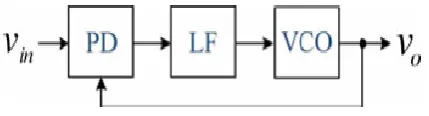
Phase-locked loops (PLLs) are a widely needed and used circuitry in today’s semiconductor chips. They are mainly used for three different tasks: Generation of high frequency on-chip clocks by frequency multiplication, Reduction of clock skew and Jitter attenuation. A PLL is characterized by the frequency range, jitter, jitter attenuation and lock time. PLLs are only used for generation of high frequency stable clocks and are normally feed by quartz controlled oscillators so that there is no need for a jitter attenuation.
Fig. 1. Basic PLL Structure
The phase-locked loops (PLLs) are probably the most widely used synchronization technique in grid-connected applications. The key feature of open-loop synchronization techniques is that they are un- conditionally stable. They typically yield a satisfactory performance in terms of the phase or frequency detection accuracy when the grid frequency is at, or close to, its nominal value; however, their performance tends to worsen when the input frequency deviates from its nominal value. To overcome this problem, incorporating frequency estimation or control algorithms into the open-loop schemes have been proposed.
The main challenge that is associated with the PLLs is how to precisely and fast estimate the phase and frequency, when the grid voltage is unbalanced and/or distorted. To overcome this challenge, incorporating moving average filter(s) (MAF) into the PLL structure has been proposed in some recent literature. An MAF is a linear-phase finite-impulse-response filter, which can act as an ideal low-pass filter, if certain conditions hold. The main aim of this paper is to present the control design guidelines for a typical MAF-based PLL.Fig 1 shows the basic structure of
PLL.Among the varioussynchronization techniques, PLLs have found much attention, mainly due to their simplicity, robustness, and effectiveness. A PLL is a closed-loop feedback control system, which synchronizes its output signal in frequency, as well as in phase, with an input signal. With the advanced technology of microcontrollers and digital signal processors (DSPs), all of the functions of the classical PLL have been implemented by software. The components are:
A. Phase and Frequency Detector
The first component in PLL is the phase and frequency detector. The output of the PFD depends on both the phase and frequency of the inputs. This type of phase detector is also termed a sequential phase detector. It compares the leading edges of data and data1 (data is the input signal to PFD, data1 is considered as the feedback signal from the output of VCO to PFD). A data1 rising edge cannot be present without a data rising edge. If the rising edge ofthe data leads the data1 rising edge, the upoutput of the phase detector goes high while the down output remains low. This causes the data1 frequency to increase and makes the edges move closer. If the data1 signal leads theData up remains low while the down goes high. And we can find the phase difference between data1 and data.
B. Loop Filter
ISSN(Online): 2320-9801
ISSN (Print): 2320-9798
International Journal of Innovative Research in Computer
and Communication Engineering
(An ISO 3297: 2007 Certified Organization)
Vol. 3, Issue 8, August 2015
NMOS and two PMOS are connected serially. The uppermost PMOS and lowermost NMOS are considered as the current source and the other PMOS and NMOS in the middle are connected to the up and down of the output ofPFD. When the PFD up signal goes high, the PMOS will turn on. This will connect the current source to the loop filter. It is in the similar way when the PFD down signal goes high. The loop filter is a simple RC filter. However, it plays a very important role in the PLL. Unless the loop filter values are correctly chosen, it would take the loop too long to lock or once locked it is still unstable small variations in the input data may cause the loop unlock again. If the rising edge of data leads that of data1l, the PFD up goes high. And it will cause the voltage of the output signal of the loop filter become higher. If the rising edge of data lags that of data1, the PFD down goes high. It would cause output signal of the loop filter become lower.
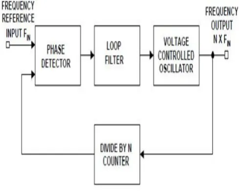
C. Voltage Controlled Oscillator
In the voltage controlled oscillator (VCO), the main part is the multiple stage oscillator which is similar to the ring oscillator. In each stage, there are two PMOS and two NMOS. The upper most PMOS and lower most NMOS operate as current source and the PMOS and NMOS in the middle operate as inverter. The current sources limit the current available to the inverter. Compared with the resistance and capacitance present in the loop filter, the resistance of the VCO should bed resigned infinite and the capacitance of the VCO should be designed smaller.Fig2 shows the standard structure of PLL.
Fig. 2. Standard PLL Structure
IV. DIRECT DIGITAL SYNTHESISER
ISSN(Online): 2320-9801
ISSN (Print): 2320-9798
International Journal of Innovative Research in Computer
and Communication Engineering
(An ISO 3297: 2007 Certified Organization)
Vol. 3, Issue 8, August 2015
Fig. 3. DDS Block Diagram and Waveforms
V. MATLAB-SIMULINK IMPLEMENTATION OF A DIRECT DIGITAL SYNTHESIZER
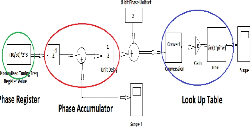
Mat lab-Simulink implementation of a direct digital synthesizer consists of Phase Register (PR), Phase Accumulator (PA) and Look up Table (LUT). Figure 2 shows the system-level model of the DDFS. The PR contains the frequency tuning word. The unit delay block in the Figure 4.1 along with an adder and feedback loop represents the PA. These unit delay blocks act as register. The LUT is implemented using inbuilt sine LUT block of MATLAB-Simulink. The input of the LUT is scaled using the gain block. With every clock pulse the contents of the PR is added to that of PA. The PA generates the phase values of the output sine wave. The output of the PA serves as the address of the LUT. Each time the PA overflows, the LUT outputs sampled values of the sine wave. This output of the LUT represents one cycle of the sine waveform, since the LUT contains sampled values of one cycle of the sine wave. The overflow rate of the PA depends on the bit-size of the PA (number of bits) and the frequency tuning word. Larger the size of the frequency tuning word faster the PA overflows.
ISSN(Online): 2320-9801
ISSN (Print): 2320-9798
International Journal of Innovative Research in Computer
and Communication Engineering
(An ISO 3297: 2007 Certified Organization)
Vol. 3, Issue 8, August 2015
The output frequency of the DDFS is directly proportional to the frequency tuning word. Therefore, larger the frequency tuning word, higher is the output frequency and faster the PA overflows. This is shown with the help of simulations. Both PLL and DDS techniques use digital devices, but the PLL technique is fundamentally analog disciplines. The basic signal generator in both techniques is an oscillator, which is a feedback tuned amplifier set to operate under specific conditions (controlled instability). The oscillator is manipulated to allow the generation of a range of frequencies. In DDS, the signal is generated and manipulated digitally from the ground up, and after all the digital manipulations are completed, it is converted to an analog signal via a digital-to-analog converter.
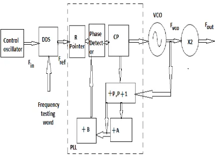
VI. DDS-DRIVEN PLL FREQUENCY SYNTHESIZER
The block diagram of the DDS-driven PLL frequency synthesizer is shown in fig. 5. The reference frequency of DDS, fref, is generated by a crystal oscillator. The output frequency of DDS, fDDS, is controlled by the frequency tuning words. The reference of the PLL is driven by the output of DDS, fDDS. The output of VCO is controlled by the output of Charge Pump (CP) of PLL. The output signal of this frequency synthesizer of obtained by multiplying fvco. The PLL module has a dual-modulus prescaler that has the pulse swallow function. This enables the large division ratio. The dual-modulus prescaler make it possible for the frequency synthesizer to generate higher output frequency while the frequency resolution is improved.
ISSN(Online): 2320-9801
ISSN (Print): 2320-9798
International Journal of Innovative Research in Computer
and Communication Engineering
(An ISO 3297: 2007 Certified Organization)
Vol. 3, Issue 8, August 2015
VII. MODEL EXPLANATION
Phase-locked loop (PLL) is a feedback loop which locks two waveforms with same frequency but shifted in phase. The fundamental use of this loop is in comparing frequencies of two waveforms and then adjusting the frequency of the waveform in the loop to equal the input waveform frequency. Used to synchronize the phase of two signals, the PLL is employed in a wide array of electronic and communications equipment, including microprocessors devices such as radios, televisions, and mobile phones. The basic blocks of the PLL are a phase detector, a low-pass filter, a variable frequency oscillator, and a divider.
A. Pulse Generator
The Pulse Generator block generates the reference signal. It produces a periodic pulse train. The variable synFr denotes the frequency of the pulse train. The period of the pulse train is 1/synFr. To change the value of the period, the value of the variable synFr has to be changed so that the new value of synFr is used in all the blocks whose parameters reference the variable synFr.
B. Divide Frequency subsystems
There are two divide frequency subsystems divide frequency by synM and divide frequency by synN. The divide frequency by synM subsystem divides the frequency of the reference signal by the variable synM. The output of the block is a pulse train called the frequency-divided reference signal. This value determines the step of the output frequency setting. The divide frequency by synN subsystem divides the frequency of the synthesized signal by the variable synN. The output of this subsystem is called the frequency-divided synthesized signal. At steady state its frequency has the same value as the output one of the synM subsystem. The value of the divisor in these subsystems can be changed by changing the value of synM or synN
.
C. Phase Detector
The Logical Operator block acts as a phase detector. It uses the XOR operation to compare the frequencies of the frequency-divided reference signal and the frequency divided synthesized signal. At steady state, the signal is a pulse train with frequency two times higher than the both inputs. The reason for this is that both inputs to the block have equal frequencies, but they are out of phase by 1/4 of their period. As a result, the signal after the XOR operation is a periodic pulse train with double frequency.
D. Analog Filter Design
The Analog Filter Design block filters high frequencies out of the signal coming from the phase detector. The block uses a low pass Butterworth filter. A higher-order filter or another filter type can be used to improve the stability of the synthesized signal. In the steady state of the model, the amplitude of the output signal is approximately constant. This is the average value of the output from the phase detector. A Gain block multiplies the output signal from the Analog Filter Design block by a constant to produce the control signal.
E. Voltage-Controlled Oscillator
ISSN(Online): 2320-9801
ISSN (Print): 2320-9798
International Journal of Innovative Research in Computer
and Communication Engineering
(An ISO 3297: 2007 Certified Organization)
Vol. 3, Issue 8, August 2015
F. Accumulator
The Accumulator subsystem repeatedly adds the constant synM to a cumulative sum. While the sum is less than 1, the output labelled carry is 0. At a time step when the sum becomes greater than or equal to 1, the carry output is 1 and the cumulative sum is reset to its fractional part. The fraction of the time when the carry output is 1 is equal to synM, while the fraction of the time when it is 0 is equal to 1-synM.
G. Divide Frequency
The Divide Frequency subsystem divides the frequency of the synthesized signal by synN when the output of the accumulator subsystem is 0, and divides it by synN+1.
VIII. PERFORMANCE
A DDS has many advantages over its analog counterpart, the phase-locked loop (PLL), including much better frequency agility, improved phase noise, and precise control of the output phase across frequency switching transitions. Disadvantages include spurs due mainly to truncation effects in the NCO, crossing spurs resulting from high order (>1) Nyquist images, and a higher noise floor at large frequency offsets due mainly to the Digital-to-analog converter Because a DDS is a sampled system, in addition to the desired waveform at output frequency Nyquist images are also generated In order to reject these undesired images, a DDS is generally used in conjunction with an analog reconstruction low pass filter.
A. frequency Agility
The output frequency of a DDS is determined by the value stored in the frequency control register (FCR), which in turn controls the NCO's phase accumulator step size. Because the NCO operates in the discrete-time domain, it changes frequency instantaneously at the clock edge coincident with a change in the value stored in the FCR. The DDS output frequency settling time is determined mainly by the phase response of the reconstruction filter. An ideal reconstruction filter with a linear phase response (meaning the output is simply a delayed version of the input signal) would allow instantaneous frequency response at its output because a linear system cannot create frequencies not present at its input.
B. Phase Noise and Jitter
The superior close-in phase noise performance of a DDS stems from the fact that it is a feed-forward system. In a traditional phase locked loop (PLL), the frequency divider in the feedback path acts to multiply the phase noise of the reference oscillator and, within the PLL loop bandwidth, impresses this excess noise onto the VCO output. A DDS on the other hand, reduces the reference clock phase noise by the ratio clock frequency to output frequency because its output is derived by fractional division of the clock. Reference clock jitter translates directly to the output, but this jitter is a smaller percentage of the output period (by the ratio above). Since the maximum output frequency is limited to clock frequency divided by two, the output phase noise at close-in offsets is always at least 6dB below the reference clock phase-noise. At offsets far removed from the carrier, the phase-noise floor of a DDS is determined by the power sum of the DAC quantization noise floor and the reference clock phase noise floor.
VIII. SIMULATION RESULTS
ISSN(Online): 2320-9801
ISSN (Print): 2320-9798
International Journal of Innovative Research in Computer
and Communication Engineering
(An ISO 3297: 2007 Certified Organization)
Vol. 3, Issue 8, August 2015
IX. CONCLUSIONS
The proposed comparative study consists of PLL, DDS and DDS- based PLL. A DDS- driven PLL frequency synthesizer architecture is given in this paper. The result of DDS- based PLL architecture describing the mixed behaviour of this DDS based PLL architecture starting from the specifications of each building block. The HDL models of critical PLL blocks have been described in VHDL-AMS to predict the different specifications of the PLL. The effect of different noise sources has been efficiently introduced to study the system performance. The phase locked loop (PLL) has been widely used in wireless communication systems due to the high frequency resolution and the short locking time. The usage of Direct Digital Synthesis (DDS) avoids some of the typical trade-offs in PLL like the achievement of a very high-frequency resolution together with fast settling and spectral purity. The comparative study showed the performances of different parameters. Finally, DDS- based PLL synthesis technique is better than other techniques.
X. ACKNOWLEDGMENT
The authors would like to thank Prof. Saju A for discussing the concept.
REFERENCES
1. Dan Morelli, “Modulating Direct Digital Synthesizer in a FPGA”, VP of Engineering Accelent System Inc, QuickLogic, pp. 143-156, Feb. 2008. 2. Bar-Giora Goldberg, “Digital Frequency Synthesis Demystified”, 6th Edition, LLH, Publishing Technology, 1999, Ch. 1, pp. 1-12.
3. Govind Singh Patel1 & Sanjay Sharma2 Comparative Study of PLL, DDS and DDS-based PLL SynthesisTechniques for Communication System International Journal of Electronics Engineering, 2(1), 2010, pp. 35-40.
4. Saeed Golestan, Member, IEEE, Francisco D. Freijedo, and Joseph M. Guerrero, Senior Member, IEEE, “A Systematic Approach to Design Higher-Order Phase Locked Loops” IEEE Trans. Power Electronics, 2013.
5. V. F. Kroupa, Direct Digital Frequency Synthesizers. New York: IEEE. 6. D. Banerjee, PLL Performance, Simulation, and Design, Fourth Edition.
7. National Semiconductor, 2006.Moscow, Russia Pascal Nelson, “Design and Analysis Freq. Synthesizers using FPGA as Reconfiguration Hardware”, Analog Devices Inc.(Greensboro, N.C.), EE Times Publication, pp. 45-48, Sept. 2003.
8. B. A. Wittman, S. H. Early, and D. G. Messerschmitt, \A Hardware Multitone Digital Frequency Synthesizer," IEEE Transactions on Acoustics, Speech, and Signal Processing, vol. ASSP-27, pp. 804{809, Dec. 1979.
9. Shashi Kant shrimali, Direct Digital Frequency Synthesizer, thesis, Texas Tech University, May 2007.
ISSN(Online): 2320-9801
ISSN (Print): 2320-9798
International Journal of Innovative Research in Computer
and Communication Engineering
(An ISO 3297: 2007 Certified Organization)
Vol. 3, Issue 8, August 2015
BIOGRAPHY
Ms. Sreelekshmi K. R., received her B. Tech Degree in Electronics & Communication Engineering from Cochin University in 2013. At present she is pursuing M. Tech in
Communication Engineering at Believers Church Caarmel Engg. College, Kerala.
Ms. Subhalekshmi K. R., received her B. Tech Degree in Electronics & Communication Engineering from Cochin University in 2013. At present she is pursuing M. Tech in Communication Engineering at Believers Church Caarmel Engg. College, Kerala.