Design of High Performance Scan Register Insertion on
Integer Arithmetic Cores
[1]
Vootla.Sridhar,
[2]Dr. T.Srinivas
1(
Research scholar(25617100), Dept of ECE, Shri jagadishprasad Jhabarmal Tibrewala Uinversity,
Jhunjhunu,Rajasthan .&
Assistant professor, Dept. Electronic & Communication engineering
Mother Theressa College Of Engg & Tech. Peddapalli, , India
2
professor, Dept. Electronic & Communication engineering
. Peddapalli, , india
E-Mail: [email protected]
1, [email protected]
2ABSTRACT: Insertion of Scan flip–flop for testability invites in aiding design for overhead additional hardware thereby performing the deteriorating of the circuit. In this paper, we shall demonstrate a FPGA based implementation for Finite State Machines in the insertion of scan registers and data path pipelined circuits with no overhead or compromise in performance of the hardware. All our designs which as been proposed have been realized using a low–level design methodology relatively involving target FPGA family based instantiation primitive, coupled with their constrained placement on the fabric Xilinx FPGA. Implementation results clearly reveal the our proposed architectures in superiority comparison to equivalent circuits derived through modelling behavioural with respect to speed and area. Additionally, our proposed scan register rcircuit inserted with circuits designed without compare favourably for scan flip–flops. Coupled with this, lies the ease of an of the corresponding Hardware Description Language (HDL) automated generation and placement constraints and their portability among other FPGA families from advanced Xilinx.
1.INTRODUCTION
Design for testability (DFT) is an essential for enhancing the observability and controllability of a circuit. This often involves replacing the normal flip– flops (FFs) by scan FFs, which addition includes of a multiplexer at the normal the input FFs and the select line decides between the and the test normal mode or scan mode of operation. In the normal mode, the in accordance to the circuit operates functionality specified, while in the scan mode test , the series of FFs are converted into a shift register, through bit sequence which any desired input shifted–in serially through a dedicated scan in pin, or the of the circuit can be read out by entire state shifting out the FF dedicated scan out pin contents .Such circuit modifications invite additional hardware path delay owing to introduction of multiplexers and increase the critical. chain insertion Scan on FPGAs have been studied in [2] and [3], which resulted in previously resource overhead. However, for certain class of circuits, imposed through the limitations additional circuitry can be when such scan mitigated FF inserted circuits are deployed on modern FPGA families, which optimum logic support resources. In order to reap the of the advanced benefits FPGA architectures, it is not sufficient to enter a Register Transfer Level (RTL) behavioural or mode of Hardware Description Language (HDL) at the of the
performance of the circuit inclusive of the DFT functionality matches to the using similar circuit realized principles of and constrained placement primitive instantiation but exclusive of the DFT functionality.
2. SLICE ARCHITECTURE OF XILINX VIRTEX–7 FPGA
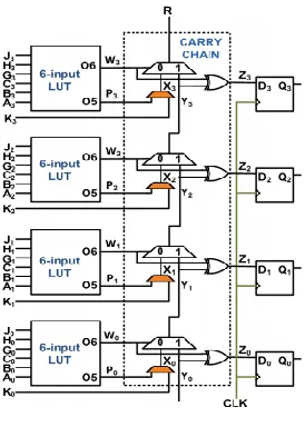
A typical Configurable Logic Block (CLB) of our implementation platform, Virtex–7 FPGA, with each slice (called a “SLICEL” or “SLICEM”) contains 2 slices, comprising of four 6 input LUTs, eight flip– flops (FFs), three, and a carry chain wide function multiplexers [7]. Each LUT present in SLICEL can implement any arbitrary 6–input single output combinational logic, or two 5 (or less)–input (shared) functions, whereas the LUTs in can additionally implement SLICEM memory elements. The carry chain the fast carry represents propagation logic. Each FF can be controlled using the “set/reset”, “clock”, and “clock enable” signals. A typical Virtex–7 slice architecture, depicting only a subset of the above, has been shown in Fig. 1. The shaded multiplexers features mentioned inside the carry chain indicate that they cannot be instantiated or manually configured, only the CAD tool can configure them in accordance with the HDL.
Architecture of Proposed Designs
In this section, we shall present the detailed FPGA architectures of the arithmetic cores as well as their scan FF incorporated versions.
Loadable Bidirectional Resettable Counter
Binary counter, which as a fundamental serves
component of many controlpath implementations,
should the following desirable features of
resettability, loadability, bidirectionality, possess count–enability, and detectability terminal count [8].
Loadable Bidirectional Resettable Counter Realized Through Primitive Instantiation and Constrained Placement:
A counter is a D–FF based Parallel–In Parallel–Out register and an incrementer/decrementer, as shown in Fig. 2. Di = Qi ⊕ (Qi-1 · Qi-2...Q1 · Q0) for an incrementer and Di = Qi ⊕(Qi-1 + Qi-2 + ... + Q1 +
Q0) for a decrementer if i ≥ 1. D0 = Q0 for both incrementer and decrementer. The wide input AND and OR gate for incrementer and decrementer respectively, are realized using the carry chain. The 6–input LUT is configured as Oi = (LD · Qi + LD · EXTi) ⊕ U/D, where the counter counts up if U/D = 0, counts down if U/D = 1, and loads external data if
LD = 1.
The terminal count is detected by the carry output of the most significant carry chain. Each multiplexer of the carry chain computes AND or OR operation as Ri
= Oi · U/D + Oi · Ri-1 where Ri-1 is the previous AND–ed or OR–ed output. This recurrence relation bears resemblance to (1) making it amenable for carry chain implementation. If U/D = 0, Ri = Oi ·
Ri-1 representing AND functionality, and if U/D = 1, Ri
= Oi · 1 + Oi · Ri-1 = Oi + Ri-1, thereby representing OR functionality. Ri = U/D for i = 0. The XOR gates of the carry chain compute the next state of the counter, Di = Oi⊕Ri-1. The architecture utilizes four out of six inputs per LUT, and a single output instead of the dual outputs of the configured LUTs. Thus, an
3.SCAN FF INCORPORATED COUNTER DESIGN REALIZED THROUGH PRIMITIVE
INSTANTIATION AND CONSTRAINED
PLACEMENT:
In this architecture, the counter operates in two different modes: the normal mode and the scan
mode. In the normal mode of operation, the as per the specified counter operates functionality. In the test
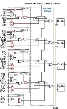
mode, the into the carry chain through a multiplexing arrangement as shown in Fig. 3, and the carry chain fabric is configured to connect all the FFs in a serial– input serial–output (SISO) mode serial data is fed via the LUTs, without disturbing the parallel read–out capability of the counter. This feature serves as an advantage to test other their inputs from the counter. In fact, we present a relevant sub–circuits deriving case study of such a design paradigm in Section V-A. In the architecture depicted in Fig. 3, the O6 and O5 outputs of LUTs compute the following functions:
O6i = TD[(LD · Qi + LD · EXTi) ⊕ U/D] and O5i =
TD · Qi + TD · U/D. Each multiplexer of the carry chain computes Ri = O6i · O5i + O6i · Ri-1, where R0 = TD · U/D + TD · SD. This recurrence relation also bears resemblance to (1) making it amenable for carry chain implementation. Thus, our proposed n–bit
counter with scan FFs occupies n 4 + 1 slices, (n + 1) LUTs and n FFs.
4. Universal Shift Register
Universal Shift Register is a useful data path circuit which has bidirectional shifting and parallel load capabilities.
Universal Shift Register Realized Through Primitive Instantiation and Constrained Placement:
The architecture of the universal shift register is shown in Fig. 4. Two inputs S1 and S0 decide the
operation mode of the registers, and the
combinational logic deciding the functionality can be realized using a 4:1 multiplexer with the options of bidirectional shifting, parallel by directly controlling loading and retaining of previous data as shown in Table I. Additionally, the circuit is also resettable the “reset” input of the FFs. In this architecture, all the six inputs of the LUT are utilized. Thus, an n–bit
circuit occupies n 4 slices, n LUTs and n FFs.
Scan FF Incorporated Universal Shift Register Realized Through Primitive Instantiation and Constrained Placement:
The scan register insertion in Universal Shift Register circuit can be achieved through re–ordering of certain inputs and changing the priority of different
functionalities over one another. This for
original design had already used up all the six inputs of the LUTs. The function corresponding table is depicted in Table II. The “Freeze data” functionality is achieved by connecting has been done to create room an active low signal NC to the clock– enable pin of the D–FF, whereas the input to and test mode of operation for converting the LUT for the left–shift functionality FFs into a scan chain, can be shared. Thus, an n–bit circuit occupies n 4 slices, n LUTs
and n FFs.
Case Study: A Pipelined Two’s Complement Adder– Subtractor Tree
Adder–subtractor tree is a useful sub–circuit that
often finds applications in the parallel
implementation of arithmetic distributed based FIR Filters, matrix multiplication circuits or pipelined binary tree multipliers [9]. Each ADD/SUB block shown in Fig. 6 can configured as a be independently two’s complement adder or subtractor, mode as they have independent select lines. Each of the blocks can
perform a 24–bit two’s complement
addition/subtraction, with a of ADD/SUB blocks. The been re–designed by circuit has total of five stages also inserting scan FFs at the site of the pipeline registers with no hardware and performance deterioration overhead. The slice of a pipelined adder/subtractor tree without the scan configuration FFs have been shown in Fig. 7. The sum bit can be computed by EX–ORing the LUT and carry chain multiplexer output as
Si = Ai ⊕(Bi ⊕ M) ⊕ Ci. The carry output of each
multiplexer stage can be computed as:
Ci+1 = Ai(Bi ⊕ M) + (Ai ⊕ (Bi ⊕ M))Ci
= Ai(Ai(Bi ⊕ M) + Ai(Bi ⊕ M))+(Ai ⊕ Bi ⊕ M)Ci
= Ai(Ai (Bi ⊕ M)) + (Ai ⊕ Bi ⊕ M)Ci
Equation (2) bears resemblance to (1) making it suitable for carry chain implementation. Ci = M for i
= 0. The scan FF inserted pipelined adder–subtractor tree has been shown in Fig. 8. In this circuit, we configure the LUTs in the dual output mode where
O6i = (Ai ⊕ Bi ⊕ M)TD and O5i = Ai · TD + Qi · TD. The carry output of each multiplexer stage is computed as Ci+1 = O6i ·O5i +O6i ·Ci, which bears resemblance to (1), making it suitable for carry chain implementation. C0 = M for normal mode of operation (TD = 0), and C0 = SD for test/scan mode of operation (TD = 1). Since normal mode and scan mode are two non– overlapping operations, the mode input pin receives input during test mode scan–in data of operation. Each of the ADD/SUB blocks have dedicated mode control or serial data input. This allows certain ADD/SUB blocks in the adder tree to operate in the test mode, where any desired bit sequence may be the registers scanned into, which in turn may act as inputs to verify the functionality block operating of another ADD/SUB in the normal
mode, that receives its inputs from those registers.
.
CONCLUSION
We have presented high performance, automated FPGA designs of integer cores arithmetic with scan FFs, following the principle of instantiation primitive and constrained placement. ideally suits The methodology circuits where the configured logic elements are underutilized, or the nature of the circuit in itself permits certain design specific changes such as reshuffling of inputs priority encoding for insertion of scan FFs with no hardware overhead. option settings for any synthesis or optimization goal and effort for the behavioural No amount of changes designs can match up to our proposed architecture, both in terms of speed and area
REFERENCES
[1] M. L. Bushnell and V. D. Agrawal, Essentials of Electronic Testing for Digital, Memory and Mixed-Signal VLSI Circuits. Kluwer Academic Publishers, 2000.
[2] A. Tiwari and K. A. Tomko, “Scan–chain Based Watch–points for Efficient Run–Time Debugging and Verification of FPGA Designs,” in ASP–DAC,
2003, pp. 705–711.
[3] T. Wheeler, P. Graham, B. Nelson, and B. Hutchings, “Using Design– Level Scan to Improve FPGA Design Observability and Controllability for Functional Verification,” in Field–Programmable Logic and Applications, ser. LNCS, vol. 2147, 2001,
pp. 483–492.
[4] A. K. Verma, P. Brisk, and J. P. Ienne, “Challenges in Automatic Optimization of Arithmetic Circuits,” in 19th IEEE International Symposium on
Computer Arithmetic, June 2009, pp. 213–218.
[5] A. Ehliar, “Optimizing Xilinx designs through primitive instantiation,” in Proceedings of the 7th
FPGAworld Conference, 2010, pp. 20–27.
[6] A. Palchaudhuri and R. S. Chakraborty, High Performance Integer Arithmetic Circuit Design on FPGA: Architecture, Implementation and Design
Automation. Springer India, 2015.
[7] Xilinx Inc., “7 Series FPGAs Configurable Logic
Block, UG474 (v1.5)”, Aug. 6 2013. [Online].
Available: http://www.xilinx.com/
support/documentation/user guides/ug474 7Series CLB.pdf
[8] M. R. Stan, A. F. Tenca, and M. D. Ercegovac,
“Long and Fast Up/Down Counters,” IEEE
Transactions on Computers, vol. 47, no. 7, pp. 722–
735, July 1998.
[9] U. Meyer-Baese, “Digital Signal Processing with
Field Programmable Gate Arrays”, 3rd ed. Springer