Almost Periodic Lumped Elements Structure Modeling Using
Iterative Method: Application to Photonic Jets and Planar Lenses
Mohamed Karim Azizi1, *, Henri Baudrand2, Taieb Elbellili1, and Ali Gharsallah1
Abstract—In this work, we show that it is possible to produce a planar electromagnetic jet using a flat structure consisting of elementary cells based on lumped elements and fed with a source line. A combination of elementary cells may represent a gradient index, locating the electromagnetic energy in a small area, consisting of a few cells and having a size of about 0.75λ. The theoretical framework of the study is based on the Wave Concept Iterative Process method (WCIP) formulated in both spectral and spatial domains. An analogy with an optical model based on optical paths equality enables predicting the location of formation of this spot. The use of such a system can provide solutions for the development of new kinds of applications such as engraving sub-wavelength, data storage, improved scalpel optics for ultra-precise laser surgery, and detection of cancer.
1. INTRODUCTION
Several studies have shown that the interaction of an electromagnetic wave with a metallic or dielectric barrier whose shape and dimensions are well defined provides a highly localized scattered light in a small volume of space. This phenomenon is called photonic jet [1, 2]. The high intensity resulting beam spreads with low divergence over a distance of a few wavelengths. It also presents a lower section than the wavelength. This small section of the photon stream, which is not possible to obtain with a “classic” optical device, is an essential characteristic of the jet. Therefore, the photonic jet can be exploited to obtain optic instruments of lower resolutions than the classic resolution limit of λ/2.
To date, several jet photonics-based applications have been considered and implemented for molecules detection [3], optical imaging, data storage [4] and high-resolution microscopy or nonlinear optical effects [5, 6]. Among these applications, most studies and developed applications were based on obtaining a photonic jet from the interaction of an electromagnetic wave with obstacles having spherical [7, 8], cylindrical [9] or elliptic shapes [10, 11], but some of them are interested in producing of planar jets. Other researchers such as Ju and coworkers [12] placed metal under the microcylinder and excited the surface plasmos by a plane wave in order to improve the electromagnetic field by altering the thickness of the micro disk. This enabled the control of nanojets. Some studies have shown that a modification of the geometries of the micro-objects makes it possible to improve the electric field in plasmonic nanojets [13]. Furthermore, various numerical calculation methods have been used to study these systems, such as the finite element method (FEM), method of moments (MOM) and finite-difference time-domain (FDTD) method [14, 15]. FDTD is one of the most used methods thanks to its accurate calculation but still, requires a huge memory space. Moreover, Wave Concept Iterative Process (WCIP) has already shown its effectiveness in solving similar problems in terms of both computing time and calculations accuracy [16]. Thus, we will use the new approach to the iterative method WCIP [17]
Received 19 December 2016, Accepted 8 February 2017, Scheduled 23 March 2017
* Corresponding author: Mohamed Karim Azizi ([email protected]).
1 UR13ES37 Circuits et Syst`emes Electroniques `a Hautes Fr´equences, Facult´e des Sciences de Tunis, Universit´e de Tunis El Manar,
based on technical auxiliary sources to study the phenomenon of the planar jet created by a planar structure of individual cells.
This paper is organized as follows. Section 2 gives a brief presentation of the iterative method WCIP. Section 3 presents the new approach of the method appropriated to almost periodic structures. Section 4, we describe the complete structure which is reviewed by the new approach WCIP. The configuration details are illustrated, and the work is validated compared to the principle of optical paths. In Section 5, a comparison with another method is made taking into account the example of a microstrip bandpass filter design. Section 6 provides simulation results and interpretation of the phenomenon of planar jet. In Section 7, results and discussions are presented. In Section 8, perspectives and conclusions are drawn.
2. PRINCIPLE OF THE WCIP METHOD
The WCIP establishes a recurrence relation between the incident waves and reflected waves in different environments surrounding the discontinuity. It uses the fast Fourier transform in [18] to solve diffraction problems and analyze planar circuits. Unlike various integral methods (moments of methods, differential methods (FDTD) and Finite Element), WCIP does not use the scalar product or matrix inversion. In addition, it allows the study of complexly shaped structures.
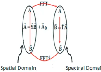
Since the partition of the overall area into two areas leads to an internal/spatial domain (plans localized interfaces or components) and an external/spectral domain, to develop this method, it is necessary to define two dual quantities: current-voltage, -magnetic electric fields, electric field-volume current density.
Under these conditions, the “waves” are defined as:
⎧ ⎪ ⎪ ⎨ ⎪ ⎪ ⎩
A= 1
2√Zo
E+ZoJ
B = 1
2√Zo
E−ZoJ
(1)
Two operators are defined: The first is called S, which deals with the spatial domain and characterizes the boundary conditions; the second is an operator named Γ, which deals with the spectral domain and distinguishes the homogeneous environment.
B = ΓA A=SB+A0
(2)
Rapid Transform Fourier (FFT) and its inverse (FFT−1) provide the translation from one area to another (see Fig. 1).
Figure 1. Schematization of the translation from spatial domain to spectral one and vice versa.
3. NEW APPROACH OF WCIP FOR ALMOST PERIODIC STRUCTURE
This approach is based on the use of auxiliary sources to study almost-periodic structures.
In this kind of periodic structure, defects can be represented by impedances attached to each cell. These impedances are replaced by sources with same dimensions. They are the auxiliary sources. A set of sources can be studied as a superposition of states characterized by sources of the same amplitude, but out of phase with each other and with a constant magnitude. The state’s study is performed on a single cell. This approach is well suited for raking in waves that act as a balance between Spectral areas (outside) and Space (inside or sources). It describes the periodic geometry (outer) space with small irregularities (area sources).
Thanks to almost periodic circuits using auxiliary sources technique, handling with elementary cells becomes easier and helps to achieve multiple applications such as lenses based metamaterials [20] and planar jets. Through this new approach of WCIP which uses V and I as the dual quantities using lumped element, the whole study will be done on one unit cell periodicity view of the walls that surround it. The migration between a cell and another is through two well-defined phases shifted in both directions. The cell is described by impedance seen by “Auxiliary” sources [21]. The auxiliary sources are phase shifted together; the impedances from the spectral domain FFT gives the impedances in each cell (Matrix S). The different states form a basis of which the inverse Fourier transform gives the cells in the spatial domain. Auxiliary sources are used to separate the spatial domain from the spectral range.
4. DETERMINATION OF DIFFRACTION MATRIX OF THE ELEMENTARY CELL AND APPLICATION OF THE WCIP
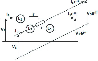
To study the elementary cell, we present the details of the cell composed of auxiliary sources and resistors; this cell is surrounded by periodic walls. For our application, we can simplify the elementary cell [22], and the cell is then represented as follows in Fig. 2; the auxiliary sources E1, E3, E5 will be
replaced by impedances.
Figure 2. Schematic representation of a Cell: The equivalent diagram.
Sources E1, E3 and E5 rely upon electric walls so as to have an alternative current. If they rely
upon magnetic and periodic walls, the current will have a zero value. We have 8 equations and 8 unknowns:
V2=V4 = E5 (3)
I1+I2+I3+I4+I5 = 0 (4)
V1+E1−rI1−E5 = 0 (5)
V3+E3−rI3−E5 = 0 (6)
With the four equations for periodicity:
V2 = V1ejα (7)
V4 = V3ejβ (9)
I4 = −I2ejβ (10)
whereα = 2πmdD represents the phase shift from one cell to the next one in the direction of X, with m
the number of cell, dthe length of cell andDthe length of the structure, and β = 2πndD represents the phase shift from one cell to the next one in the direction ofY.
Rewrite these equations by eliminatingV2,I2,V4,I4:
I1
1−ejα +I3
1−ejβ
+I5 = 5
V1ejα =V3ejβ =E5
(11)
V1
1−ejα +E1−rI1 = 0 V3
1−ejα +E3−rI3 = 0
(12)
These two equations are written as:
E5e−jα
1−ejα +E1 =rI1
E5e−jβ
1−ejβ
+E3 =rI3
−rI1
1−ejα −rI3
1−ejβ
=rI5
(13)
Write Eq. (13) in a compact form:
a=e−jα1−ejα
b=e−jβ
1−ejβ
. (14)
These equations then become:
f I1 I3 I4 =
1 0 a
0 1 b
a∗ b∗ |a|2+|b|2 E1 E3 E5 . (15)
It is now necessary to proceed to the calculation of the eigenvalues in order to determine the reflection coefficient.
The Z matrix is represented by Equation (16). We must now compute the eigenvalues λ of the
matrix
1−λ 0 a
0 1−λ b a∗ b∗ |a|2+|b|2−λ
(16)
which we write:
(1−λ)(1−λ)|a|2+|b|2−λ − |b|2− |a|2(1−λ) = 0 (17) (1−λ)2|a|2+|b|2−λ −(1−λ)|a|2+|b|2 = 0 (18) (1−λ)λ−1 +λ− |a|2+|b|2 = 0 (19) From Equation (25) we can see the existence of 3 eigenvalues:
λ= 0; λ= 1 et λ= 1 +|a|2+|b|2.
We now pass to the calculation of the eigenvectors related to these eigenvalues.
1st case: λ= 0
1 0 a
0 1 b
a∗ b∗ |a|2+|b|2 V1 x Vy1 Vz1
This amounts to writing the following three equations
Vx1+aVz1 = 0 Vy1+bVz1 = 0 a∗Vx1+b∗Vy1+|a|2+|b|2 Vz1 = 0
. (21)
So the first eigenvector isV1 = (
a b
−1 )
2nd case: λ= 1
The equations for the eigenvector forλ= 1 are:
0 0 a
0 0 b
a∗ b∗ |a|2+|b|2−1
Vx2 Vy2 Vz2
= 0. (22)
Equation (22) allows us to write:
aVz2 = 0 bVz2 = 0 a∗Vx2+b∗Vy2+
|a|2+|b|2−1 Vz2 = 0
(23)
So the second proper vector is
V2 =
− b∗ a∗ 0 . (24)
3rd case: λ= 1 +|a|2+|b|2
The equations for the eigenvector forλ= 1 +|a|2+|b|2 are:
−|a|2− |b|2 0 a
0 −|a|2− |b|2 b
a∗ b∗ −1
Vx3 Vy3 Vz3
= 0 (25)
Equation (25) allow us to write:
−|a|+|b|2 Vx3+aVz3 = 0
−|a|+|b|2 Vy3+bVz3 = 0 a∗Vx3+b∗Vy3−Vz3 = 0
(26)
So the third eigenvector is
V3 =
⎛ ⎜ ⎝
a
|a|2+|b|2 b
|a|2+|b|2
1
⎞ ⎟
⎠. (27)
We note that the base V is orthogonal and that it is a normed basis. The vectorsX,Y andZ are the vectors of the orthonormal basis.
X(λ=0)= ⎛ ⎜ ⎜ ⎜ ⎝ a √
|a|2+|b|2 b
√
|a|2+|b|2
−1
√
|a|2+|b|2 ⎞ ⎟ ⎟ ⎟
⎠; Y(λ=1)= ⎛ ⎜ ⎜ ⎝
−b∗
√
|a|2+|b|2+1 a∗
√
|a|2+|b|2+1
0
⎞ ⎟ ⎟
⎠; Z(λ=1+|a|2+|b|2)= ⎛ ⎜ ⎜ ⎜ ⎜ ⎝ a √
|a|2+|b|2∗√|a|2+|b|2+1 b
√
|a|2+√|b|2∗√|a|2+|b|2+1
|a|2+|b|2
√
|a|2+|b|2∗√|a|2+|b|2+1 ⎞ ⎟ ⎟ ⎟ ⎟ ⎠
We are now looking for the admittance matrix:
¯ ¯Y = 1
r
And from this we can deduce
Γ = 1−Z0¯¯Y 1 +Z0¯¯Y
(29)
withZ0: Reference impedance
1 + Z0
r
Y Y+1 +|a|2+|b|2 ZZ+
−1
= 1 +αY Y++βZZ+ (30)
1 +αY Y++βZZ+ 1 + Z0
r Y Y
++Z0 r
1 +|a|2+|b|2
ZZ+
= 1 (31)
α+Z0
r +α Z0
r
Y Y++
β+Z0
r
1 +|a|2+|b|2
+βZ0 r
1 +|a|2+|b|2
ZZ+= 0 (32)
withα= − Z0
r
1+Zr0 and β =
−Z0
r (1+|a|2+|b|2)
1+Zr0(1+|a|2+|b|2).
To find Γ, we multiply Equation (32) by (1−Z0¯¯Y)
Γ = 1 +αY Y++βZZ+ 1− Z0
r Y Y
+−Z0 r
1 +|a|2+|b|2 ZZ+
(33)
Γ = 1 +
α−Z0
r −α Z0
r )Y Y ++
β−Z0
r
1 +|a|2+|b|2
(1 +β)
ZZ+
(34)
Γ = 1 +
− Zr0
1 +Zr0 −
Z0 r +
Z0 r
2
1 +Zr0
Y Y++
−
Z0 r c
1 +Zr0 c − Z0 r c+ Z0 r 2 c2
1 +Zr0 c
ZZ+ (35)
withc= 1 +|a|2+|b|2. Thus Γ = 1− 2
Z0 r
1+Zr0Y Y
+− 2Zr0(1+|a|2+|b|2)
1+Zr0(1+|a|2+|b2)ZZ +.
Whenr tends to 0, we will have:
Γ = 1−2Y Y+−2ZZ+ (36) The next step is just to write the spatial domain conditions.
For theS matrix, we have
S =
−1 short circuit 1 open circuit
Once parameters Γ and S are determined, we can apply the iterative process [23] using these equations
B = ΓA A=SB+A0
(37)
By reaching the convergence, we can calculate theEz field over the whole structure.
5. COMPARISON WITH OTHER METHOD: EXAMPLE OF MICROSTRIP BANDPASS FILTER DESIGN
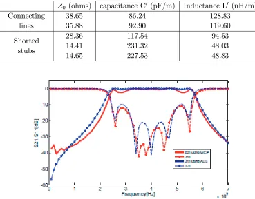
Before proceeding to the main structure of our study, we conduct a comparison of our calculation results with those obtained by the ADS method in the case of the study of a microstrip bandpass structure (Figure 3). The microstrip line has a length ofλ/4 at the midband frequency 4 GHz and a characteristic impedance of 50 ohm. The quarter wave length transmission line sections are discretised on pixel which represents an L-C elementary unit cell as shown in Figure 3.
All the sections of the bandpass filter have a quarter wave length at the midband frequency 4 GHz but with different characteristic impedances which give the values of inductance and capacitance per unit length of a unit cell in every each section as shown in Table 1.
Figure 3. A short circuited stubs bandpass filter layout.
Table 1. Values of the per unit length inductance and per unit length capacitance according to the characteristic impedance.
Z0 (ohms) capacitance C (pF/m) Inductance L (nH/m)
Connecting lines
38.65 35.88
86.24 92.90
128.83 119.60
Shorted stubs
28.36 14.41 14.65
117.54 231.32 227.53
94.53 48.03 48.83
Figure 4. Return loss and transmission loss: Comparison between results of WCIP and ADS.
6. COMPLETE STRUCTURE OF THE PLANAR JET
The structure of the planar jet (133∗140 cells) is shown in Figure 5. The source cells are placed over the entire dumpD of the structure, and x = 0 are supplied in Z. x =x0, placing a thick lens whose
indexn(y) varies in theY direction and is constant in the direction X. The structure is completed in
x =xmax by charging cells. The corresponding cells at y= 0 and ymax represent magnetic walls. The
frequency of simulation isF = 3 GHz. All other cells used throughout the structure are elementary cells which exhibit an index n= 1.
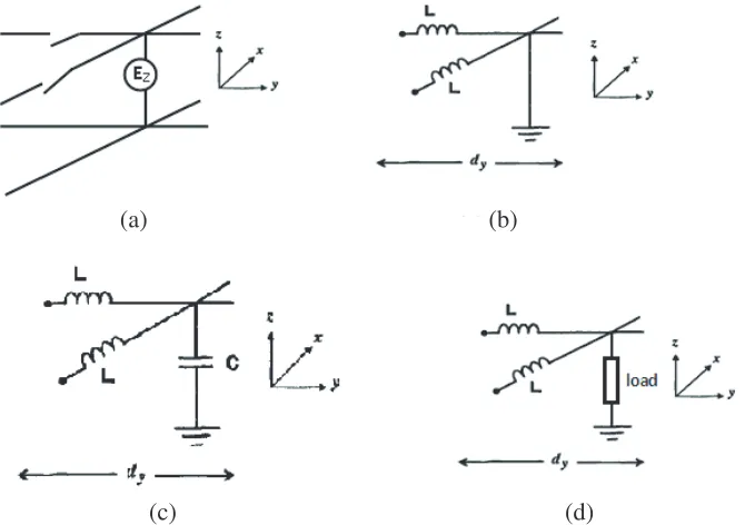
In this configuration, the circuits that form the source cells, unit cells, cells of magnetic walls and expenses cells are shown in Figure 6.
The values of L and C determine the values of μ and ε. We can write that the index is equal to
n=
ε ε0 =
√
Figure 5. Structure of Planar Jet. Red dots represent the source cells and black ones the adapted charge cells. The whole structure is surrounded by magnetic wall cells.
(a) (b)
(c) (d)
Figure 6. Circuits representing the different types of used cells: (a) Source Cell, (b) electric Wall, (c) elementary Cell, (d) charged Cell.
δlis the length of the unit cell. The capacitance per unit length is equal toC = Cδl.
L= L
δl
√
LC =√μ0ε0εr
It is assumed thatμ=μ0 then
n=√εr =
LC μ0ε0
= 1
δl
LC μ0ε0
= C
δl
√
LC (39)
C = 3.108 m/s. Let C0 and L0 values give n = 1. It is assumed that the characteristic impedance of the line is equal to 120 π.
L0
C0 =
μ0
ε0, where
√
L0C0 =
√
μ0ε0δl, takingεr= 1 we find n= 1.
n= C
δl
L0C0 = C δl
√
μ0ε0δl= 1
Then
L0 C0
L0C0 =L0 =
μ0 ε0
√
μ0ε0δl=μ0δl
(40)
Similarly, in the following, we will setLto L0, while C varies.
With an indexn, we have
C=C0n2 (41)
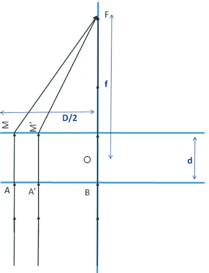
Figure 7 represents the equivalent optical system under study, based on the equality of optical paths, by considering a ray passing through the center of the lens and its optical path and by comparing with that of another ray passing through the lens.
Figure 7. Optical system equivalent to the system studied. Incident beam from infinity (parallel rays) on a flat lens with a variable longitudinal refractive indexs.
The equality of optical paths requires:
BO+OF =d∗n0+f =AM +M F =d∗n
D
2
+
f2+ D2
4
At any point A to be ordered:
d∗n(0) +f =d∗n(y) +(f2+y2)
then n0−n(y) =
1
d∗
(f2+y2)−f (43)
d=(f2+y2)−f (44)
7. RESULTS AND DISCUSSIONS
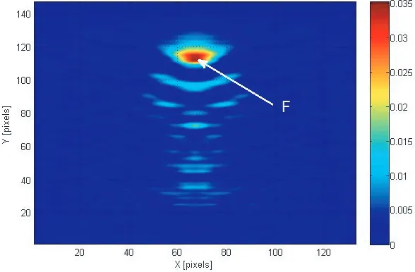
Figure 8 represents the distribution of the field intensity in the area calculated for a compound of structure (133×147 pixels) wherein the thickness of the lens is d = 20 pixels. A strong localization of the field is noted on a small area at a distance of 114 pixels from the source line. According to the width D of 133 pixels of our structure and the chosen value d= 20 pixels from the lens, the previous calculations (Equation (10)) show that this position corresponds to the focus F of the lens. Our system, therefore, has a focal lengthf = 4.9λ.
Figure 8. Electric field intensity mapping. The planar jet shows a maximum intensity at F (focus).
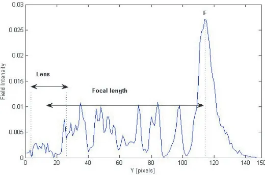
Figure 9 is the field strength along the line of pixels through the focus F. It is seen that the curve is symmetrical. Theoretically, the focal length is at the 67th cell which represents the center of the structure, and the simulated focal length is the same as the calculated one. The full width at half maximum (FWHM) of the spot is about 0.75λ.
Figure 10 represents the distribution of the intensity of the electromagnetic field along the propagation axis y and shows a maximum at y = 114 equivalent to 4.9λ from the center of the lens, representing the focusing point F in Figure 8. The distance of the focal length obtained in the simulation is the same as that found in the calculation. This result confirms the efficiency and precision of the method for planar and optical applications.
Figure 9. Electromagnetic field intensity along the transverse axis.
Figure 10. Intensity distribution of the electromagnetic field along the propagation axisx.
8. CONCLUSION
A new approach of the WCIP method has been applied to a planar structure composed of a flat lens in order to study the electromagnetic jet phenomenon. This approach has shown its efficiency in terms of precision, and the iterative process converges faster than the FEM simulations. A good agreement between the calculated focal values and that found following simulations is obtained.
WCIP method can be applied to other applications with more complicated design circuits. The study and modeling of metasurfaces and structures based on graphene will be our future work.
REFERENCES
1. Chen, Z., A. Taflove, and V. Backman, “Photonic nanojet enhancement of backscattering of light by nanoparticles: A potential novel visible-light ultramicroscopy technique,”Opt. Express, Vol. 12, No. 7, 1214–1220, 2004.
2. Kim, M.-S., T. Scharf, S. M¨uhlig, C. Rockstuhl, and H. P. Herzig, “Engineering photonic nanojets,”
Opt. Express, Vol. 19, No. 11, 10206, 2011.
virtual imaging at 50 nm lateral resolution with a white-light nanoscope,” Nat. Commun., Vol. 2, 218, 2011.
4. Dantham, V. R., P. B. Bisht, and C. K. R. Namboodiri, “Enhancement of Raman scattering by two orders of magnitude using photonic nanojet of a microsphere,” Journal of Applied Physics, Vol. 109, No. 10, 2011.
5. Kong, S.-C., A. Sahakian, A. Taflove, and V. Backman, “Photonic nanojet-enabled optical data storage,” Opt. Express, Vol. 16, No. 18, 13713, 2008.
6. Heifetz, A., S. C. Kong, A. V. Sahakian, A. Taflove, and V. Backman, “Photonic nanojets,”Journal of Computational and Theoretical Nanoscience, Vol. 6, No. 9, 1979–1992, 2009.
7. Chen, Z., A. Taflove, and V. Backman, “Photonic nanojet enhancement of backscattering of light by nanoparticles: A potential novel visible-light ultramicroscopy technique,”Opt. Express, Vol. 12, No. 7, 1214–1220, 2004.
8. Li, X., Z. Chen, A. Taflove, and V. Backman, “Optical analysis of nanoparticles via enhanced backscattering facilitated by 3-D photonic nanojets,”Opt. Express, Vol. 13, No. 2, 526–533, 2005. 9. Lecler, S., Y. Takakura, and P. Meyrueis, “Properties of a three-dimensional photonic jet,” Opt.
Lett., Vol. 30, No. 19, 2641–2643, 2005.
10. Itagi, A. V and W. A. Challener, “Optics of photonic nanojets,”J. Opt. Soc. Am. A. Opt. Image Sci. Vis., Vol. 22, No. 12, 2847–58, 2005.
11. Ammar, N., T. Aguili, H. Baudrand, B. Sauviac, and B. Ounnas, “Wave concept iterative process method for electromagnetic or photonic jets: Numerical and experimental results,” IEEE Transactions on Antennas and Propagation, Vol. 63, No. 11, 1, 2015.
12. Ju, D., H. Pei, Y. Jiang, and X. Sun, “Controllable and enhanced nanojet effects excited by surface plasmon polariton,” Appl. Phys. Lett., Vol. 102, 171109, 2013.
13. Khaleque, A. and Z. Li, “Tailoring the properties of photonic nanojets by changing the material and geometry of the concentrator,” Progress In Electromagnetics Research Letters, Vol. 48, 7–13, 2014.
14. Chen, Z., X. Li, A. Taflove, and V. Backman, “Backscattering enhancement of light by nanoparticles positioned in localized optical intensity peaks,”Appl. Opt., Vol. 45, No. 4, 633–638, 2006.
15. Godi, G., R. Sauleau, and D. Thouroude, “Performance of reduced size substrate lens antennas for millimeter-wave communications,” IEEE Trans. Antennas Propag., Vol. 53, No. 4, 1278–1286, 2005.
16. Boriskin, A. V., A. Rolland, R. Sauleau, and A. I. Nosich, “Assessment of FDTD accuracy in the compact hemielliptic dielectric lens antenna analysis,” IEEE Trans. Antennas Propag., Vol. 56, No. 3, 758–764, 2008.
17. Azizi, M. K., N. Sboui, F. Choubani, and A. Gharsallah, “A novel design of photonic band gap by F.W.C.I.P method,”2008 2nd International Conference on Signals, Circuits and Systems, SCS 2008, 2008.
18. Latrach, L., M. Karim Azizi, A. Gharsallah, and H. Baudrand, “Study of one dimensional almost periodic structureusing a novel WCIP method,”International Journal on Communications Antenna and Propagation (I.Re.C.A.P.), Vol. 4, No. 6, December 2014, ISSN 2039–5086.
19. Baudrand, H. and R. S. N’gongo, “Applications of wave concept iterative procedure,”Recent Res. Devel. Microwave Theory Tech., Vol. 1, 187–197, 1999.
20. Pendry, J. B., A. J. Holden, D. J. Robbins, and W. J. Stewart, “Magnetism from conductors and enhanced nonlinear phenomena,” IEEE Trans. Microw. Theory Tech., Vol. 47, No. 11, 2075–2084, 1999.
21. Baudrand, H., M. K. Azizi, and M. Titaouine, General Principles of the Wave Concept Iterative Process, 1–42, John Wiley & Sons, Inc, September 2016.