Ultra-Compact Metamaterial Absorber with Low-Permittivity
Dielectric Substrate
Haibin Sun1, Yongjun Huang1, *, Jian Li1, Weiren Zhu2, and Guangjun Wen1
Abstract—We analyze and discuss an ultra-compact metamaterial absorber (MA) by introducing meander lines into the resonant cells and covering another dielectric layer onto the MA. The size reduction procedures are presented step by step and an ultra-compact metamaterial absorber with in-plane (lateral) dimension of λ/28 and vertical thickness of λ/37 is obtained. We further present two variations of MA configurations which can reach similar compact sizes. The proposed ultra-compact MAs show near-unity absorption under a wide range of incident angles for both TE and TM radiations.
1. INTRODUCTION
In recent years, planar artificial structured materials, known as planar metamaterials or metasurfaces [1– 3], have received exciting research interests due to their ultra-thin vertical sizes, and flexible controllability of the polarization direction and magnitude/phase for both transmitted and reflected electromagnetic/optical waves. One of the most significant applications of planar metamaterials can be found widely in the well-developed chiral metamaterials, whose optical activity can be extremely amplified within a very limited thickness [4, 5]. Another application is the perfect absorption proposed in 2008 by Landy et al. [6] and Tao et al. [7]. Two families of metamaterial absorber (MA) configurations (with and without ground planes) are then quickly developed based on these two pioneering works. These metamaterial absorbers can operate at almost arbitrary frequency spectra ranged from radio frequencies, microwave and terahertz frequencies, to even optical frequencies [8–13]. Moreover, strategies for expanding the operating bandwidths of MAs, such as dual-band [14, 15], triple-band [16, 17], multi-band [18, 19], multi-band-tunable [20, 21], broad-multi-band [22, 23], and ultra-broad-multi-band [24, 25] designs, have also been reported in recent years. Simultaneously, the theoretical analysis methods including classic electromagnetic theory [7], interference theory [26], and equivalent circuit/transmission line theory [27] are developed to analyze and guide the design procedures and explain the appeared exciting absorbing properties.
As mentioned above, almost all the MAs exhibit very thin vertical sizes, and the basic units of MAs also have very compact sizes compared to the operating wavelengths. However, for some specific applications (for examples, integrating into compact antennas/array or microwave integrated circuits for the purpose of reducing the coupling between adjacent elements), one needs ultra-compact embedding media so that they can be considered as fully homogenized media and will not induce side effects in the whole system. Quite recently, two works are reported to achieve ultra-compact MAs by using a substrate of high dielectric constant [28] and a two-layer design [29]. The former one uses a substrate with relative permittivityr= 100 which is of high-cost and difficult to be fabricated in practical. Most importantly,
Received 24 December 2014, Accepted 22 January 2015, Scheduled 29 January 2015 * Corresponding author: Yongjun Huang (yongjunh@uestc.edu.cn).
1 Centre for RFIC and System Technology, School of Communication and Information Engineering, University of Electronic Science
and Technology of China, Chengdu 611731, China. 2 Advanced Computing and Simulation Laboratory (AcL), Department of
the antennas/array or other components deposed on such a substrate may also be affected by its high permittivity and not work properly. The two-layer design requires two different substrates and needs metallic holes for inter-layer connections of metallic lines and patches, which raises the complexity in practical fabrications. Especially at higher frequencies, metallic holes are difficult to be fabricated using a standard printed circuit board (PCB) process.
In this paper, we propose a very simple and easy-to-fabricate procedure to achieve ultra-compact sized MAs with low dielectric constant substrate. Specifically, based on a side-by-side split ring resonator, by introducing bending meander lines within the rings, reducing the period space while keeping the resonator’s size, adding a cover layer, and finally detuning the thicknesses of the substrate, near-unity absorptions can be achieved easily. All of the above mentioned procedures are able to reduce the electric size of the MA unit cell, and therefore an ultra-compact MA can be realized.
2. STEP BY STEP REDUCTION OF THE ELECTRIC SIZE
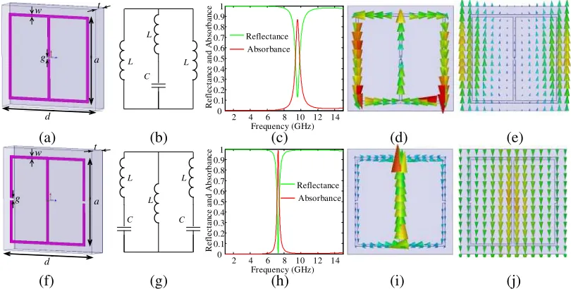
We start by briefly reviewing the absorption properties of two kinds of MA configurations in the microwave frequency region as concluded in Fig. 1. Such two MA configurations were discussed previously [6, 30], and the corresponding metamaterial units, the electric-LC (ELC) resonators, were also analyzed comparatively [31], which shows that the side-by-side split ring resonator [Fig. 1(f)] has lower operating frequency compared to the classic one [Fig. 1(a)] of the same size. This is because these two resonators have equivalent circuits as shown in Figs. 1(b) and (g), and their resonance frequencies areω0=
3/(LC), andω0 =3/(2LC). Therefore, the side-by-side split ring resonator based MA has a lower absorbing frequency as shown in Figs. 1(c) and (h). In other words, the side-by-side inclusion has smaller unit size when operating at a given frequency. Here, a conventional low dielectric constant substrate (FR4 with permittivityr= 4.4 and loss tangent tanδ= 0.02) with thickness oftis used for all the discussions in this paper. The thickness of the metallic (copper with conductivity of 5.8×10⁷S/m) resonator and ground plane is 0.017 mm. The dimensional parameters of the unit cell are chosen to be
a= 3.4 mm, d= 4 mm,g=w= 0.1 mm, andt= 0.8 mm, for both MA configurations. The reflectance and absorbance spectra of both MAs are shown in Fig. 1. At the same time, the surface current distributions on the metallic resonators and ground planes for the two MA configurations are plotted in
d
a
w t
g
d
a
w t
g
2 4 6 8 10 12 14 0
0.1 0.2 0.3 0.4 0.5 0.6 0.7 0.8 0.9 1
Frequency (GHz)
Ref
lect
a
n
c
e
an
d
A
b
so
rb
an
ce
Reflectance Absorbance
2 4 6 8 10 12 14 0
0.1 0.2 0.3 0.4 0.5 0.6 0.7 0.8 0.9 1
Frequency (GHz)
Ref
lect
a
n
c
e
an
d
A
b
so
rb
an
ce
Reflectance Absorbance
C L L
L L
C L
C L
(a) (b) (c) (d) (e)
(f) (g) (h) (i) (j)
Figs. 1(d), (e) and (i), (j). It is indicated that stronger electric fields are located in the outside region for the side-by-side resonator, so the mutual coupling between adjacent resonators becomes stronger, and thus, the absorbing frequency decreases. This is more significant when the periodicity of the MA is small, which will be discussed later. Therefore, in this paper, we choose the side-by-side split ring resonator as the basic MA unit, and all the following discussions are based on this kind of resonator.
We first add meander lines within the resonators while keep the outer ring size fixed to decrease the operating frequency of the MA (equivalent to reduce the electric size for a given frequency). The meander lines technique has been widely used in the engineer area for reducing the electric size of antennas or microwave circuit components, as well as reducing the electric size of metamaterial units [32, 33]. Here we gradually add the meander lines to see the decreases of the absorbing frequency. As shown in Fig. 2(a), there are maximum seven obtainable meander lines for our chosen resonator with the line width of 0.1 mm and space of 0.1 mm between two lines. Therefore, we modeled all the conditions with different orders of meander lines and show the result in Fig. 2(b). It is seen that, with the increase of meander line orders, the absorbing frequency red-shifts gradually, and the absorption strength is also reduced. This is because with additional meander line orders, the equivalent electric length and thus the self-inductor of the resonator increase. Therefore, the resonance frequency decreases rapidly. At the same time, the equivalent impedance [27] of the MA also changes to inductive domain, and the MA becomes impedance mismatch to the background space. It should be noted that before we get the final MA size, we do not focus on the impedance match because it is easy to be realized by changing the substrate thickness which will be performed later.
We then gradually reduce the periodicity of the MA from 4 mm to 3.5 mm by a step of 0.1 mm. Fig. 3(a) shows that the absorbing frequency further shifts to lower frequency gradually as the periodicity reduces. This is because when reducing the period space, the mutual couplings between adjacent resonators will be enlarged, and as a result, both the mutual capacitance and inductance increase. And we know that the increase of mutual capacitance acts as the main contribution due to the outside splits of our chose resonators. At the same time, from Fig. 3(a) we know that the absorbing strength increases. This is because both the added mutual capacitance and inductance are parallel to the self-capacitance and inductance [34]. As a result, the total capacitance increases, and contrarily the total inductance decreases, so the whole system shows less inductive.
Next, we try to add a cover layer (also the FR4 dielectric layer) on the MA in front of the metallic resonator with different thicknesses to continuously reduce the absorbing frequency. Our previous researches [20, 21] show that the added cover layer would contribute to decreasing the operating frequency. As shown in Fig. 3(b), a moderate reduction of the absorbing frequency is clearly indicated. This is because the added cover makes a higher background dielectric permittivity around the metallic resonator. However, it cannot decrease the absorbing frequency unlimitedly by increasing the thickness of the cover layer. As can be seen, when the thickness of cover layer increases to 0.5 mm, the absorbing frequency shift is quite small compared with the initial conditions of 0.1 mm or 0.2 mm.
1 2 3 4 5 6 7 8 9 10
0 0.1 0.2 0.3 0.4 0.5 0.6 0.7 0.8 0.9 1
N=0 N=1 N=2 N=3 N=4 N=5 N=6 N=7
Frequency (GHz)
Ab
so
rb
a
n
c
e
N=0
N=4
N=1
N=5
N=2
N=6
N=3
N=7
(a) (b)
1 2 3 4 5 6 0
0.1 0.2 0.3 0.4 0.5
d=4.0 mm
d=3.9 mm
d=3.8 mm
d=3.7 mm
d=3.6 mm
d=3.5 mm
Frequency (GHz)
A
b
so
rb
an
ce
1 1.5 2 2.5 3 3.5 4 4.5 5 0
0.1 0.2 0.3 0.4 0.5
t'=0.0 mm
t'=0.1 mm
t'=0.2 mm
t'=0.3 mm
t'=0.4 mm
t'=0.5 mm
A
b
so
rb
an
ce
(a) (b)
Frequency (GHz)
Figure 3. (a) The absorbance properties of meandered MAs with different period spaces, and (b) the absorbance properties of meandered MAs with smallest period space and added dielectric cover with different thicknesses.
1 1.5 2 2.5 3 3.5 4 4.5 5 0
0.1 0.2 0.3 0.4 0.5 0.6 0.7 0.8 0.9 1
t=0.8 mm
t=0.9 mm
t=1.1 mm
t=1.3 mm
t=1.5 mm
Frequency (GHz)
A
b
so
rb
an
ce
1 1.5 2 2.5 3 3.5 4 4.5 5 0
0.1 0.2 0.3 0.4 0.5 0.6 0.7 0.8 0.9 1
t=1.7 mm
t=1.9 mm
t=2.1 mm
t=2.3 mm
t=2.5 mm
Frequency (GHz)
A
b
so
rb
an
ce
(a) (b)
Figure 4. The final ultra-compact MA with different substrate thickness to achieve near-unity absorbance.
Now the target absorbing frequency has reached to 3.2 GHz, a relatively low operating frequency compared with the classic configuration which operated near 9.6 GHz [see Fig. 1(c)]. Finally, we detune the substrate thickness [7] to refine the perfect impedance match and so the near-unity absorption. As shown in Fig. 4, when gradually increasing the substrate thickness from the original 0.8 mm to 2.5 mm, the peak absorbing strength first increases to near-unity at condition of t = 2.1 mm and then drops down when further increasing the thickness. Meanwhile, when increasing the substrate thickness, a slight red-shift of the resonant frequency is obtained. Finally, we get the optimized design for our ultra-compact MA with dimensional parameter of a = 3.4 mm, d= 3.5 mm, g =w = 0.1 mm, t = 0.5 mm,
t= 2.1 mm, andN = 7. The final near-unity absorbing peak (99.92%) is located at 3.1 GHz. Therefore, the unit cell size is only 1/28 of the operating free space wavelength.
Table 1. The concluded ultra-compact MA characteristics for different designs.
Works r Physical Period Absorbing Frequency Electric Period
Cao et al. [28] 100 7.2 mm 1.264 GHz 1/33
Lin et al. [29] 4.4 3.1 mm 0.282 GHz 1/39
Design 1 4.4 3.5 mm 3.10 GHz 1/28
Design 2 4.4 3.5 mm 2.79 GHz 1/31
Design 3 4.4 3.5 mm 2.30 GHz 1/37
3. DISCUSSIONS
Here we first discuss the absorbing abilities of our optimized MA at wide incidence angles for both TE and TM radiations. As shown in Fig. 5, our ultra-compact MA can absorb incident electromagnetic waves at a wide range of incident angles. Especially, for the TE radiation, the peak absorbance of 99.92% is obtained at normal incidence and remains greater than 93.95% when the incident angle reach to even 80◦. For the case of TM radiation, the absorption also remains greater than 93.72% for all angles of incidence ranging from 0◦ to 80◦. The very high absorption strength for all incidence angles and the near-same absorption properties for the TE and TM radiations indicate that the proposed MA has very good absorption ability, due to the ultra-compact configurations.
In the above, we demonstrate that introducing meander lines into the MA has shown a significant decrease of the operating frequency. Here we further discuss other two types of meander lines configurations using the same step-by-step procedures to get the optimized ultra-compact MA designs. As shown in Fig. 6, two new meander lines configurations also indicate quite low absorbing frequencies
3 3.1 3.2 3.3 3.4 3.5
0 0.1 0.2 0.3 0.4 0.5 0.6 0.7 0.8 0.9 1 Frequency (GHz) A b so rb an ce
1 1.5 2 2.5 3 3.5 4 4.5 5
0 0.1 0.2 0.3 0.4 0.5 0.6 0.7 0.8 0.9 1 0° 10° 20° 30° 40° 50° 60° 70° 80° Frequency (GHz) A b so rb an ce k H E
1 1.5 2 2.5 3 3.5 4 4.5 5
0 0.1 0.2 0.3 0.4 0.5 0.6 0.7 0.8 0.9 1 0° 10° 20° 30° 40° 50° 60° 70° 80° k E H Frequency (GHz) A b so rb an ce
3 3.1 3.2 3.3 3.4 3.5
0 0.1 0.2 0.3 0.4 0.5 0.6 0.7 0.8 0.9 1 Frequency (GHz) A b so rb an ce (a) (b) (c) (d)
1 1.5 2 2.5 3 3.5 4 0
0.1 0.2 0.3 0.4 0.5 0.6 0.7 0.8 0.9 1
Frequency (GHz)
Ref
lect
a
n
c
e
an
d
A
b
so
rb
an
ce
1 1.5 2 2.5 3 3.5 4 0
0.1 0.2 0.3 0.4 0.5 0.6 0.7 0.8 0.9 1
Frequency (GHz)
R
e
fl
e
c
ta
nc
e
a
n
d
A
b
so
rb
a
n
c
e
Reflectance Absorbance
Reflectance Absorbance
(a) (b)
Figure 6. The absorbance properties for other two meandered variations of the super compact MAs.
(2.79 GHz and 2.30 GHz for these two designs, respectively). It should be noted that, at lower absorbing frequency, a thicker substrate is required to keep near-unity absorption strength. Typically, the overall thicknesses for the second and third designs as shown in insets of Figs. 6(a) and (b) are 3.0 mm and 4.4 mm, respectively. The other dimensional parameters are the same as the first design as shown in Fig. 1(f), and the absorption characteristics are concluded in Table 1 for comparisons.
4. CONCLUSION
In this paper, we propose a step-by-step optimizing procedure for designing ultra-compact MAs. We numerically show a MA with a super compact electric unit cell size nearly 1/37 of the operating wavelength, even though a conventional low dielectric constant substrate and a quite small physical period space were used in this design. Our method shows a very simple and easy-to-fabricate realization of ultra-compact MAs. Such ultra-compact MAs can be flexibly integrated into the compact antenna/array and microwave integrated circuits to decouple the interactions between adjacent elements.
ACKNOWLEDGMENT
This work was supported in part by the National Natural Science Foundation of China (Grant No. 61371047) and by Research Fund for the Doctoral Program of Higher Education of China (Grant No. 20110185110014). Y. Huang also gratefully acknowledges the Scholarship Award for Excellent Doctoral Student granted by Ministry of Education of China (Grant No. A03003023901006).
REFERENCES
1. Holloway, C. L., A. Dienstfrey, E. F. Kuester, J. F. O’Hara, A. K. Azad, and A. J. Taylor, “A discussion on the interpretation and characterization of metafilms/metasurfaces: The two-dimensional equivalent of metamaterials,” Metamaterials, Vol. 3, 100–112, 2009.
2. Sun, S., Q. He, S. Xiao, Q. Xu, X. Li, and L. Zhou, “Gradient-index meta-surfaces as a bridge linking propagating waves and surface waves,” Nature Materials, Vol. 11, 426–431, 2012.
3. Lin, D., P. Fan, E. Hasman, and M. L. Brongersma, “Dielectric gradient metasurface optical elements,” Science, Vol. 345, 298–302, 2014.
4. Zhu, W., I. D. Rukhlenko, Y. Huang, G. Wen, and M. Premaratne, “Wideband giant optical activity and negligible circular dichroism of near-infrared chiral metamaterial based on a complimentary twisted configuration,” Journal of Optics, Vol. 15, 125101, 2013.
6. Landy, N. I., S. Sajuyigbe, J. J. Mock, D. R. Smith, and W. J. Padilla, “Perfect metamaterial absorber,” Phys. Rev. Lett., Vol. 100, 207402, 2008.
7. Tao, H., C. M. Bingham, A. C. Strikwerda, D. Pilon, D. Shrekenhamer, N. I. Landy, K. Fan, X. Zhang, W. J. Padilla, and R. D. Averitt, “Highly flexible wide angle of incidence terahertz metamaterial absorber: Design, fabrication, and characterization,” Phys. Rev. B, Vol. 78, 241103(R), 2008.
8. Watts, C. M., X. liu, and W. J. Padilla, “Metamaterial electromagnetic wave absorbers,” Adv. Mater., Vol. 24, OP98–OP120, 2012.
9. Yoo, Y. J., H. Y. Zheng, Y. J. Kim, J. Y. Rhee, J.-H. Kang, K. M. Kim. H. Cheong, Y. H. Kim, and Y. P. Lee, “Flexible and elastic metamaterial absorber for low frequency, based on small-size unit cell,”Appl. Phys. Lett., Vol. 105, No. 4, 041902, 2014.
10. Liu, X., Q. Zhao, C. Lan, and J. Zhou, “Isotropic Mie resonance-based metamaterial perfect absorber,” Appl. Phys. Lett., Vol. 103, No. 3, 031910, 2013.
11. El-Aasser, M. A., “Design optimization of nanostrip metamaterial perfect absorbers,” Journal of Nanophotonics, Vol. 8, No. 1, 083085, 2014.
12. Costa, F., S. Genovesi, A. Monorchio, G. Manara, “A circuit-based model for the interpretation of perfect metamaterial absorbers,”IEEE Trans. Antennas and Propagation, Vol. 61, No. 3, 1201– 1209, 2013.
13. He, Y., H. Deng, X. Jiao, S. He, J. Gao, and X. Yang, “Infrared perfect absorber based on nanowire metamaterial cavities,” Opt. Lett., Vol. 38, No. 7, 1179–1181, 2013.
14. Zhong, J., Y. Huang, G. Wen, H. Sun, P. Wang, and O. Gordon, “Single-/dual-band metamaterial absorber based on cross-circular-loop resonator with shorted stubs,”Appl. Phys. A, Vol. 108, 329– 335, 2012.
15. Dincer, F., M. Karaaslan, E. Unal, K. Delihacioglu, and C. Sabah, “Design of polarization and incident angle insensitive dual-band metamaterial absorber based on isotropic resonators,”Progress In Electromagnetics Research, Vol. 144, 123–132, 2014.
16. Wang, G.-D., J.-F. Chen, X. Hu, Z.-Q. Chen, and M. Liu, “Polarization-insensitive triple-band microwave metamaterial absorber based on rotated square rings,” Progress In Electromagnetics Research, Vol. 145, 175–183, 2014.
17. Bhattacharyya, S., and K. V. Srivastava, “Triple band polarization-independent ultra-thin metamaterial absorber using electric field-driven LC resonator,” J. Appl. Phys, Vol. 115, 064508, 2014.
18. Li, H., L. H. Yuan, B. Zhou, X. P. Shen, Q. Cheng, and T. J. Cui, “Ultrathin multiband gigahertz metamaterial absorbers,”J. Appl. Phys., Vol. 110, 014909, 2011.
19. Tian, Y., G. Wen, and Y. Huang, “Multiband negative permittivity metamaterials and absorbers,”
Advances in Optoelectronics, Vol. 2013, 269170, 2013.
20. Zhu, W., Y. Huang, I. D. Rukhlenko, G. Wen, and M. Premaratne, “Configurable metamaterial absorber with pseudo wideband spectrum,”Opt. Express, Vol. 20, 6616–6621, 2012.
21. Huang, Y., G. Wen, W. Zhu, J. Li, L.-M. Si, and M. Premaratne, “Experimental demonstration of a magnetically tunable ferrite based metamaterial absorber,” Opt. Express, Vol. 22, 16408–16417, 2014.
22. Li, W., U. Guler, N. Kinsey, G. V. Naik, A. Boltasseva, J. Guan, V. M. Shalaev, and A. V. Kildishev, “Refractory plasmonics with titanium nitride: Broadband metamaterial absorber,” Advanced Materials, Vol. 26, No. 47, 7959–7965, 2014.
23. Li, W., X. Qiao, Y. Luo, F. X. Qin, and H. X. Peng, “Magnetic medium broadband metamaterial absorber based on the coupling resonance mechanism,” Appl. Phys. A, Vol. 115, No. 1, 229–234, 2014.
24. Cui, Y., K. H. Fung, J. Xu, H. Ma, Y. Jin, S. He, and N. X. Fang, “Ultrabroadband light absorption by a sawtooth anisotropic metamaterial slab,” Nano Lett., Vol. 12, 1443–1447, 2012.
26. Wanghuang, T., W. Chen, Y. Huang, and G. Wen, “Analysis of metamaterial absorber in normal and oblique incidence by using interference theory,”AIP Adv., Vol. 3, 102118, 2013.
27. Pang, Y., H. Cheng, Y. Zhou, and J. Wang, “Analysis and design of wire-based metamaterial absorbers using equivalent circuit approach,”J. Appl. Phys., Vol. 113, 114902, 2013.
28. Cao, Z. X., F. G. Yuan, and L. H. Li, “A super-compact metamaterial absorber cell in L-band,”
J. Appl. Phys., Vol. 115, 184904, 2014.
29. Lin, B.-Q., X.-Y. Da, S.-H. Zhao, W. Meng, F. Li, Q.-R. Zheng, B. H. Wang, “Low frequency ultra-thin compact metamaterial absorber comprising split-ping resonators,” Chin. Phys. Lett., Vol. 31, 067801, 2014.
30. Huang, Y. J., G. J. Wen, J. Li, J. P. Zhong, P. Wang, Y. H. Sun, O. Gordon, and W. R. Zhu, “Metamaterial absorbers realized in X-band rectangular waveguide,” Chin. Phys. B, Vol. 21, 117801, 2012.
31. Padilla, W. J., M. T. Aronsson, C. Highstrete, M. Lee, A. J. Taylor, and R. D. Averitt, “Electrically resonant terahertz metamaterials: Theoretical and experimental investigations,” Phys. Rev. B, Vol. 75, 041102, 2007.
32. Kolb, P. W., T. S. Salter, J. A. McGee, H. D. Drew, and W. J. Paddilla, “Extreme subwavelength electric GHz metamaterials,” J. Appl. Phys., Vol. 110, 054906, 2011.
33. Chen, W.-C., C. M. Bingham, K. M. Mak, N. W. Caira, and W. J. Paddilla, “Extremely subwavelength planar magnetic metamaterials,” Phys. Rev. B, Vol. 85, 201104, 2012.