© 2014, IJCSMC All Rights Reserved 311 Available Online at www.ijcsmc.com
International Journal of Computer Science and Mobile Computing
A Monthly Journal of Computer Science and Information Technology
ISSN 2320–088X
IJCSMC, Vol. 3, Issue. 10, October 2014, pg.311 – 319
RESEARCH ARTICLE
COMPARATIVE STUDY OF LOW
POWER PULSE TRIGGERED FLIP-FLOP
S.PAVITHRA,
[email protected],
B. MENAKA DEVI,
[email protected]Dept. Electronics and Communication Engineering
Sri Eshwar College of Engineering, Kinathukadavu
Abstract: Flip-Flops are the critical timing elements in the digital circuits which have large impact on circuit speed and power consumption. The functioning of flip-flop is the important element in determining the efficiency of the system. In this brief a low power flip-flop (FF) based on signal feed through scheme is presented. The proposed design solves the long discharging path problem in conventional explicit type pulse-triggered FF designs and achieves better speed and power performance. Index terms-Flip-flop, low power, pulse-triggered
I. Introduction
© 2014, IJCSMC All Rights Reserved 312 II. Proposed P-FF Design Based On a Signal Feed Through Scheme
PF-FFs, in terms of pulse generation, can be classified as an explicit or an implicit type.IN an implicit type P-FF, the pulse generator is the part of the latch design and no explicit pulse signals are generated. In an explicit type P-FF, the pulse generator and the latch are separate. Without generating pulse signals explicitly, implicit types P-FFs are in general more power-economical. However, they suffer from a longer discharging path, which leads to inferior timing characteristics. Explicit pulse generation, on the contrary, incurs more power consumption but the logic separation from the latch design gives the FF design a unique speed advantage. Its power consumption and the circuit complexity can be effectively reduced if one pulse generator shares a group of FFs. In this brief, we will focus on the explicit type P-FF design.
A. Explicit pulse Data-close-to-output (ep-DCO)
This design contains a NAND-logic-based pulse generator and a semi dynamic true-single-phase-clock (TSPC) structured latch design. In this P-FF design, invertors I3 and I4 are used to latch the data, and the invertors I1 and I2 are used to hold the internal node X. Its circuit diagram is given by the given figure 1.
Fig: 1 ep-DCO
The pulse width is determined by the delay of three invertors. This design suffers from a serious drawback, i.e. ,the internal node X is discharged on every rising edge of the clock in spite of the presence of a static input “1”.This gives rise to large switching power dissipation. To overcome this problem, many remedial measures such as conditional capture, conditional precharge, conditional discharge and conditional pulse enhancement scheme have been proposed [14]-[18].
B. Conditional discharge Flip-Flop
© 2014, IJCSMC All Rights Reserved 313
Q_fdbk is employed so that no discharge occurs if the input data remains “1”.Power consumption in this design is high and the discharging path delay is more
.
Fig: 2 conditional discharge flip-flop
C. Explicit type-Static Flip-flop
The schematic diagram of static type is presented in Fig.3.The ep- SFF reduces the switching activity by eliminating precharging node thus reducing power consumption. The internal node follows input during the sampling period. During the transparent period M3 and M6 turn on and the input is propagated to output.
© 2014, IJCSMC All Rights Reserved 314 D. Conditional pulse enhancement scheme
This technique is devised to speed up the discharge along the critical path. In this paper, a novel low-power pulse-triggered flip-flop (FF) design is presented. First, the pulse generation control logic, and function, is removed from the critical path to facilitate a faster discharge operation. A simple two-transistor and gate design is used to reduce the circuit complexity. Second, a conditional pulse-enhancement technique is devised to speed up the discharge along the critical path only when needed. As a result, transistor sizes in delay inverter and pulse-generation circuit can be reduced for power saving.
Fig 4: conditional pulse enhancement scheme
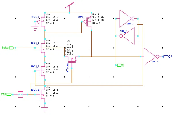
E. Proposed P-FF design
© 2014, IJCSMC All Rights Reserved 315
This design adopts a signal feed-through technique to improve the delay at the critical path. This design employs a static latch structure and a conditional discharge scheme to avoid superfluous switching activity at the internal node. A weak pull-up p-MOS transistor with gate connected to the ground is used in the first stage of the TSPC latch. This gives rise to a Pseudo-n-MOs logic style design, and the keeper circuit for the internal node X can be saved. In addition to the circuit simplicity, this approach also reduces the load capacitance at node X.A pass transistor MNx controlled by the pulse clock is included so that input data can drive node Q of the latch directly. The operation of the proposed design is as follows. When a clock pulse arrives, if no data transition occurs, i.e., the input data and node Q are at the same level, on current passes through the pass transistor, which keeps the input stage of the FF from any driving effort. At the same time, the input data and the output feedback assume complementary signal levels and the pull-down path of node X is off. Therefore no signal switching occurs in any internal nodes, on the other hand, if “0” to”1” data transition occurs, node X is discharged to turn on transistor MP2, which then pulls node Q high.
III. Simulation Results
The performance of proposed P-FF design is evaluated against existing design through pre layout simulations. With regard to the latch structures, every P-FF is design is individually optimized subject to the product of power and D-to-Q delay.
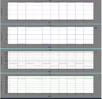
© 2014, IJCSMC All Rights Reserved 316 Fig 7: waveform of conditional discharge Flip Flop
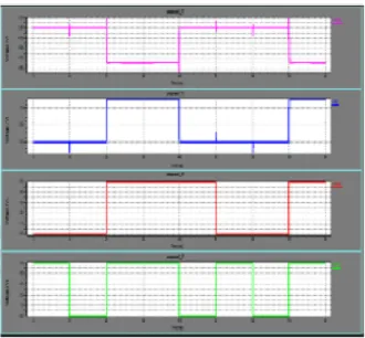
© 2014, IJCSMC All Rights Reserved 317 Fig 9: waveform of conditional pulse enhancement scheme
© 2014, IJCSMC All Rights Reserved 318 Table of Comparison:
IV. Conclusion
In this brief, we presented a novel P-FF design by employing a modified TSPC structure incorporating a mixed design style consisting of a pass transistor and a pseudo-n-MOS logic. The key idea was to provide a signal feed through from input source to the internal node of the latch, which would facilitate extra driving to shorten the transition time and enhance both power and speed performance.
References
[1] H. Kawaguchi and T. Sakurai, “A reduced clock-swing flip-flop (RCSFF) for 63% power reduction,” IEEE J.
Solid-State Circuits, vol. 33, no. 5, pp. 807–811, May 1998.
[2] K. Chen, “A 77% energy saving and J. Rabaey, flip-flops for high-performance microprocessors,” in Proc.
ISPLED, 2001, pp. 207–212.
[3] S. D. Naffziger, G. Colon-Bonet, T. Fischer, R. Riedlinger, T. J. Sullivan, and T. Grutkowski, “The implementation of the Itanium 2 microprocessor,” IEEE J. Solid-State Circuits, vol. 37, no. 11, pp. 1448–1460, Nov. 2002.
[4] S. Sadrossadat, H. Mostafa, and M. Anis, “Statistical design framework of sub-micron flip-flop circuits considering die-to-die and within-die variations,” IEEE Trans. Semicond. Manuf., vol. 24, no. 2, pp. 69–79, Feb. 2011.
[5] M. Alioto, E. Consoli, and G. Palumbo, “General strategies to design nanometer flip flops in the energy-delay space,” vol. 57, no. 7, pp. 1583–1596, Jul. 2010.
[6] M. Alioto, E. Consoli, and G. Palumbo, “Flip-flop energy/performance versus Clock Slope and impact on the clock network design,” IEEETrans. Circuits Syst., vol. 57, no. 6, pp. 1273–1286, Jun. 2010.
[7] M. Alioto, E. Consoli, and G. Palumbo, “Analysis and comparison in the energy-delay-area domain of nanometer CMOS flip-flops: Part I-methodology and design strategies,” IEEE Trans. Very Large Scale Integr. (VLSI) Syst., vol. 19, no. 5, pp. 725–736, May 2011.
[8] M. Alioto, E. Consoli and G. Palumbo, “Analysis and comparison in the energy-delay-area domain of nanometer CMOS flip-flops: Part II -results and figures of merit,” IEEE Trans. Very Large Scale Integr. (VLSI)Syst., vol. 19, no. 5, pp. 737–750, May 2011.
[9] B. Kong, S. Kim, and Y. Jun, “Conditional-capture flip-flop for statistical power reduction,” IEEE J. Solid-State Circuits, vol. 36, no. 8, pp. 1263–1271, Aug. 2001.
[10] N. Nedovic, M. Aleksic, and V. G. Oklobdzija, “Conditional precharge techniques for power-efficient dual-edge clocking,” in Proc. Int. Symp.Low-Power Electron. Design, Aug. 2002, pp. 56–59.
FF designs Ep-DCO CDFF
Ep-SFF
Conditional pulse
enhancement scheme
Proposed
Technique
Number of
transistors
28 30 14 19 12
Delay(ps) 118.9 129.5 145 107.24 182.4
Average power(µW) 34.41 34.08 71 31.11 30.09
© 2014, IJCSMC All Rights Reserved 319
[11] P. Zhao, T. Darwish, and M. Bayoumi, “High-performance and low power conditional discharge flip-flop,” IEEE Trans. Very Large ScaleIntegr. (VLSI) Syst., vol. 12, no. 5, pp. 477–484, May 2004.
[12] M.-W. Phyu, W.-L. Goh, and K.-S. Yeo, “A low-power static dual Edge triggered flip-flop using an output-controlled discharge configuration,” in Proc. IEEE Int. Symp. Circuits Syst., May 2005, pp. 2429–2432.