Effect of Coupled Inductor in Boost Converter
Sruthi P K1, Pranav M S2, Dhanya Rajan3
PG Student [Power Electronics], Dept. of EEE, Vidya Academy of Science and Technology, Thrissur, Kerala, India 1
PG Student [Power Electronics], Dept. of EEE, Vidya Academy of Science and Technology, Thrissur, Kerala, India2
PG Student [Power Electronics], Dept. of EEE, Vidya Academy of Science and Technology, Thrissur, Kerala, India3
ABSTRACT:This paper does the comparative analysis of effect of coupled inductor in soft switched boost converters
using SIMULINK. The comparison of the converter with or without coupled inductor have been done to identify which one is highly efficient in terms of performance, voltage stress, complexity etc. Simulation of the two topologies under the same condition are included in this paper. This paper should act as a reference for future work in the field of soft switched boost converter for high power application.
KEYWORDS:Boost converter, Coupled inductor, Soft switched
I.INTRODUCTION
There is an increasing demand for boost converters with power conditioning due to high and sudden variations in load such as DC drives. When switched at high frequency to obtain dynamic & steady state specifications, the losses increases in the converter. Turn on at zero current and turn off at zero voltage is one of the possible solution to reduce the switching losses. In order to achieve improved performance snubber circuits are introduced with boost converter.
At turn on instant a series inductor named as snubber inductor is included to limit the rate of rise of current through the switch. At turn off condition a shunt capacitor named as snubber capacitor is included to limit the rate of rise of voltage across the switch. At the time of snubbing energy is stored in the electric/magnetic field of these components. In order to ensure repetitive snubbing action, stored energy must be removed after every switching transition. The easy way is to discharge the stored energy into a resistor, which leads to dissipative snubber.
For high power application large snubber is required, which leads to huge amount of stored energy in the snubber element & simultaneously leads to more energy loss in snubber. Nowadays all electrical systems are focused towards high efficiency, in order to increase the performance, the use of energy recovery or non-dissipative snubber is introduced. This snubber have the capacity to recover a part of the stored energy by feeding it back to the supply or load. In this paper, the effect of dissipative and non-dissipative snubber is analysed at the same conditions. Performance evaluations are also presented with the help of MATLAB/SIMULINK
II. LITERATURE SURVEY
ISSN (Print) : 2320 – 3765 ISSN (Online): 2278 – 8875
I
nternational
J
ournal of
A
dvanced
R
esearch in
E
lectrical,
E
lectronics and
I
nstrumentation
E
ngineering
(An ISO 3297: 2007 Certified Organization)
Vol. 4, Issue 3, March 2015
III.STUDY OF DIFFERENT TOPOLOGIES
The 2 different topologies that are analysed in this paper are 1) Boost converter without coupled inductor
2) Boost converter with coupled inductor
1)Boost Converter without Coupled Inductor
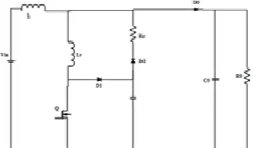
The proposed converter shown in Fig.1 is a simple boost topology with a snubber consisting of a resonant inductor (Lr), resonant capacitor (Cr), a reset resistor (Rr) and 2 diodes (D1 & D2). The boost inductor is denoted as L, Q is the switch, D0 is the output diode, C0 is the output capacitor, and R0 is the load.
Fig. 1Boost converter without coupling inductor
Operation:
This circuit is analyzed based on the conduction intervals of switches in different modes of operation. There are 8 modes of operation in this circuit.
Mode 1: The switch Q is off.
Mode 2: The switch Q is turned on under ZCS, D1 is reverse biased. At the end of this mode D0 is turned off and D2 is forward biased.
Mode 3: Resonance occurs between Lr and Cr. Complete discharging of Cr occurs at the end of this mode.
Mode 4: Diodes D1 and D2 are forward biased. In this mode energy stored in Lr is dissipated in Rr. Recovery of snubber occur during this mode.
Mode 5: Power from the source is transferred to the boost inductor Lr.
Mode 6: The switch Q is turned off. D1 is forward biased. At the end of this mode Cr is charged towards the output voltageV0.
Mode 7: Similar to mode 4. Rr resets Lr.
Mode 8: In this mode, D is forward biased and the power is transferred from the boost inductor to the load.
2)Boost Converter with Coupled Inductor
Fig. 2Boost converter with coupling inductor
Operation:
This circuit is analyzed based on the conduction intervals of switches in different modes of operation. There are seven modes of operation in this circuit.
Mode 1 (before t0): The switch Q is off, D1 and D2 are blocked, converter is in freewheeling stage.
Mode 2 (t0 - t1): At t0, Q is on under ZCS. D1 and D2 are still blocked.
Mode 3 (t1 - t2):At t1, VC1 = V0, D0 is off under ZVS. D1 and D2 are still blocked. C1 and L2 begin to resonate.
Mode 4 (t2 - t3):As VL3 = VC2 at t2 i.e., VC2= Vb = N1 VC1(t2) then D2 forward biased and stored energy in C2 is transferred to L3.
Mode 5 (t3 - t4): At t3, VC1 = VC2 = 0 then D1 conducts. The stored energy in C1 and C2 is transferred to L2 and L3 completely.
Mode 6 (t4 - t5): At t4, switch Q turns off under ZVS. Double resonance occur between L2, L3 and C1, C2$. The stored energy in L2, L3 transferred to C1, C2.
Mode 7 (t5-t6):At t5, VC1 = V0, then D0 conducts
III.SIMULATION RESULTS AND DISCUSSIONS
The 2 topologies are simulated in MATLAB/SIMULINK, with the following common parameters
Table -1: Simulation Parameters
Parameter Values
Supply voltage 55 V
Duty ratio (D) 0.5
Switching frequency (fsw) 30 kHz Coupling inductor (Lr1) 20 µH
Load (R0) 25 Ω
ISSN (Print) : 2320 – 3765 ISSN (Online): 2278 – 8875
I
nternational
J
ournal of
A
dvanced
R
esearch in
E
lectrical,
E
lectronics and
I
nstrumentation
E
ngineering
(An ISO 3297: 2007 Certified Organization)
Vol. 4, Issue 3, March 2015
Fig. 3Simulation diagram of boost converter without coupled inductor
The output voltage of the waveform is greater than 100 V. So that gain of the converter is approximately equal to 2. The simulation diagram of the proposed converter is shown in fig 3, output waveform is shown in Fig.4 and the switching waveforms are in Fig.5.
Fig .4 Output waveform of boost converter without coupled inductor
The switch stress is greater than 143 V and peak switch current is larger than 14A.From the switching waveforms it is very clear that the switch is turned on at ZCS and turned off at ZVS, hence switching losses are reduced.
Fig .6 Simulation diagram of boost converter with coupled inductor
The output voltage of the waveform is lower than 100 V. So that gain of the converter is lesser than that of converter [1]. The simulation diagram of the proposed converter is shown in fig 6, output waveform is shown in Fig.7 and the switching waveforms are in Fig.8.
Fig .7 Output waveform of boost converter with coupled inductor
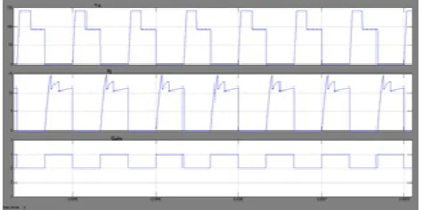
The switch stress is lesser than 143 V and peak switch current is larger than 14A.From the switching waveforms it is very clear that the switch is turned on at ZCS and turned off at ZVS, hence switching losses are reduced.The efficiency of the converter is found to be greater than 90%.
Fig .8 Waveforms of VQ, IQ and gate of boost converter with coupled inductor
ISSN (Print) : 2320 – 3765 ISSN (Online): 2278 – 8875
I
nternational
J
ournal of
A
dvanced
R
esearch in
E
lectrical,
E
lectronics and
I
nstrumentation
E
ngineering
(An ISO 3297: 2007 Certified Organization)
Vol. 4, Issue 3, March 2015
Table -2:Comparison between the 2 Topologies Based on the Various Parameters
Parameters
Converter of [1]
Converter of [2]
Output voltage (V) 102.57 93.3
Voltage gain 1.864 1.6963
Output power (W) 420.8 348.2
Efficiency (%) 85.40 93.08
Voltage stress on the switch (V) 143.757 142 Peak switch current (A) 14.75 14.615 Voltage stress on output diode (V) 0.812 0.823
Number of extra components 5 6
Inference:
A comparison of 2 different soft switched topologies are shown in Table I. The simulation is performed by MATLAB/SIMULINK using the same parameters. The results shows that converter of [2] has higher efficiency, less voltage stress, reduced peak switch current. The number of components used in converter of [2] is less compared to converter of [1] but the performance is poor in terms of efficiency.
VI.CONCLUSION
This paper presents analysis of soft-switched boost converter topologies with the effect of coupled inductor. The converter of [1] act analogous to conventional hard switched converter & soft-switched converter with auxiliary switches. In addition to efficiency a wide soft switching range is provided by non-dissipative snubber but the system become complex. The comparison table should serve as a reference in selecting the right converter topology for various applications related to renewable energy. The simulation results of 2 topologies for an input voltage of 55V and load of 25Ω are presented.
REFERENCES
[1] J.M.Kwon,W.Y.Choi and B. H. Kwon, “Cost -effective boost converter with reverse recovery reduction and power factor correction, "IEEE Trans. Industrial Electron., vol. 55, no. 1, pp. 471 -- 473, Jan.2008.
[2] D. Garabandic, M. Kuzmanovic, and W. Dunford," A low-loss 2D-C-L-R resonant snubber for single-switch soft-switching boost DC/DC converters,"in Proc. IEEE Canadian Conf. Electr. Comput. Eng., 1998, vol. 2, pp. 858–861.
[3] Q. Zhao, F. Tao, F. C. Lee, P. Xu, and J. Wei, " Novel family of pwm soft-single-switched dc-dc converters with coupled inductors " IEEE Trans. Industrial Electron., vol. 56,no. 6, pp. 2108 -- 2114, Jun. 2009.
[4] T.Zhan, Y.Zhang,J.Nie and Y. Zhang, "A novel soft-switching boost converter with magnetically coupled resonant snubber, "IEEE Trans. Power Electron., vol. 29, no. 11, pp. 5680 –- 5687, Nov. 2014.
[5] M. M. Jovanovic and Y. Jang, "A novel active snubber for high-power boost converters, "IEEE Trans. Power Electron., vol. 15, no. 2, pp. 278 – 284, Mar. 2000.
[6] H. Bodur and A. F. Bakan, "A new ZVT – ZCT – PWM DC – DC converter, "IEEE Trans. Power Electron., vol. 19, no. 3, pp. 676 - 684, May 2004..
[7] Q. Zhao, F. Tao, F. C. Lee, P. Xu, and J. Wei, "A simple and effective method to alleviate the rectifier reverse-recovery problem in continuous current-mode boost converters, IEEE Trans. Power Electron., vol. 16,no. 5, pp. 649 -- 658, Sep. 2001.
[8] S.-R. Park, S.-H. Park, C.-Y. Won, and Y.-C. Jung, "Low loss soft switching boost converter," Proc. 13th Power Electron. Motion Control Conf., 2008, pp. 181 –- 186.
[9] N Jain, P Jain, and G Joos, “Designing a zero voltage transition boost converter for power factor corrected modular telecom rectifiers,"Proc.
23th Int. Telecommun. Energy Conf., 2001, pp. 139 –- 145.
[10] M. Kobayashi and N. Kasa," Analysis of a coupled inductor for zero current transition boost converters," Proc. Int. Conf. Power Electron. DriveSyst., pp. 7 –- 11, 2009.
[11] S. Y. R. Hui, K. W. E. Cheng, and S. R. N. Prakash, "A fully soft-switched extended-period quasi-resonant power-factor-correction circuit," IEEE Trans. Power Electron., vol. 12, no. 5, pp. 922 –- 930, Sep. 1997.
[12] S. S. Saha and B. Majumdar," New fully soft-switched boost-converter with reduced conduction losses," Proc. Int. Conf. Power Electron. Drives Syst., 2005, pp. 107 -– 112.
[13] P. Shuai, Y. R. De Novaes, F. Canales, and I. Barbi, “A non-insulated resonant boost converter,"Proc. IEEE 25th Annu. Appl. Power Electron.Conf. Expo, 2010, pp. 550 –- 556.