International Journal of Research (IJR)
e-ISSN: 2348-6848, p- ISSN: 2348-795X Volume 2, Issue 06, June 2015Available at http://internationaljournalofresearch.org
Realization of Data Encoding Schemes in Network on Chip
Using Verilog HDI
Boggarapu Kantha Rao
1; K.Radha
2& Penti Supraja
31H.O.D ASSOCIATE PROFESSOR Dept of ECE,Medha Institute of science and Technology for
women,Khammam, Telangana
2ASSOCIATE PROFESSOR Dept of ECE,Medha Institute of science and Technology for women,
Khammam, Telangana
3STUDENT Dept of ECE,Medha Institute of science and Technology for women,Khammam,
Telangana
Abstract:
Power has become a paramount design criterion in modern system designs, especially in portable battery-driven applications. A paramount portion of total power dissipation is due to the transitions on the off-chip address buses. This is because of the astronomically immense switching capacitances associated with these bus lines. There are many encoding schemes in the literature that achieve an immensely colossal reduction in transition activity on the ordinant dictation address bus. However, on data and multiplexed address buses, none of the subsisting schemes consistently achieve consequential reduction in transition activity. Additionally, many of the subsisting techniques integrate redundancy in space and/or time. In this paper, novel
encoding schemes are proposed that
significantly reduce transitions on these buses without integrating redundancy in space or time. Additionally, for applications with tight delay constraints, configurations with minimal delay overhead while still achieving paramount reduction in transition activity are proposed. Results show that, for sundry benchmark programs, these techniques achieve reduction of up to 54% in transition activity on a data address bus. On a multiplexed address bus, there is a reduction of up to 61% utilizing our techniques. The proposed schemes are then compared with the subsisting schemes. It is optically discerned that on an average, the reductions achieved by our techniques are twice those obtained utilizing the current scheme on a data address bus and 55% more than those for multiplexed address bus.
Keywords: Binary to gray conversion; Data encoding; Interconnection on chip; Low power; Network-on-chip (NOC); Power analysis; Gray to binary conversion.
Introduction
As VLSI technologies perpetuate to scale, wire densities increases to fortify ever-minuscule transistor geometries and casuses on-chip wires to present incrementing latency and energy quandary. In particular, the high latency of cross-chip communication can still limit total performance by incrementing the delay between on-chip unit. Such scalable bandwidth requisite can be satiated by utilizing on-chip
packet-switched micro-network of
interconnects, generally kenned as Network-on-Chip (NoC) architecture. The rudimental conception emanated from the traditional sizably voluminous-scale multi-processors and distributed computing networks. The scalable and modular nature of NoC and their fortification for efficient onchip communication
lead to the NoC-predicated system
implementations. In order to meet typical SoCs or multicore multiprocessing and rudimentary module of network interconnection like switching logic, routing algorithm and the packet definition should be light-weighted to result in facilely implemental solutions.
International Journal of Research (IJR)
e-ISSN: 2348-6848, p- ISSN: 2348-795X Volume 2, Issue 06, June 2015Available at http://internationaljournalofresearch.org
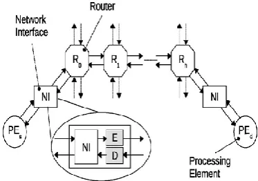
Chip (NoC) architecture. Fundamental concept of such kind of interconnections emanates from the modern computer network evolution as mentioned afore. By applying network-like communication which inserts some routers in-between each communication object, the required wiring can be minimized. Therefore, the switch-predicated interconnection mechanism provides a plethora of scalability and liberation from the circumscription of involute wiring. Supersession of SoC busses by NoCs will follow the same path of data communications when the economics prove that the NoC either reduces SoC manufacturing cost, SoC time to market, SoC time to volume, and SoC design risk or increases SoC performance.
According to the NoC approach has a clear advantage over traditional busses and most eminently system throughput. And hierarchies of crossbars or multilayered busses have characteristics somewhere in between traditional busses and NoC, however they still fall far short of the NoC with veneration to performance and involution.The prosperity of the NoC design depends on the research of the interfaces between processing elements of NoC and interconnection fabric. The interconnection of a SoC established procedures has some impuissant points in those venerations of slow bus replication time, energy circumscription, scalability quandary and bandwidth inhibition. Bus interconnection composed of an
astronomically immense number of
components in a network interface can cause slow interface time though the influence of sharing the bus. In integration the interconnection has a defect that power consumption is high on the score of connecting all objects in the communication. Moreover it is infeasible to increment the number of connection of the elements illimitably by reason of the circumscription of bandwidth in a bus.
As a consequence, the performance of the NoC design relies greatly on the interconnection paradigm .Though the network technology in computer network is already well developed, it
is virtually infeasible to apply to a chip-level intercommunication environment without any modification or reduction. For that reason, many researchers are endeavoring to develop felicitous network architectures for on-chip communication. To be eligible for NoC architecture, the rudimentary
functionality should be simple and light-weighted because the implemented component of NoC architecture should be minute enough to be a fundamental component constructing a SoC. In order to be low powered one has to consider many parameters such as clock rate, operating voltages, power management.
Fig 1: Fundamental concept of NOC.
International Journal of Research (IJR)
e-ISSN: 2348-6848, p- ISSN: 2348-795X Volume 2, Issue 06, June 2015Available at http://internationaljournalofresearch.org
interleaved in the same link is not valid anymore. At any rate, it does not denote that the proposed scheme cannot be applied in VC predicated implementations but, instead, that the potential power savings are reduced.
1.
Related Work
In the next several years, the availability of the chips with 1000 cores is premised [6]. In these chips, a consequential fraction of the total system power budget is dissipated by interconnection network. Therefore, the design of power efficient interconnection networks has been the focus of many works published in the literature dealing with NoC architecture. These works concentrate on different components of the interconnection networks such as routers, NI, and links. Since the focus of this paper is on reducing the puissance dissipation by the links, in this section, briefly review some of the works in the area of link power reduction. These include the techniques that make utilization of shielding [7], [8], incrementing line-to-line spacing [9], [10], repeater insertion [11]. They all increase the chip area. The data encoding scheme is another method that was employed to reducing the link power dissipation. The data encoding techniques may be relegated into two types. In the first type, encoding techniques concentrate on lowering the potency due to self-switching activity of individual bus lines while ignoring the puissance dissipation owing to their coupling switching activity. In this type, bus invert (BI) [12] and INC-XOR [13] have been proposed for the case that arbitrary data patterns are transmitted through these lines. On the other hand, gray code [14], T0 [15], working-zone encoding [16], and T0-XOR [17] were suggested for the case of correlated data patterns. Application specific approaches have additionally been proposed [18]–[22].This category of encoding is not opportune to applied in the deep sub micron meter technology nodes where the coupling capacitance constitutes a major part of the total interconnect capacitance. This causes the puissance consumption due to the coupling switching activity to become an immensely
International Journal of Research (IJR)
e-ISSN: 2348-6848, p- ISSN: 2348-795X Volume 2, Issue 06, June 2015Available at http://internationaljournalofresearch.org
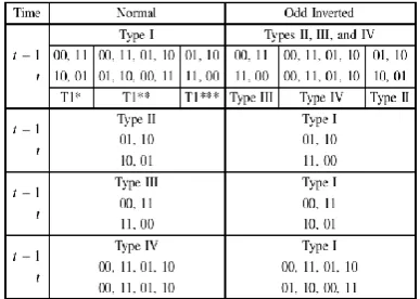
Table 1: Effect of Odd Inversion on Change of Transition Types.
2.
Implementation
3.1 Proposed Encoding Schemes:
In this section, present the proposed encoding scheme whose goal is to reduce power dissipation by minimizing the coupling transition activity on the links of the interconnection network. Let us first describe the puissance model that contains the different components of puissance dissipation of a link.. One can relegate four types of coupling transitions. A Type I transition occurs when one of the lines switches when the other remains unchanged. In a Type II transition, one line switches from low to high, other makes transition from high to low .A Type III transition corresponds to the case where both lines switch simultaneously. Determinately, in a Type IV transition both lines do not transmute. The efficacious switched capacitance varies from type to indite and hence, the coupling transition activity, is a weighted sum of variants of coupling transition contributions .Here, we calculate the occurrence probability for variants of transitions. Consider that flit ( t − 1) and flit ( t ) refer to the antecedent flit which was transferred through the link and the flit is about to pass through the link, respectively.We consider only two adjacent bits of the physical channel.Sixteen different coalescences of these four bits could occur (Table I). Note that the first bit is the value of the generic i th line of the link, whereas the second bit represents the value of its ( i + 1)th line. The number of transitions for Types I, II, III, and IV are 8, 2, 2,
and 4, respectively. For an arbitrary set of data, each of these sixteen transitions has the same probability. Therefore, the occurrence probability for Types I, II, III, and IV are 1/2, 1/8, 1/8, and 1/4, respectively. In the rest of this section, we present three data encoding schemes designed for reducing the dynamic power dissipation of the network links along with a possible hardware implementation of the decoder.
3.1(a) SCHEME I:
In Scheme I, we fixate on reducing Type I transitions while in Scheme II, both Types I and II transitions are taken into account for deciding between half and full invert, depending the amount of switching reduction. Determinately, in Scheme III, we consider the fact that Type I transitions show different comportments in the case of eccentric and even invert and make the inversion which leads to the higher power preserving.
Fig 2: Circuit diagram of encoder architecture of scheme I.
International Journal of Research (IJR)
e-ISSN: 2348-6848, p- ISSN: 2348-795X Volume 2, Issue 06, June 2015Available at http://internationaljournalofresearch.org
In scheme I, we fixate on reducing the numbers of Type I transitions ( by converting them to Types III and IV transitions) and Type II transitions (by converting them to Type I transition). The scheme compare the current data with the antecedent data one to decide whether aberrant inversion or no inversion of the current data can lead to the link power reduction. Table I reports, for each transition, the relationship between the coupling transition activities of the flit when transmitted and when its bits are eccentric inverted. Data are organized as follows. The first bit is the value of the generic i th line of thelink, whereas the second bit represent the value of its ( i + 1)th line. For each partition, the first line represents the values at time t − 1(t). As Table I shows, if the flit is aberrant inverted, Types II, III, and IV transitions convert to Type I transitions. In the case of Type I transitions, the inversion leads to one of Types II, III, or Type IV transitions. In particular, the transitions betokened as T∗1, T∗∗1,andT∗∗∗1 in the table convert to Types II, III, and IV transitions, respectively.
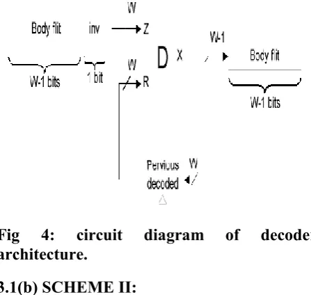
Fig 4: circuit diagram of decoder architecture.
3.1(b) SCHEME II:
In the proposed encoding scheme II, we make utilization of both aberrant (as discussed anteriorly) and full inversion. The full inversion operation converts Type II transitions to Type IV transitions. The scheme compares the current data with the precedent one to decide whether the aberrant, plenary, or no inversion
of the current data can give elevate to the link power reduction.
Fig 4: Encoder architecture scheme II.
Fig 5: Internal view of the decoder block scheme II.
International Journal of Research (IJR)
e-ISSN: 2348-6848, p- ISSN: 2348-795X Volume 2, Issue 06, June 2015Available at http://internationaljournalofresearch.org
the overhead of the decoder hardware could be substantially reduced.
This module determines if aberrant, even, plenary, or no invert action corresponding to the outputs “10,”“01,” “11,” or “00,” respectively, should be performed. The outputs “01,” “11,” and “10” show that whether respectively, are gratified. In this paper, Module C was designed predicated on the conditions given .Similar to the procedure used to design the decoder for scheme II, the decoder for scheme III may be designed .This article has been accepted for inclusion in a future issue of this journal. Content is final as presented, with the exception.
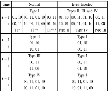
Table 2: Effect of Even Inversion on Change of Transition Types.
3.1(c) SCHEME III:
In the proposed encoding Scheme III, we integrate even inversion to Scheme II. The reason is that aberrant inversion converts some of Type I ( T∗∗∗1) transitions to Type II transitions. As can be observed from Table II, if the flit is even inverted, the transitions designated as T∗∗1/ T∗∗∗1 in the table are converted to Type IV/Type III transitions. Therefore, the even inversion may reduce the link power dissipation as well. The scheme compares the current data with the anterior one to decide whether eccentric, even, plenary, or no inversion of the current data can give elevate to the link power reduction.
Fig 6: Encoder architecture scheme III.
3. Experimental Results
Dynamic Power Dissipation for Encoder:
ENC O DER (TRA DITI O NAL)
ENCODE R(
PROPOSE D
)
SCHEME –I
ENCOD E
R(PROP O SED) SCHEM E –II
ENCODE R(
PROPOSE D
)
SCHEME –
III 19.45
mw
19.43mw 7.76mw 7.87mw
International Journal of Research (IJR)
e-ISSN: 2348-6848, p- ISSN: 2348-795X Volume 2, Issue 06, June 2015Available at http://internationaljournalofresearch.org
DECO DE R (TRAD IT IONAL )
DECODE R(P ROPOSE D)
SCHEME –I
DECODER (PR
OPOSED) SCHEME -II
DECO DE R(PRO PO SED) SCHE ME –III 19.35m
w
16.19mw 10.37mw 7.66mw
4. Conclusion
In this paper, a set of incipient data encoding schemes aimed at reducing the puissance dissipated by the links of an NoC. As compared to the antecedent encoding schemes the rationale abaft the proposed schemes is to minimize not only the switching activity, but additionally the coupling switching activity which is mainly responsible for link power dissipation. By utilizing the proposed encoding schemes in NoC architecture their application does not require any modification neither in the routers nor in the links. As per the performance evaluation results, the proposed system has lower dynamic power dissipation than classical one.
5. References
[1] International Technology Roadmap for
Semiconductors.(2011) [Online].Available:
http://www.itrs.net
[2] M. S. Rahaman and M. H. Chowdhury, “Crosstalk avoidance and errorcorrection coding for coupled RLC interconnects,” in Proc. IEEE Int. Symp. Circuits Syst., May 2009, pp. 141–144.
[3] W. Wolf, A. A. Jerraya, and G. Martin, “Multiprocessor system-on-chip MPSoC technology,” IEEE Trans. Comput.-Aided Design Integr. Circuits Syst., vol. 27, no. 10, pp. 1701–1713, Oct. 2008.
[4] L. Benini and G. De Micheli, “Networks on chips: A new SoC paradigm,” Computer, vol. 35, no. 1, pp. 70–78, Jan. 2002.
[5] S. E. Lee and N. Bagherzadeh, “A variable frequency link for a poweraware network-on-chip (NoC),” Integr. VLSI J. , vol. 42, no. 4,pp. 479– 485, Sep. 2009.
[6]D.Yeh,L.S.Peh,S.Borkar,J.Darringer,A.Agar
wal,andW.M.Hwu,“Thousandcore chips
roundtable,” IEEE Design Test Comput., vol. 25,no. 3, pp. 272–278, May–Jun. 2008.
[7] A. Vittal and M. Marek-Sadowska, “Crosstalk reduction for VLSI,”IEEE Trans. Comput.-Aided Design Integr. Circuits Syst. , vol. 16, no. 3,pp. 290–298, Mar. 1997.
[8] M. Ghoneima, Y. I. Ismail, M. M. Khellah, J. W. Tschanz,and V. De,“Formal derivation of optimal active shielding for low-power onchip buses,” IEEE Trans. Comput.-Aided Design Integr. Circuits Syst. , vol. 25,no. 5, pp. 821– 836, May 2006.
[9] L. Macchiarulo, E. Macii, and M. Poncino, “Wire placement for crosstalk energy minimization in address buses,” in Proc. Design Autom.Test Eur. Conf. Exhibit. , Mar. 2002, pp. 158–162.
International Journal of Research (IJR)
e-ISSN: 2348-6848, p- ISSN: 2348-795X Volume 2, Issue 06, June 2015Available at http://internationaljournalofresearch.org
[11] K. Banerjee and A. Mehrotra, “A power-optimal repeater insertion methodology for global inter connects in nanometer designs,” IEEE Trans. Electron Devices , vol. 49, no. 11, pp. 2001–2007, Nov. 2002.
[12] M. R. Stan and W. P. Burleson, “Bus-invert coding for low-power I/O,” IEEE Trans. Very Large Scale Integr. (VLSI) Syst. , vol. 3, no. 1,pp. 49– 58, Mar. 1995.
[13] S. Ramprasad, N. R. Shanbhag, and I. N. Hajj, “A coding frameworkfor low-power address and data busses,” IEEE Trans. Very Large Scale Integr. (VLSI) Syst. , vol. 7, no. 2, pp. 212–221, Jun. 1999.
[14] C. L. Su, C. Y. Tsui, and A. M. Despain, “Saving power in the control path of embedded processors,” IEEE Design Test Comput. , vol. 11, no. 4,pp. 24–31, Oct.–Dec. 1994.
[15] L. Benini, G. De Micheli, E. Macii, D. Sciuto, and C. Silvano, “Asymptotic zero-transition activity encoding for address busses in low-power microprocessor-based systems,” inProc. 7th Great Lakes Symp. VLSI,Mar. 1997, pp. 77–82.
[16] E. Musoll, T. Lang, and J. Cortade lla, “Working-zone encoding for reducing the energy in microprocessor address buses,” IEEE Trans. Very Large Scale Integr. (VLSI) Syst. , vol. 6, no. 4, pp. 568–572, Dec. 1998.
[17] W. Fornaciari, M. Polentarutti, D. Sciuto, and C. Silvano,“Power optimization of system-level address buses based on software profiling,” in Proc. 8th Int. Workshop Hardw. Softw. Codesign, May 2000,pp. 29– 33.
[18] L. Benini, G. De Micheli, E. Mac ii, M. Poncino, and S.Quer, “Power optimization of core-based systems by address bus encoding,” IEEE Trans. Very Large Scale Integr. (VLSI) Syst. , vol. 6, no. 4, pp. 554– 562, Dec. 1998.
[19] L. Benini, A. Macii, M. Poncino, and R. Scarsi,“Architectures and synthesis algorithms for power-efficient bus interfaces,” IEEE Trans.Comput.-Aided Design Integr.Circuits Syst., vol. 19, no. 9, pp. 969– 980,Sep. 2000.
[20] G. Ascia, V. Catania, M. Palesi , and A. Parlato,“Switching activity reduction in embedded systems: Agenetic bus encoding approach,”IEEE Proc. Comput. Digit. Tech. , vol. 152, no. 6, pp. 756–764, Nov. 2005.
[21] R. Siegmund, C. Kretzschmar, and D. Muller, “Adaptive Partial Businvert encoding for power efficient data transfer over wide system buses,” in Proc. 13th Symp. Integr. Circuits Syst. Design, Sep. 2000,pp. 371–376.
[22] S. Youngsoo, C. Soo-Ik, and C. Kiyoung, “Partial bus- invert coding for power optimization of application- specific systems,” IEEE Trans. Very Large Scale Integr. (VLSI) Syst. , vol. 9, no. 2, pp. 377–383, Apr. 2001.
[23] M. Palesi, G. Ascia, F. Fazzino, and V. Catania, “Data encoding schemes in networks on chip,” IEEE Trans. Comput.-Aided Design Integr. Circuits Syst. , vol. 30, no. 5, pp. 774– 786, May 2011.
[24] C. G. Lyuh and T. Kim, “Low-power bus encoding with crosstalk delay elimination,” IEE Proc. Comput. Digit.Tech. , vol. 153, no. 2,pp. 93– 100, Mar. 2006.