660
Design & Simulation of 2-bit Full Adder Using Different
CMOS Technology
Pranay Kumar Rahi1, Shashi Dewangan2, Nishant Yadav3
1
ME Scholar, 2Assistant Professor, 3MTech Scholor,
1
Department of Electronics & Communication Engineering
National Institute of Technical Teachers’ Training & Research,Chandigarh, UT, India
2
Department of Physics
Kamala Nehru College, Korba, Chhattisgarh, India
3
Department of Computer Science and Engineering, Indian Institute of Technology, Kharagpur, West Bengal, India
ABSTRACT
A fast and energy-efficient Full Adder plays important role in electronics industry especially digital signal processing (DSP), image processing and performing arithmetic operations in microprocessors. Full Adder is such an important element which contributes substantially to the total power consumption of the system. In this paper, proposed 2-bit Full Adder has been taken which is then analyzed and a comparative study of the silicon area and the power consumption has been done in the circuit using different channel lengths such as 90nm, 70nm and 50nm. The designed circuit has shown a remarkable reduction in the consumed power of 94.5% and a reduction of 75.03% in consumed area in 50nm foundry as compared to 90nm COMS technologies. The designed Full adder are compared in terms of power consumption and surface area product using DSCH and MICROWIND tools.
KEYWORDS: CMOS, VLSI, Full Adder, Power consumption, CMOS technology.
1.
INTRODUCTION
With the advance of VLSI technology, to either speed up the operation or reduce the power/energy consumption hardware implementation of many applications such as multimedia processing, digital communication can be possible. The essence of the approximately all digital computing lies in the full adder design [5]. Addition forms the basis for many processing operations, from
counting to multiplication to filtering. As a result, adder circuits are of great interest to digital system designers. Adders are important components in the applications like Digital Signal Processing (DSP) architectures. For signal processing, digital full-adder are the basic logic circuits which can find applications in digital computing and packet labels processing. Addition is the most basic arithmetic operation; and adder is the most fundamental arithmetic component of the processor. The rapid increase in the number of transistors on chips has enabled a dramatic increase in the performance of computing systems. Computations need to be performed using low- power, area-efficient circuits operating at greater speed [1].
2.
FULL ADDER CIRCUITS
The Full-Adder (FA) is used widely in systems with operations such as counter, addition, subtraction, multiplication and division etc. It is the basic core component of Arithmetic-Logic-Unit (ALU). Thus, the innovation and acceleration of FA means that the speed of the Central-Processor-Unit [3]. Adder is the most important operation in any digital logic design. High speed and accurate operation of any digital system is influenced by its performance of the adder design. Pseudo NMOS and Pass-transistor logic can reduce the number of transistors required to implement a given logic function but suffers with power dissipation. The XOR gate using CMOS inverter and pass transistor and the conventional full adder and full adder design using dual sleep approach. These circuits are considered as the basic circuits in this paper. The size of the transistor
is defined as a ratio of Width/Length (W/L). Ground bounce noise is estimated when the circuits are connected with a sleep transistor. Sub-threshold current is directly proportional to the Width/Length ratio of transistor [2].
Fig.1-bit Full Adder Circuits
The most commonly used adder with complementary pull-up pMOS and pull-down nMOS networks in digital circuits is conventional 28 transistor full adder. A complementary static CMOS full adder circuit consists of an NMOS pull down network connecting the ground to the output and a dual pMOS pull up network connecting the power to the output. This adder implements the following Boolean equations [5]:
CARRY = A.B + B.Cin + A.Cin ……. (1)
SUM = A.B.Cin + CARRY (A + B + Cin) …..(2)
(a) Gate-level logic (b) HA based design
(c) Combinational Adder
Fig.2 Full Adder Circuits
A basic full adder has three inputs and two outputs which are sum and carry. The logic circuit of this full adder can be implemented with the help of XOR gate, AND gates and OR gates. The logic for sum requires XOR gate while the logic for carry requires AND, OR gates. The basic logic diagram for full adder using its Boolean equations with basic gates can be represented as shown below [4].
Fig.3 Schematic diagram of Full Adder
Table-1 Truth Table of Full Adder
A B Cin S Cout
0 0 0 0 0
0 0 1 1 0
0 1 0 1 0
0 1 1 0 1
662
The layout design of the basic full adder is shown in fig.4 layout is the general concept that describes the geometrical representation of the circuits by the means of layers. Different logical layers is used by designers to generate the layout [4].
Fig.4 Layout diagram of Full Adder
3.
LAYOUT SIMULATION
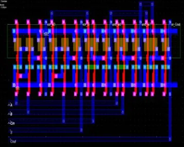
Performance analysis of full adder is presented in this section. Designs are simulated using DSCH and MICROWIND Tools at different technologies like 90nm, 70nm, 50nm. The layout design rule describes how the small features can be and how closely they can be packed in particular manufacturing process. Different logical layers are used by the designers to generate the layout. There are specific layers for metal, contacts or diffusion areas, polysilicon. In the layout design red color presents polysilicon, green color indicates n+ diffusion, light green color indicates p+ diffusion, light and dark blue color.
Fig.4 MICROWIND Layout design of Full Adder
4.
RESULTS
The proposed 2-bit Full Adder are compared based on the performance parameters like surface area and power dissipation. To achieve better performance, the circuits are designed using CMOS process by Microwind 3.1 in 50nm, 70nm and 90 nm technology. The proposed 2-bit Full Adder circuit shown in figure 3, uses two 2-bit X-OR, one 2-bit OR and two 2-bit AND logic gates.
Fig. 5 :Output of proposed multiplier using 50 nm CMOS Technology
Fig. 7: Output of proposed multiplier using 90 nm CMOS Technology
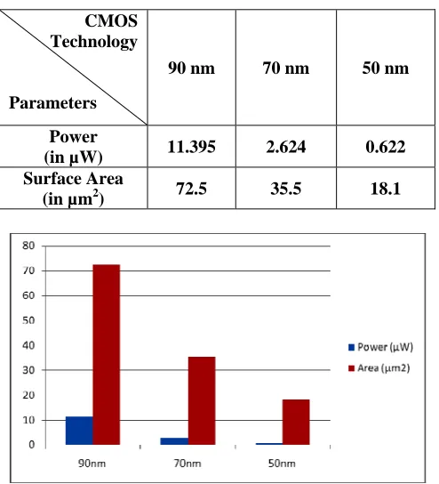
The comparative results for proposed 2-bit Full Adder for 50nm, 70nm and 90 nm CMOS design technology are given in Table-2.
Table 2. Power and surface area analysis of 2-bit Full adder in different CMOS technologies
CMOS Technology
Parameters
90 nm 70 nm 50 nm
Power
(in µW) 11.395 2.624 0.622
Surface Area
(in µm2) 72.5 35.5 18.1
Fig.8 Graphical Comparison of Power and Area
5.
CONCLUSION
proposed 2-bit Full Adder using the proposed logic in results reduction in the power and surface area. The power consumed by the circuit in 90nm, 70nm and 50nm CMOS technologies are 11.395µW, 2.624 µW and 0.622 µW respectively. The surface area consumed by the circuit in 90nm, 70nm and 50nm CMOS technologies are 72.5µm2, 35.5 µm2, and 18.1µm2 respectively.
REFERENCES
[1] Ranjeeta Verma, Rajesh Mehra, “CMOS Based Design Simulation of Adder /Subtractor Using Different Foundries”, International Journal of Science and Engineering (IJSE) ISSN: 2347-2200, Volume-2, Number-1, pp. 28-34, 2013. [2] T Krishna Moorthy, M.Balaji, G.Naresh, “Low Power
Dissipation of 4 bit Parallel adder/subtractor using Dual sleep and ground bounce technique in 120nm and 90nm Technology”, International Journal of VLSI and Embedded Systems (IJVES) ISSN: 2249-6556, Volume-4, Article-10162, pp. 610-614, October 2013
[3] TranBichThuan Pham, Yi Wang, Renfa Li, “Designing one-bit Full-Adder/Subtractor based on Multiplexer and LUT’s architecture on FPGA” International Journal of Digital Content Technology and its Applications(JDCTA), Volume-7, Number-8, pp. 455-464, April 2013
[4] Vandana Choudhary, Rajesh Mehra, “2- Bit Comparator Using Different Logic Style of Full Adder”, International Journal of Soft Computing and Engineering (IJSCE) ISSN: 2231-2307, Volume-3, Issue-2, pp. 277-279,May 2013
[5] Ruchika Sharma, Rajesh Mehra, “Design And Performance Analysis of CMOS Full Adder With 14 Transistor”, International Journal of Computer Technology and
Applications (IJCTA), ISSN:2229-6093, Volume 5, pp.
1461-1465, July-August 2014.
[6] Arun Gangwar, Rajesh Mehra, “CMOS Design And Low Power Full Adder Using .12 Micron Technology”, International Journal of Research In Computer Applications
And Robotics, ISSN 2320-7345,Volume-1, Issue-2, pp. 1-6
March-April: 2013.
AUTHORS
Pranay Kumar Rahi received the Bachelors of Technology degree in Electronics and Telecommunication Engi- neering from Government Engineering College, Guru Gasidas University, Bilaspur, Chhattisgarh, India in 2004, and pursuing Masters of Engineering in Electronics and
664
College, Korba, Chhattisgarh, India in 2007 and the Masters of Science degree in Physics from Government Science College, Guru Ghasidas University, Bilaspur, India in 2010. She is an Assistant Professor in the Department of Physics, Kamala Nehru College, Korba, India.
Nishant Yadav received the Bachelors of Technology degree in Computer Science and Engineering from Government Engineering College, Guru Ghasidas University, Bilaspur,
India in 2004, and pursuing Masters