Comparative Analysis of Area-Efficient Low
Power 1-Bit Full Adders at 65-Nm Technology
G.T.Bharathy
1, S. Philomina
*2Assistant Professor, Dept. of ECE, Jerusalem College of Engineering, 1
Assistant Professor, Dept. of ECE, Bharath University, Chennai, Tamil Nadu, India2
*
Corresponding Author
ABSTRACT: In this Paper we present Low power and Area-efficient 1-Bit Full adder designs featuring Conventional CMOS, CPL, PTL and XNOR-XNOR CMOS design styles. Area-efficiency is one of the most required features of the modern electronic System designed for high performance and Portable applications. We carried out a Comparison between these designs reported as in terms of Speed, Power dissipation and Area. The proposed full adders are area- efficient and outperform several standard Full adders without trading of driving capabilities and reliabilities. The new Full adders successfully operate at low voltage with excellent Signal integrity and Driving Capability. XNOR-XNOR based design full adder is more reliable in terms of Area, Power dissipation and Speed than other two proposed designs. All the Schematics and Layouts of these full adders were designed with a 65-nm CMOS technology using Micro wind 3.1.
KEYWORDS: Full Adder, Centralized, CPL, PTL, XNOR, Low Power
I. INTRODUCTION
CMOS VLSI circuits have been evolving into low voltage and low power regimes. In recent years VLSI design space has been focusing on high performance microprocessors. Demand for power sensitive, high speed, small area and low cost designs are increasing every day. This tremendous demand is due to fast growth of battery-operated portable applications such as personal computing devices (portable computers and real time audio and video based multimedia products), wireless communication systems (personal
II. FULL ADDER (FA)
The low-power design has become a major design consideration [1]. The design criterion of a full adder (FA) cell is usually multi-fold. Adders are important components of all arithmetic units in digital domain circuits.
Addition is the most basic arithmetic operation and adder is the most fundamental arithmetic component of the processor. Two important attributes of all digital circuits, for most applications are maximizing speed and minimizing power consumption [2]. The speed of different modules used in the design will dominate the overall performance of the system. The basic binary adder is shown in figure 1,
Fig.1: Block Diagram of Basic Full Adder
Depending on the delay and power consumption requirements, several adders can be implemented. Transistor count is, of course, a primary concern which largely affects the design complexity of many function units such as multiplier and algorithmic logic unit (ALU).The truth table of full adder is shown in table 1.
TABLE1 Truth Table of Full Adder
The speed of the design is limited by size of the transistors, parasitic capacitance and delay in the critical path [3]. The driving capability of a full adder is very important, because full adders are mostly used in cascade configuration, where the output of one provides the input for other.
III. PREVIOUS FULL ADDER OPTIMIZATION
Many Papers have been published regarding the optimization of Low power full adders, trying different options for the Logic styles like standard CMOS logic, Differential cascade voltage switch (DCVS),Double pass-transistor logic (DPL), Swing restored CPL(SR-CPL),and hybrid styles [5]. Regarding this there is an alternative Logic structure for a full adder. Examining the full adder truth table, It can be seen that the Sum output is equal to the A⊕B value when C=0 and it is equal to (A⊕B)‟ value when C=1. Thus, a multiplexer can be used to obtain the respective value taking the C input as the selection signal. Following the same criteria, the Carry output is equal to the A.B value when C=0 and it is equal to A+B value when C=1. Again, C can be used to select the respective value for the required condition, driving a multiplexer. Hence, an alternative logic scheme to design a full-adder cell can be formed by a logic block to obtain the A⊕B and (A⊕B)‟ signals, another block to obtain the A.B and A+B signals, and two multiplexers being drive by the C input to generate the Sum and Carry outputs [6-7]. In these Adder designs use more one Logic Styles for their implementation which we call the Hybrid-CMOS logic design style, e.g a full adder is designed using a DPL logic design style to build the xor/xnor gates and a Pass Transistor based multiplexer to obtain Sum output [8].
IV. VARIOUS ADDER LOGIC COMPARISIONS
In recent years various types of adder using different logic styles have been proposed. Standard CMOS 28 transistor adder using pull up and pull-down network with 14 NMOS transistors and 14 PMOS transistors is most widely reported. Pass Transistor Logic (PTL) with 15T using 7NMOS and 4inverter using 4PMOS and 4NMOS is reported. Complementary pass-transistor logic (CPL) with 32 transistors having high power dissipation and better driving capability is reported [9].
A. Conventional 28t CMOS full adder
This adder was based on regular CMOS structure (pull-up and pull-down network) (Fig 2). Working principle:Cout is generated first (A. B) + (A+B). Cin. Then the sum is derived from (A
.
B. C) + (A+B+Cin ) .
Complement Cout
Fig 4.2: 28T Conventional CMOS Full Adder
Fig.2. 28T Conventional CMOS Full Adder
Disadvantages: But the use of substantial number of transistors results in high input loads, more power consumption and larger silicon area.
B.15T PTL logic full adder
of the two-input multiplexer circuit is the differential node. According to equation the sum circuits require three inputs [11].
The A XOR B circuit is directly connected to input „C‟. The sum circuit is developed according to Equation. To avoid an increasing the number of transistors due to the addition of a third input, the XOR gate output is fed through the NOT gate from the differential node to C, and C is the input to the full adder; thus, the number of transistors is reduced to six in the sum circuit. The C and C out nodes are called the differential nodes of the circuit. The differential node output is a summing output.
Sum = A XOR (B XOR C) Cout = AB + C (A XOR B)
Fig.3. PTL full adder
The PTL adder circuit is shown in Fig.3, which contains 7 transistors and 4 inverters. The signal integrity is reduced in PTL adder due, because of he lower feature size (65nm) and fewer coupling capacitor adjacent wires. The proposed adder circuit used the minimum length of wire. The proper arrangement of the circuit is reduced the critical path in our proposed circuit. Our adder circuit minimizes the wire length by using a shorter connection of the common circuit of the sum and carry (A XOR B).
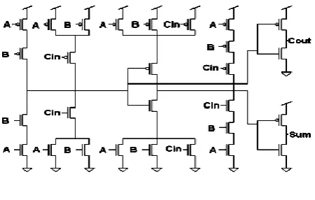
c. CPL logic full adder
Fig.4.CPL Full Adder
V. PRIOR WORK
The full adder operation can be stated as follows: Given the three 1-bit inputs A, B, and Cin, it is desired to calculate the two 1-bit outputs Sum and Carry, where
Sum = (A xor B) xor Cin Cout = A and B + Cin (A xor B)
FIG.5. 1-Bit 8T Full Adder
Figure5 shows the circuit of eight tansistor 1-bit full adder cell. The Sum output is basically obtained by a cascaded exclusive OR of the three inputs. Cout module is implemented using 2T Multiplexer [12]. It is quite evident from Figure5 that two stage delays are required to obtain the sum output and at most two stage delays are required to obtain the carry output.
VI. FULL ADDER SCHEMATICS USING DSCH2 TOOL
Fig6. PTL logic Full Adder
Figure7 shows the CPL logic full adder with 22 transistor counts. The schematics provide transistor counts and timing diagram of the circuit based on dsch2 tools.
Fig7.CPL Logic Full Adder
VII.FULL ADDER LAYOUT USING MICROWIND3.1 TOOL
Microwind is a tool for designing and simulating circuits at layout level. The Microwind program allows the student to design and simulate an integrated circuit at physical description level.
Fig8. Layout of PTL Logic Full Adder
Width 12µm Length 9µm
Fig9. Layout of CPL logic Full Adder
Width 19µm Length 10µm
VIII.RESULTS AND CONCLUSION
Fig10. Waveform of PTL Adder
Fig11. Waveform of CPL Adder
IX.CONCLUSION
Various adders are compared with power, area and delay of most VLSI design parameters. In these different adders our proposed XNOR/XNOR adder-based cell achieves better performance in terms of power dissipation, propagation delay, area, due to less critical path compared to other logic circuits. Transistor count is also an important role of power dissipation and chip area. Reduced transistor count will reduce chip area, supply voltage, power dissipation, power delay product also calculated.
X.FUTURE WORK
REFERENCES
1. Behrooz Parhami, Computer Arithmetic Algorithms and Hardware Designs, Oxford University Press, ISBN 0-19-512583-5, 2000.
2. F.Frustaci, M.Lanuzza, P.Zicari, S.Perri, P.Corsonello, Design high-speed adders in power constrained environments, IEEE Transactions (2009)172–176.
3. Menon R., Kiran C.M., "Concomitant presentation of alopecia areata in siblings: A rare occurrence", International Journal of Trichology, ISSN : 0974-7753, 4(2) (2012) pp.86-88.
4. C.Senthilpari, Ajay Kumar Singh, K.Diwakar, Design of 56 a low power, high performance, 8_8 bit multiplier using a Shannon ba sed adder cell, Micro- electronics Journal39(2008)812–821.
5. Rayen R., Hariharan V.S., Elavazhagan N., Kamalendran N., Varadarajan R., "Dental management of hemophiliac child under general anesthesia", Journal of Indian Society of Pedodontics and Preventive Dentistry, ISSN : 0970-4388, 29(1) (2011) pp.74-79.
6. Swaroop Ghosh, Kaushik Roy, Exploring high-speed low-power hybrid arithmetic units at scaled supply and adaptive clock-stretching, ASPDAC 2008 (2008) 635–640.
7. A.Donald, Neamen„„Microelectronics: Circuit Analysis and Design‟‟, third international ed.,2007, pp.137–139,ISBN:007-125443-9.
8. Shanthi B., Revathy C., Devi A.J.M., Subhashree, "Effect of iron deficiency on glycation of haemoglobin in nondiabetics", Journal of Clinical and Diagnostic Research, ISSN : 0973 - 709X, 7(1) (2013) pp.15-17.
9. S.Goel, A.Kumar, M.Bayoumi, Design of robust, energy-efficient full adders for deep-sub micrometer design using hybrid CMOS logic style, IEEE Transactions on VLSI Systems14 (12)(2006)1309–1321.
10. Chip-Hong Chang, JiangminGu, MingyanZhang, A review of 0.18-mm full adder performances for tree structured arithmetic circuits, IEEE Transactions on Very Large Scale Integration (VLSI) Systems 13(6)(2005)686–695.
11. Sharmila S., Rebecca L.J., Saduzzaman M., "Effect of plant extracts on the treatment of paint industry effluent", International Journal of Pharma and Bio Sciences, ISSN : 0975-6299, 4(3) (2013) pp.B678-B686.
12. V.Muthukumar, B.Radhakrishnan, H.Selvaraj, Multiple voltage and frequency scheduling for power minimization, Journal of Systems Architecture 51(2005) 6–7, ISSN1383-7621.
13. Massimo Alioto, GaetanoPalumbo, “Analysis and comparison on full adder block in sub micron technology”, IEEE Transactions on Very Large Scale Integration (VLSI) Systems 10(6)(2002)806–823.
14. Jeyanthi Rebecca L., Dhanalakshmi V., Sharmila S., "Effect of the extract of Ulva sp on pathogenic microorganisms", Journal of Chemical and Pharmaceutical Research, ISSN : 0975 – 7384 , 4(11) (2012) pp.4875-4878.
15. B Karthik, TVUK Kumar, MA Dorairangaswamy, E Logashanmugam, Removal of High Density Salt and Pepper Noise Through Modified Cascaded Filter, Middle East Journal of Scientific Research, 20(10),pp 1222-1228, 2014.
16. Daimiwal, Nivedita; Sundhararajan, M; Shriram, Revati; , Applications of fMRI for Brain MappingarXiv preprint arXiv:1301.0001, 2012. 17. Daimiwal, Nivedita; Sundhararajan, M; Shriram, Revati; , Respiratory rate, heart rate and continuous measurement of BP using PPGIEEE
Communications and Signal Processing (ICCSP), 2014 International Conference on, PP 999-10022014.
18. Kamatchi, S; Sundhararajan, M; , Optimal Spectral Analysis for detection of sinusitis using Near-Infrared Spectroscopy (NIRS) .
19. Shriram, Revati; Sundhararajan, M; Daimiwal, Nivedita; , Human Brain Mapping based on COLD Signal Hemodynamic Response and Electrical NeuroimagingarXiv preprint arXiv:1307.4171, 2013