A LED Driver Design based on Fly-back
Convert without Auxiliary winding
Pengcheng Xu
1,
Zhigang Han
2Master Student, Dept. of Electronic Science and Technology, Tongji University, Shanghai, China 1 Associate Professor, Dept. of Electronic Science and Technology, Tongji University, Shanghai, China 2
ABSTRACT: For boosting and taking advantage of itsmany outstanding advantages, LED needsespecially designed power supplies driver. Based on fly-back convert topology, a LED driver design is proposed but without auxiliary winding. According to the fly-back ampere-turns ratio conservation, the peak current through secondary side can be specified. The ratio of the interval time of secondary side flowing current to the switching period can also be set under performance of Zero Cross Detection schematic. In the role of filter and charge conservation, the output drive current will be constant. A more stable operation condition can be controlled by limiting the maximum and minimum interval time of secondary side flowing current. The elaborate adjust circuit in ZCD can magnify the resonance signal for better catching ring signal. Simulation results meet the schematic theoretical analysis and design specification.
KEYWORDS: LED,power supply, fly-back, auxiliary winding, ZCD
I. INTRODUCTION
Light Emitting Diode (LED) is widely used in vehicles and traffic lights, house and street lighting, commercial signs and so on. By concerning its outstanding characteristics, like high theoreticalluminous efficacy, long lifetime, environmentally friendly, chromatic variety, LED will be the trend in lighting[1].
For boosting and taking advantage the aforementioned advantages, LED need new power supply topology especially designed for them. In general, LED driver uses photoelectric couple in secondary side feedback solutionor auxiliary winding in primary side feedback solution to detect drivecurrent. Inevitability, it reduces the effect of isolation which has been widely used in LED driver for safety and both raises the manufacturing cost accordingly[2,3].
Based on the fly-back ampere-turns ratio conservation, the peak current on secondary side can be specified. The ratio of the interval of secondary side flowing current to the switching period can also be achieved under performance of Zero Cross Detection schematic. In the role of filter and charge conservation, the output drive current is constant. A more stable operation condition can be controlled by limiting the maximum and minimum time of secondary side flowing current. The elaborate adjust circuit in ZCD magnify the resonance signal[4,5].
II. FLY-BACK TOPOLOGY
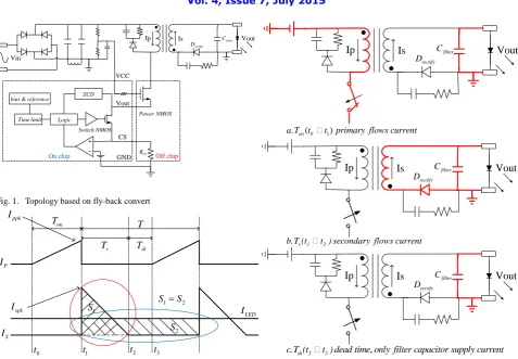
Fig.1 shows the topology schematic based on fly-back converter used in the proposed driver design. Itconsists of Rectifier Bridge, power up capacitor, fly-back transformer without auxiliary, filter capacitor, and RCD for absorption peak pulse. The off chip Power NMOS is for its parasitic capacitors Cdssand Cgsswhich is vital in resonance for Zero
Cross Detection (ZCD). The on chip Switch NMOS can be used to turn on or turn off the primary current. The energy stored in transformer is delivered to secondary load side in each cycle[6,7,8,9].
There are three different current states in discontinuous mode fly-back converter. As depicted in Fig.2 (a), when Switch NMOS turns on, except bridge diodes,all rectifier diodesbecome reverse-biased, and alloutput load currents are supplied from the output filter capacitors. The transformer acts like apure inductor and primary current builds up linearly in it to a peak value. When Switch NMOS turns off, all winding voltages reverse under fly-back action, bringingthe output diode into conduction and the primary stored energy 2
1 2L IP ppk isdelivered to the output to supply load current and replenish
Vout
Vin
Ip Is
CS Vout
GND VCC
Logic
ZCD
CS
R
Power NMOS
Switch NMOS
On chip Off chip
filter
C
rectify
D
Time limit
&
bias reference
Fig. 1. Topology based on fly-back convert
Vout
Ip Is
Vout
Ip Is
Vout
Ip Is
filter
C
rectify
D
filter
C
rectify
D
filter
C
rectify
D
1
. on(0 )
a T t t primary flows current
r 1 2
b.T (t t ) secondary flows current
2 3 ,
dt
c.T (t t ) dead time only filter capacitor supply current
Fig. 2. Different current flowing states in fly-back converter
LED
I
spk
I
ppk
I
0
t t1 t2 t3
on
T
r
T Tdt
T
1
S
2
S
1 2
S S
P
I
S
I
Fig. 3. Waveforms of DCM fly-back converter current
In the proposed solution, the secondary side current drops to zero before the startof the next turn on period of Switch NMOS, as depicted in Fig.2 (c). It also called discontinuous current mode (DCM) or complete energy transfer mode. The rules for an inductor withmore than one winding are as follows:The primary to secondary ampere-turns ratios is conserved.
NpIppk NsIspk (1) It follows thatI I N /N
spk ppk p s (2)
III.PRINCIPLE OF CONSTANT DRIVE CURRENT
As depicted in Fig.3, the output current ILED is an average value for the area of S1 distributed uniformity on the region
of
2
S in an entire period T under the influence of filter capacitorCfilter.That is,
1
2IspkTr ILEDT(3)
By combining Eq. (2), consequently, 1( / ) ( / ) 2
Switch NMOS Primary side
Turn off NMOS _
ref CS V
CS R CS
V
ppk I
CS V
_
ref CS V P
I on T
Fig. 4. Schematic of specify primary peak current
_
refCS
V S
R Q
S
R Q
_time
ref
V VCC
Switch NMOS Power NMOS
time V
CS
V
P
I
CS
R
time
C
c
I
d
I
S
V _ min _ max
r r r
T TT
!
YES
!
NO
on_ min on on_ max T T T
!
YES NO!
Bandgap Reference
ZCD
Q
compe
nsat
ion
Fig. 5. Schematic of timing control
/
Np Ns is depend on the physics structure of the fly-back transformer, and it can be concerned a constant value. A
constant output drive current can be obtained if the I
ppk and Tr/Tare also specified in the proposed solution. These
can be achieved by the primary-side feedback without auxiliary winding, but using a voltage coupled network circuit to specify the ratio T /T
r and a current sense circuit to set the peak primary current Ippk.Based on above discussion, the
two decisive factors for constant output drive current is the primary peak current I
ppk and ratio of duration of secondary
side flowing current to periodTr/T.
IV.SPECIFY PRIMARY PEAK CURRENT AND THE RATIO
As discussion above, under the fly-back convert topology, the constant drive current depends the peak primary current
ppk
I and the ratio of duration of secondary side flowing current Trto the entire switching period T . A. Specify the peak primary current
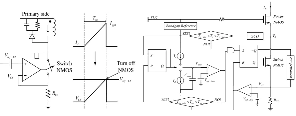
The primary peak currentIppkcan be specified by Current Sense circuit which is depicted in the following Fig.4. When
primary current IPreaches to specified peak valueIppkduring Switch NMOS turns onTon, current sense voltage VCS across sampling resistor RCSwill rise to reference voltage Vref_CS. At the same time, voltage comparator shut down Switch NMOS.That is,
_
ref CS
ppk
CS
V
I
R
(5)
_
ref CS
P spk
S CS
V
N
I
N
R
(6)B. Specify the ratio of duration of secondary side flowing current to the switching period
This can be achieved by Timing Control Logic circuit, as depicted in Fig.5. Based on the work ofWeidongNieet al [10], a timing control with time checking function and cable compensation is proposed. The time checking circuit can make sure the entire system operate in a stable conduction by limiting the interval time of secondary conducting
_ min _ max
r r r
checking will be explained in next section.After the voltage
V
timeacross the timing capacitorC
timewithin charging state rises to the reference voltageV
ref_time, Switch NMOS will be turned on.At the same, primary conducting currentincreases linearly with a slope
V
inL
P. HereV
inis the rectified input voltage._
ref time
V
time_ max
V
time_ min
V
time
V
P
I
S
I
on
T Tr Tdt
1
r
T Tr2
0
t t1 t2 t3
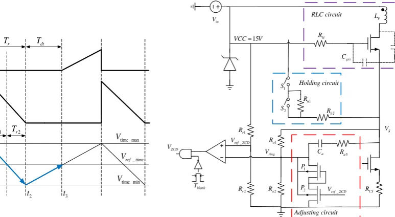
Fig. 6. Waveform of voltage across timing capacitor
P
L
dss
C
gss
C
1 S
2 S
S
V
_
ref ZCD
V 1
r
R
2
r
R 1
a
R
2
a
R
1
h
R
G
R
15
VCC V
ring
V
ZCD
V
blank
T
CS
R _
ref ZCD
V 2
h
R
3
a
R
a
C
1 P
2 P
in
V
Adjusting circuit RLC circuit
Holding circuit
Fig. 7. Zero cross detection schematic
As illustrated above, the Current Sense circuit can specify the primary peak current
I
ppk. So when current sense voltageCS
V
reaches to the setting reference pointV
ref_CS, the timing capacitor will be switched to discharging state. Thetermination of interval
T
ris depended on ZCD. At the moment when secondary current decreases to zero, the drain of Power NMOS will lost part voltage and a resonance will occur for RLC circuit consisted by primary inductanceL
P, parasitic capacitorC
dss and gate resistorR
gate .Only after timing capacitorC
timeis recharged andV
time climbs to_
ref time
V
, a new cycle begin with turning on Switching NMOS.The charging or discharging current of timing capacitor
I
c andI
d are mirrored from a same current source for1
c ref
I
I
andI
d
2I
ref .The duration of Switching NMOS turning onT
on can be expressed astime_ max _
(
ref time)
timeon
c
V
V
C
T
I
(7)Secondary side conducting current during
T
r andT
r
T
r1
T
r2, wheretime_ max _
1
(
ref time)
timer
d
V
V
C
T
I
(8)_ time_ min
2
(
ref time)
timer
d
V
V
C
T
I
From the zero cross of secondary side current to starting another new cycle, the dead time can be depicted as
_ time_ min
(
ref time)
timedt
c
V
V
C
T
I
(10)The each period is
time_ max time_ min
1 2
(
)
1
1
(
)
on r dt
time
ref
T
T
T
T
V
V
C
I
(11)And the dead time can be expressed as
1 2
time_ max time_ min
2
(
)
1
r r r
time
ref
T
T
T
V
V
C
I
(12)So the ratio of secondary side conducting duration
T
rto the periodT
can be obtained1
1 2
r
T
T
(13)In conclusion, a constant LED drive current can be achieved with a specified primary peak current
I
ppkand the ratio ofr
T
to theperiodT
, and be given by:_ 1
1 2
1
2
p ref CS
LED
s CS
N
V
I
N
R
(14)V. ADJUST RESONANCE RING SIGNAL
For detecting the time point of secondary side current reaching to zero, Zero Cross Detection (ZCD) circuit is elaborated designed. As shown in Fig.7, ZCD sensing circuit consists of a resonant RLC circuit, Holding circuit, and Adjusting circuit.
A. RLC resonance circuit
During dead time interval
T
r, secondary side currentI
sdrops linearly from peak valueI
spk.The drain voltageV
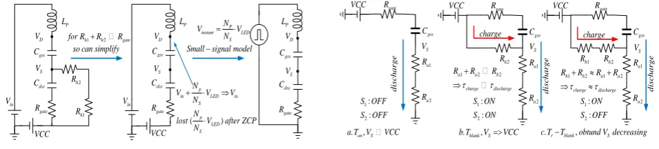
DofVCC in V P L gss C dss C gate R 2 h R 1 h R S V 1 2
h h gate
for R R R
so can simplify
VCC P L gss C dss C in V ( ) p in LED in
S p
LED S
N V V V
N N
lost V after ZCP N
gate
R
Small signal model
gss C dss C gate R P instant LED S N V V N
LP
D
V VD
S V D V S V
Fig. 8. Resonance caused by RLC
1 a R 2 a R gate R VCC 2 h R gss C 1 h R
1 2 1 2
h h a a
charge discharge
R R R R
1 a R 2 a R gate R VCC 2 h R gss C 1 a R 2 a R gate R VCC gss C S
V VS VS
. on, S
a T VVCC b T.blank,VSVCC c T.rTblank,obtund V decreasingS
d isc h a rg e charge charge
1 2 2
a a h
charge discharge
R R R
1 2 : : S OFF S OFF 1 2 : : S ON S ON 1 2 : : S ON S OFF d isc h a rg e d isc h a rg e
Fig. 9. Hold circuit under different states
A damped oscillation voltage at drain node of Power NMOS can be expressed as,[10]
( )
P tcos(2
)
D LED r
S
N
V t
V
e
f t
N
(15)where
2
G PR
L
,1
2
r P df
L C
, 01
P d
L C
,C
sum
C
dss
C
gss.A useful parameter is the damping factor,
which is defined as the ratio of
to
0,0
2
G d PR
C
L
(16)The special case of ζ = 1 is called critical damping and represents the case of a circuit that is just on the border of oscillation. It is the minimum damping that can be applied without causing oscillation. Under the reason, the design should guarantee ζ>1.
So the source voltage
V
Sexperiences a voltage change
V
S(t)
during resonant period which can be given by( )
(
/ /
) (
)
( )
S G G D
dss gss dss
j
j
j
V t
R
R
V t
C
C
C
Where
=2
f
r.If G/ /
dss gss
j
j
R
C
C
=
,(t)
SV
can be simplified as( )
21
( )
(
)
S D
dss gss dss
V t
V t
C
C
C
(17)B. Holding circuit
Holding circuit which is consisted by two MOSFET switches and two resistors helps to set a proper DC voltage for
V
S before resonance occurring. The purpose of Hold circuit is to obtund the decrease ofV
S during(
T
r
T
blank)
after charged toVCC
in the blanking period. Before the secondary side current decreasing to zero, a proper voltage ofV
S should be set for compared with reference voltageV
ref_ZCDafter divided. If without Hold circuit, the voltageV
SThe purpose of keeping a resistors network consisted by
R
h1 andR
h2 is to obtund the decrease ofV
S during(
T
r
T
blank)
after increasing toVCC
during blanking time.If without the resistors network consisted by
R
h1andR
h2, which can be achieved by open theS
1andS
2both, the decreases ofV
Sduring(
T
r
T
blank)
can be given by/
(1
t)
S
V
VCC
e
(18)Where
(
R
g
R
3
R
4)
C
gss.Under this circumstance, if unfortunately
V
S drop toV
ref_ZCDbefore zero cross of secondary side current will cause logic error.With Hold circuit performance, as depicted in Fig.9 (c),C
gssexperiences a discharger and charge both and,/
1 2
1 2 1 2
(1
t)
h h
S
a a h h
R
R
V
VCC
e
R
R
R
R
(19)Where
[
R
G
(
R
h1
R
h2) / /(
R
a1
R
a2)]
C
gss, andt
T
rT
blank.At
t
t
2 ,V
S
VCC
V
S. At this time, the divider voltageV
resonant must be higher thanV
ref_ZCD . Otherwise the ZCD sense circuit will output a signal to indicate a ZCD signal, although there is no ZCD signal in fact.C. Adjusting circuit
For taking the input scope op comparator into concerned,
V
Sshould be divided into a suitable value for compared. So the resistorR
a1usually is very larger, even larger enough to damp the resonant seriously. At the worst situation, although there is ringing happened onV
S, the voltageV
resonantcannot be detected with resonant signal and an error happened.To avoid it, the Adjusting circuit is proposed in the ZCD schematic. It is consisted by an ResonanceMagnify RC and Carriers Release PMOS, as depicted in Fig.07.The Body of each Release PMOSs is connected to
V
resonantbut notVCC
. After intervalT
on, the Switch NMOS is turned off. Due to the leakage inductance of transformerand the parasitic capacitance of Power NMOS, the ringing occurs.If unfortunately, the ring is larger enough to be missed consider as ZCD signal, the system will be fail for logic error.IfV
resonant
V
ref_ZCD
V
thPduring the ringing, the Release PMOS can be turn on and release the carriers for weaken the unintended ringing.During the ZCD resonant, the RC magnify circuit can deliver the ringing through its RC. A more explicit ZCD can be transformed to the comparator.By using complex resistor concept, the whole resistors can be expressed as,
1
2
1
1
=
1
a
j a
sum a eq eq
a
a
R
j C
Z
R
R
jX
Z e
R
j C
(20)
where 2 1 2
1
(
)
1
a
eq a
a a
R
R
R
C R
,2 1 2 1
(
)
1
a a
eq
a a
C R
X
C R
,2 2
eq eq
Z
R
X
,tan
1 eqeq
X
R
.
the DC part of
V
ringcan be expressed as _ 21 2
a
ring DC S_DC
a a
R
V
V
R
R
(21)And AC part of
V
ring is depicted follow, ring_AC a2 S_ACall
R
V
V
Z
(22)If without the ring magnify capacitor
C
a, _ 2 _1 2
a
ring AC S AC
a a
R
V
V
R
R
(23)For 2 2
1 2
a a
all a a
R
R
Z
R
R
, the Adjusting circuit can magnify the ring from original version.VI.TIME CHECKING AND COMPENSATION
A. Time checking
For a stable and precision operation condition, the duration time
T
rof Secondary side flowing current should be limited in a certain scope. Unusually larger or smaller of dead timeT
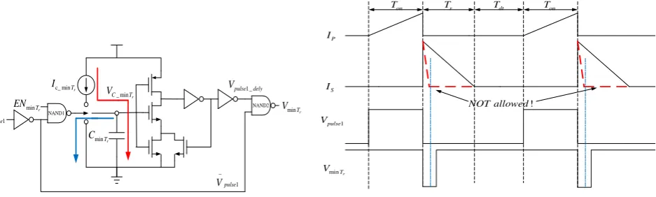
r are both not allowed in this proposed schematic system.Confining the minimum
T
r schematic is shown in Fig.10.minTr
C
1
pulse
V minTr
V
minTr
EN
c_ minTr
I
1
pulse V
1_
pulse dely V
NAND2 NAND1
_ minr
C T
V
Fig. 10. Confining the minimumTr
P
I
S
I
1
pulse
V
minTr
V
on
T Tr Tdt Ton
! NOT allowed
Fig. 11. Wareform of confining the minimum Tr
During in the interval
T
on primary side flowing current, the low level signal “0” voltageV
pulse1 will closes the NAND2 outputting a high level signal “1”. When Switching NMOS is shut off, the energy stored in the transformer will be transformed to secondary side while current
I
slinearly descend from the peak currentI
spk. As depicted in Fig.,V
pulse1switch to low level signal “0” lead the voltage min
r
T
V
turning over to “0”, and also through two inverses the low level signal “0” from output of NAND1 result in the capacitor minr
T
C connectingto the current source _ min
r
c T
I .
The current _ min
r
c T
I charges capacitor CminTr
and the voltage _ min
r
C T
V increase linearly until reaching to the threshold voltage
thN
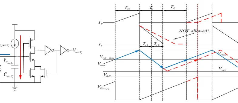
maxTr
C
1
pulse
V
maxTr
V
maxTr
EN
c_ maxTr
I
NAND1
maxTr C
V
Fig. 12. Confining the maximum Tr
_
ref time
V Vmax
min V
time
V
P
I
S
I
thN
V
on
T Tr Tdt
!
NOT allowed
1
r
T Tr2
max_Tr
C
V
Fig. 13. Wareform of confining the maximum Tr
Only after the voltage crossing min
r
T
C
larger enough to turn on the NMOS, _ minr
C T
V
can return to high level signal “1”. So the duration time of minr
T
V
being on “0” can be expressed as,minT min
_ min
r r
r
thN
T
c T
V
t
C
I
(24)Confining the maximum
T
r schematic is shown in Fig.12.As discussion above, When Switching NMOS is shut off, energy stored in the transformer will be transformed to Secondary side while
I
slinearly descend fromI
spk. As depicted in Fig.12,V
pulse1will switch to “0” then the low level signal “0” from output of NAND1 allow current source _ maxr
C T
I
change the capacitor maxr
T
C
. The voltagemaxTr
C
V
across max
r
T
C
increaselinearly, until beginning of a new cycle. If unfortunately, the duration timeT
r is so long evenmaxTr
C
V
up toV
thNcasing a turning over on voltage signal maxr
T
V
.So the maximum duration time of
T
rcan be expressed as,min
maxT max ti min g
_ mxx _timing
r r
r
thN
T
c T c
V
V
t
C
C
I
I
(25)The process of checking of Switching NMOS turning on time
T
onis similar withT
r. Dut to space constrains, it does’t give detail in this paper.B. Cable compensation
com
V
com
I
com
C
com
R
ref
I
2
pulse
V
P
I
CS
R
CS
V
P
I
com
I
CS
V
com
P
com
N
Fig. 14. Cable compensation schematic
During Switching NMOS turning on, the pulse voltage is a signal “1” shutting down the PMOS. After that, the carries storing in the capacitor will be decreased through mirrored current form reference current. Accordingly, the voltage across capacitor linearly decreases causing compensate current reducing at the same time. So a higher primary peak current will get a smaller compensatory current.
VII. SIMULATION RESULTS AND CONCLUSION
The proposed LED driving IC is implemented in Shanghai Huahong 1um5V/40V CMOS process. It is used Cadence Spectre to simulate the schematic.
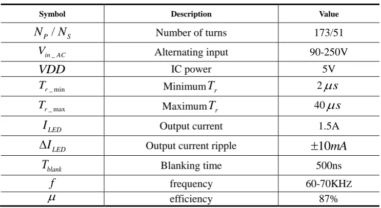
TABLE I. CIRCUIT PARAMETERS
Symbol Description Value
/
P S
N
N
Number of turns 173/51_
in AC
V
Alternating input 90-250VVDD
IC power 5V_ min
r
T
MinimumT
r 2
s
_ max
r
T
MaximumT
r 40
s
LED
I
Output current 1.5ALED
I
Output current ripple
10
mA
blank
T
Blanking time 500nsf
frequency 60-70KHZ
efficiency 87%P
I
S
I
ring
V
time
V
o n
T Tr
dt
T
ZCP signal need block
Fig. 15. A set ratio Tr/Tsimulation
pulse V
com
V
com
I
P
I
on
T
compensatory current
primary peak current
Fig. 16. Current compensation simulation
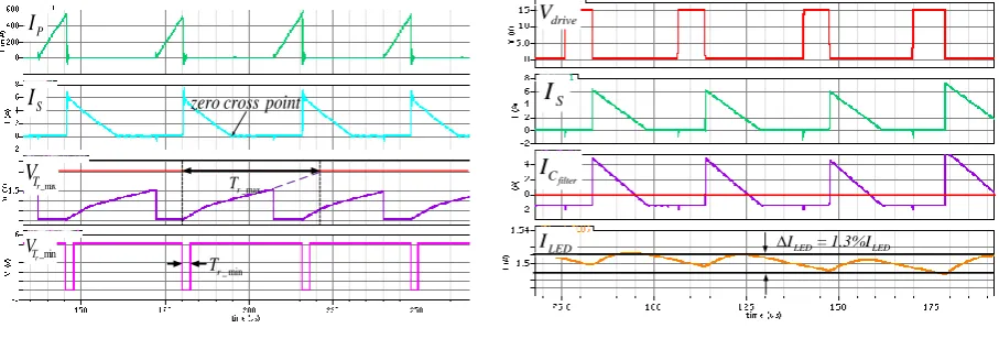
As depicted in Fig.15, due to leaking inductance, a resonance occurs during switching NMOS converting from turning on to turning off. This ring signal can be wrong regarded as zero cross point. A 500ns blanking time has been set to eliminate this influence. After secondary side current dropping down to zero, for RLC circuit, a resonance occurs. And Zero Cross Detection schematic will check this ring and timing voltage rising again. In Fig.16, the compensatory current adds to the primary peak current for decreasing cable drop influence.
P I
S
I
_min
r T
V
_ min
r
T _max
r
T _max
r
T
V
zero cross point
Fig. 17. Time checking simulation
drive
V
S
I
filter
C I
LED
I ILED= 1.3%ILED
Fig. 18. Output current simulation
As depicted in Fig.17, the secondary side flowing current duration time Tr is limited between 2us and 40us for generating the system operation stability. In Fig.18, a constant LED driving current with 1.3% ripple is achieved. The simulation result shows the proposed LED driver design based on fly-back topology without auxiliary can achieve a constant output current. ZCD can detect the point of secondary current dropping to zero and set a constant ratio or Trto period T.Time checking schematic limits the scope of Trand make the system operates in stable conduction. Besides, the cable compensation improves the precise of constant output.
REFERENCES
[1] Manuel Arias, Aitor Vázquez, Javier Sebastián. An Overview of the AC-DC and DC-DC Converters for LED Lighting Applications [J]. AUTOMATIKA, 2012, 53(2): 156–172.
[2] H. Vender Broeck, G. Sauerlander, and M. Wendt, Power driver topologies and control schemes for LEDs [C]. Twenty Second Annual IEEE Conference on Applied Power Electronics Conference, Anaheim, CA, USA,2007: 1319–1325.
[4] W. Kleebchampee, C. Bunlaksananusorn, Modeling and Control Design of a Current-Mode Controlled Flyback Converter with Optocoupler Feecdback [C], International Conference on Power Electronics and Drives Systems. Kuala Lumpur. 2005:787-792
[5] Y. W. Q. Z. Tingzhang Liu, Jingjie Shen, Constant Current LED Driver Based on Flyback Structure with Primary Side Control [C]. Power Engineering and Automation Conference, 2011, pp. 260–263, Sep. 2009.
[6] Junming Zhang, Hulong Zeng, Ting Jiang, A Primary-Side Control Scheme for High-Power-Factor LED Driver With TRIAC Dimming Capability [J], IEEE TRANSACTIONS ON POWER ELECTRONICS,2012,27(11):4619-4629
[7] Tzuen-Lih. Chern, Li-Hsiang Liu, Ping-Lung Pan et al. Single-stage flyback converter for constant current output LED driver with power factor correction [C]. 4th IEEE Conference on Industrial Electronics and Applications,Xi'an, 2009: 2891–2896.
[8] A. L Pressman, K. Billings and T. Morey, Switching Power Supply Design, 3rd ed [M]. New York: McGraw Hill Professional, 2009:117-146 [9] R.JACOB BAKER. Circuit Design, Layout, and Simulation, Third Edition [M]. United States of America, IEEE Press,2010:116-118
[10] Weidong Nie, Jin Wu, Zongguang Yu. A simple cost-effective PSR LED driver without auxiliary winding [J].IEICE Electronics Express, 2013,10(23):1-9
[11] Tsung-Hsiu Wu, Quasi-resonant fly-back converter without auxiliary winding [P], America:US20080278974, Mar.2011
BIOGRAPHY
Pengcheng Xu currently pursuits his Master Degree on Integrated Circuit Engineering at Tongji University. He received his Bachelor Degree from Shanghai Normal University, China, in July 2013. In 2014, he was honored with National Graduate Student Scholarship inChina. His research areas are analog integrated circuit design and switching power supply deriver design. Pengcheng Xu is with the Department of Electronic Science and Technology, Tongji University, China, Shanghai, 201804 CN, E-mail:[email protected].