ABSTRACT
SCOTT, JOSHUA IRVIN. Characterization of Mechanical and Electrical Properties of Polymer Semiconductor Blend Films. (Under the direction of Dr. Brendan O’Connor).
Polymer semiconductors based on donor-acceptor monomers have recently resulted in
significant gains in field effect mobility in organic thin film transistors (OTFTs). To promote
charge transport, these polymers have incorporated fused aromatic rings and have been
designed with planar backbones, favorable π-π stacking, and strengthened intermolecular
interactions which result in stiff and brittle films. These materials typically require complex
synthesis which can result in increased production costs. Thus, developing methods to improve
mechanical behavior while lowering material consumption during fabrication will significantly
improve opportunities for adoption in flexible electronics. To achieve these goals, we consider
blending a brittle high-performance donor-acceptor polymer
poly[4(4,4dihexadecyl4H-cyclopenta[1,2b:5,4b’]dithiopen2yl)alt[1,2,5]thiadiazolo[3,4c]pyridine] (PCDTPT) with
ductile regioregular poly(3hexylthiophene) (P3HT). We find that the ductility of the blend film
is significantly improved compared to neat PCDTPT films, and when the film is employed in
an OTFT the performance is largely maintained. The ability to maintain charge transport
characteristics is achieved due to vertical segregation within the blend, while the improved
ductility is achieved due to partial miscibility of the polymers. Applying large strains to the
ductile films is shown to orient both polymers. The strained films can then be employed to
increase charge carrier mobility. These results highlight material opportunities for high
© Copyright 2015 by Joshua Irvin Scott
Characterization of Mechanical and Electrical Properties of Polymer Semiconductor Blend Films
by
Joshua Irvin Scott
A thesis submitted to the Graduate Faculty of North Carolina State University
in partial fulfillment of the Requirements for the Degree of
Master of Science
Mechanical Engineering
Raleigh, North Carolina
2015
APPROVED BY:
Dr. Mohammed Zikry Dr. Matthew Bryant
ii
DEDICATION
I dedicate this work to my loving wife Cassie who has given me constant guidance
throughout these long two years. I would also like to express a special feeling of gratitude to
my parents, Holly and Irvin Scott who have always supported me during all of my endeavors
within and outside the realm of academics. Finally, I would like to thank my brother Matt
iii BIOGRAPHY
Joshua Scott was born in York, Pennsylvania to his parents Holly and Irvin Scott and raised
with his brother Matthew. He graduated from Red Lion Area Senior High School in 2009.
He then attended Shippensburg University of Pennsylvania for his undergraduate study.
While attending Shippensburg he had the honor of playing on the inter-collegiate baseball
team and the distinct privilege of being a member of the 2013 team that went to the college
world series. He graduated with his Bachelor of Science in Physics with a minor in
Mathematics in 2013. He was then admitted to the North Carolina State University graduate
program in 2014 to pursue a Master’s degree in Mechanical Engineering with a research
focus on mechanical and electrical properties of semiconductor polymer blends. In August
of 2015 he married his long-time girlfriend Cassie Scott and the two of them currently live
iv
ACKNOWLEDGEMENTS
I would like to express my sincere gratitude to my advisor Dr. O’Connor for his continuous
guidance and knowledge that helped me during research and in the writing of this thesis. I
would also, like to thank all of my research group members and those who have helped me
with this research Nrup Balar, Pratik Sen, Tianlei Sun, Xiao Xue, Dr. Omar Awartani, Ethan
Edwards, Gillian Coats and Ben Hoffman. You kept me on my toes and made life in the lab
v
TABLE OF CONTENTS
LIST OF FIGURES……..………..………...vi
1. INTRODUCTION……….………..1
1.1 Motivation and Background……….……….……….………..1
1.1.1 History……….………….………1
1.1.2 Polymer Blends……….….………..4
1.2 Device Physics of OFETS………..………..10
1.2.1 Organic Polymers……….………..10
1.2.2 Transistors……….……….14
2. MULTI-COMPONENT POLYMER FILMS TO SIGNIFICANTLY INCREASE DUCTILITY OF HIGH PERFORMANCE POLYMER SEMICONDUCTORS..……….…….……….………..17
2.1 Introduction and OTFT performance…….……..…….……….……..17
2.2 Film Morphology……...……….………….………21
2.3 Film Ductility……….……….……….29
3. SUMMARY...……….………..………..35
3.1 Conclusions……….……….……….35
3.2 Future Work...……….………….………37
vi
LIST OF FIGURES
1. INTRODUCTION
Figure A Device Degradation from Blending with Insulating Polymers………....5
Figure B Mechanical Improvement through Blending………...………...6
Figure C PCBM concentration as a Result of Surface Energy Considerations………..7
Figure D Segregation Caused by Solubility Differences…………..………...………..9
Figure E Lateral Segregation from Solvent Evaporation………..………..…..9
Figure F Model of sp2 hybridization………..……….12
Figure G Diagram of HOMO and LUMO Levels………..….13
Figure H Semiconductor Band Diagram………..………...15
Figure I Field-effect Transistor Architectures………..…...16
2. MULTI-COMPONENT POLYMER FILMS TO SIGNIFICANTLY INCREASE DUCTILITY OF HIGH PERFORMANCE POLYMER SEMICONDUCTORS Figure 1 Optical Microscope Image of PCDTPT..…...………..…18
Figure 2 Transfer Curves of Unstrained 5μm Devices/Channel Length Dependence.….…..20
Figure 3 Optical Comparison of Unstrained and 75% Films…...………...22
Figure 4 AFM Comparison of Unstrained and 75% Strained 1:1 and 1:4 Films....………....23
Figure 5 TOF-SIMS Results………...………....24
Figure 6 XPS Results………...………...26
Figure 7 UV-VIS Absorbance with Light Parallel to Strain………...27
Figure 8 GIXD Images of Crystal Orientation..……….28
Figure 9 AFM Comparison of 25% and 50% 1:1 blend film..………...30
Figure 10 Absorbance Anisotropy…...………...31
Figure 11 Dichroic Ratio of 1:1 and 1:4 by Wavelength………...…...…………..32
Figure 12 Mobility of 5μm Devices with Strain………...………….….33
1 1. INTRODUCTION
1.1Motivation and Background 1.1.1 History
Historically, the first FET was proposed and patented by Julius Edgar Lilienfeld an
Austrian-Hungarian physicist in 1925, who described his patent as “Method and apparatus for
controlling electric current”. It wasn’t until 1959 that Dawon Kahng and Martin Atalla of Bell
Laboratories invented and executed the metal oxide semiconductor field-effect transistor most
commonly known as a MOSFET. The MOSFET has the ability to operate with very little
current giving it a critical advantage over other transistors making the MOSFET the most
common transistor in both digital and analog circuits. In 1977 Heeger, MacDiarmid, and
Shirakawa discovered conductive polymers by exposing polyacetylene to chlorine, bromine,
and iodine vapour. They quickly realized that this procedure resulted in an uptake in halogen
and that the conductivity of the polymer is significantly increased at room temperatures. For
this discovery the group was awarded the Nobel Prize in Chemistry in 2000 “for the discovery
and development of conductive polymers”. (Shirakawa 1977) It wasn’t until 1987 that the first
organic field effect transistor based on a polythiophene thin film as the semiconductor was
reported by Tsumura, Koezuka, and Ando of Mitsubishi Chemical achieving a hole mobility
of 2x10⁻⁵ cm2V-1s-1. (Koezuka 1987) This coupled with reports by Tang in 1986 of an organic
heterojunction, a two layer organic photovoltaic cell which achieved power conversion
efficiency values of 1% and fill factor values as high as 0.65. (Tang 1986) As well as the
organic light emitting diode (OLED) by Tang and Van Slyke in 1987 which produced a green
electroluminescence further intensified interest in organic semiconductors. (Tang 1987) The
2
Laboratories in Eindhoven was able to successfully manufacture an all polymer-integrated
circuit making it the first complex organic circuit. (Hu 2012) Since then the interest for organic
electronics has been steadily growing with the demonstration that organic materials could be
used in low cost and flexible applications with relative ease of processing using inkjet printing
or spin coating. (Allard 2008, Forrest 2004, Sirringhaus 2014) This is an inherent advantage
of organic materials as inorganic semiconductors can require expensive and labor intensive
deposition processes including vapor deposition. Along with this, OFET components have
recently been able to achieve field mobility values, 1-10 cm2V-1s-1, approaching that of
amorphous silicon, 0.5-1cm2V-1s-1. (Sirringhaus 2014) Field mobility is a critical parameter
when discussing OFET performance. Commonly recognized as electron mobility in solid-state
physics this nomenclature is slightly misleading as in semiconductors the mobility can actually
be achieved and measured with electrons and holes. In general the mobility is the
characterization of how quickly a “charge” can move through a metal or semiconductor. In
field-effect transistors this mobility can be measured in two distinct regimes, saturation and
linear. For the testing done in this work the mobility, μ, is calculated in the saturation regime
with Equation 1.
μ = 100% *( 2∗𝐿𝑊𝐶 ) * S (1)
Where % is the percent of the transistor covered by the semiconductor film, L is the
channel length, W is the channel width, C is the capacitance of the dielectric and S is the max
slope calculated from the gate voltage plotted against the drain current. It is necessary to
include the percent coverage of the film over the electrodes as during the film transfer process
it is common for some of the electrodes to be left only partially covered. These mobility
3
achieved by Koezuka in 1987. Commercially this indicates a real possibility for organic
electronics with decreased production costs. This realization that organic electronics are
feasible has over the past 25 plus years resulted in a race for the synthesis of high performance
polymers that demonstrate excellent levels of charge transport in order to compete and eclipse
their inorganic counterparts. One interesting approach was the synthesis of donor-acceptor
polymers that contain dipolar functionality such as the high performance polymer PCDTPT.
However, in order to increase electrical properties many of these polymers have sacrificed their
mechanical properties by creating strong intermolecular interactions resulting in stiff and
brittle films. This was done by increasing the amount of aromatic rings within the polymer
backbone, synthesizing the polymer such that the backbone is more planar, adjusting the
spacing of the alkyl side chains and creating more efficient π-π stacking. (Biniek 2012) This
is both exciting and unfortunately very inconvenient. Considering charge transport is most
efficient along the polymer backbone the alignment of the chains within a film is often
modified during processing to improve charge transport behavior as well as to gain
morphological information. Anisotropic behavior can be achieved with many different
methods including strain alignment (Gargi 2013, O’Connor 2011), directional solidification
from solvents (Brinkmann 2006, Brinkmann 2007), mechanical rubbing (Sirringhaus 2000,
Tseng 2012), or flow coating (DeLongchamp 2009). In this work, the strain alignment method
will be utilized as it presents several advantages over the other methods including, the ability
to control the levels of strain and thus the relative amount of alignment of the film as well as
the ability to transfer the film onto just about any other substrate post strain. The latter enables
different measurements to be taken with ease as opposed to developing new processing
4
deficient mechanical properties places a limitation on improving the film alignment and charge
transport. This limit in the mechanical properties also limits the type of device structure the
polymers can be utilized in. By increasing ductility a film would be less prone to fracture in
flexible electronic devices making them an attractive option for stretchable and completely
flexible OTFT’s which are greatly desired not only so that the average person can have an
exceedingly large curved television, but within the biomedical community to improve device
comfort. The challenge is therefore to retain the excellent charge transport characteristics of
these polymers while improving the mechanical characteristics.
1.1.2 Polymer Blends
Polymer blends present an intriguing and potentially viable method for meeting the
challenge of improving mechanical characteristics while retaining electrical properties of these
high performance donor acceptor polymers. An advantage of blending polymers over
synthesis techniques is the relative ease at which it can be accomplished. Both polymers only
have to be soluble in a common solvent for processing of the blend to be realized. Some
consideration needs to be taken however when selecting the polymer blend including; the
molecular weight, degrees of crystallinity, crystallinity sequence, and crystallinity kinetics.
These properties can enable the morphology within the film to be preferentially altered and
will be discussed a little later. Historically, polymers with good semiconducting properties
have been blended with inert or insulating polymers which can degrade device performance,
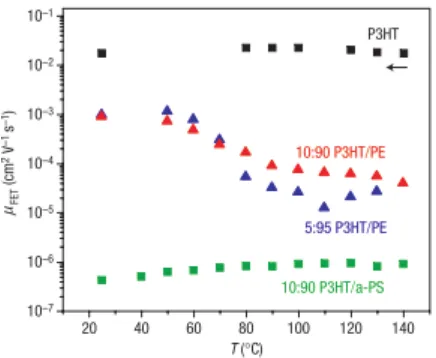
Figure A. (Ferenczi 2011, Goffri 2006, Scaccabarozzi 2014) This can occur through crystallization issues as seen when blending P3HT with polyethylene, PE. Under specific
processing conditions the PE will crystallize before the P3HT in such a way that the P3HT
5
semiconducting polymer responsible for the electrical properties of the blend, not being able
to efficiently crystallize which results in poor electrical performance of the blend.
Figure A. Effect of blending a semiconductor with an insulating polymer. (Goffri 2006) However, it has been shown that blending polymers with an insulator can actually result
in self encapsulation which increases the stability of the device in air which is a highly desirable
characteristic as organic semiconductors are infamous for oxidation with exposure to air which
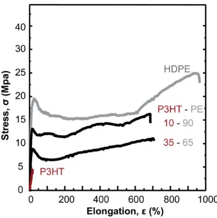
reduces device performance. (Goffri 2006, Ferenczi 2011) Blends have also demonstrated the
ability to combine the advantageous properties of two individual materials for optimization of
6
Figure B. Mechanical improvement by blending the semiconductor P3HT with an insulator polymer PE. (Scaccabarozzi 2014)
Blending two different polymers can result in vertical segregation within the film.
Electrically, if the polymer responsible for charge transport can be segregated to the substrate
surface the charge transport characteristics of the blend will mimic that of the single material.
This is due to the very narrow region that charge transport takes place within these devices,
less than 10 nm from the substrate. (Kline 2006, Salleo 2007) Obtaining preferential vertical
segregation while very complicated has been shown to be controlled with the following
methods: surface treatments, crystallization of components, solvent evaporation, solubility,
and control of the blend composition. (Arias 2006, Campoy-Quiles 2008, Germack 2010,
Heriot 2005, Iyengar 1996, Qiu 2009, Salleo 2002, Shin 2013, Smith 2010) Surface treatments
such as the deposition of self-assembled monolayers, SAMs, can promote vertical phase
segregation by altering the surface energy of the substrate. (Germack 2010) A typical surface
modification for OFETs is the application of an octyltrichlorisane OTS layer to the silicon
7
the surface hydrophobic, which is known to passivate the surface (reduce interface electronic
trap states) and promote a preferential π-π stacking in the plane of the film. Within a binary
blend system the two materials typically have different surface energy values. This can be
identified through contact angle measurements as the higher the contact angle the lower the
surface energy of the material. The laws of thermodynamics indicate that a system will always
attempt to be in its lowest energy state. This is no different for the interfaces of the film, the
film substrate and film air interfaces. The lowest energy component within the blend will
segregate towards the air film interface to reduce the amount of free energy at the interface.
(Campoy-Quiles 2008, Germack 2010, Shin 2013)
8
the air interface. This is the same for the reduced surface energy OTS treated substrate, the
lower surface energy material will segregate towards that interface as well. While vertical
segregation of the low surface energy material to the interfaces occurs within these films, in
most scenarios the segregation isn’t complete and an absolute bilayer is not formed.
Crystallization can also critically effect the electronic properties of a film as polymers diffuse
into one another the presence of one can affect the crystallization of the other. This has been
shown to be the case with P3HT:HDPE blends, the P3HT crystallizes much sooner than the
HDPE which results in reduced mobility and a P3HT enriched layer at the substrate surface.
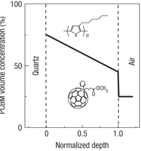
(Goffri 2006) Solvent evaporation and solubility can also generate vertical segregation as seen
in P3HT:PS blends. At room temperature the P3HT solidifies, but the PS remains in a liquid
state and can only be solidified after the removal of most of the solvent. This in effect buries
the P3HT nanofibers into a PS matrix creating preferential phase segregation. (Qiu 2009) If
one material within a blend is significantly less soluble in a common solvent with the other
component, then as the film is cast and the solvent begins to evaporate the first component of
the blend to solidify will be expelled to the film air and film substrate interfaces, Figure D.
9
Figure D. Segregation created through solubility differences between materials during spin casting. (Smith 2010)
Crystallization order and kinetics due to solvent evaporation is also a key contributor
to lateral segregation within a film. Initially, when a film is cast preferential wetting of the
interfaces occurs. However, as the solvent begins to evaporate the film thickness begins to
decrease until it reaches a critical juncture at which time the interface between the polymers
become unstable resulting in lateral segregation within the film. (Heriot 2005)
Figure E. Lateral segregation created from solvent evaporation during spin casting. (Heriot 2005)
A similar explanation for lateral segregation formed during spin casting of a binary
system is the incompatibility of polymers in a common solvent and mass transport limitations
of a material. The centripetal forces parallel to the substrate surface during spin coating
encourages this segregation as the materials within a blend solidify and move away from the
10
film solidifies first while the other is still dissolved in the solvent the particulates from that
material will be expelled away from the center of the substrate while the other material will
solidify somewhat uniformly creating lateral segregation. In the work presented here both
lateral and vertical segregation occur within the film. The high performance donor acceptor
polymer PCDTPT is much less soluble in the solvent than P3HT. It is therefore believed that
it solidifies first during spin casting causing it to be laterally segregated as well as expelled
towards the interfaces. This conclusion is coupled with the experimental contact angle results
that indicate PCDTPT will preferentially wet the substrate. Vertical segregation of PCDTPT
to the substrate interface is electrically beneficial for this blend system as the charge transport
characteristics resemble PCDTPT when the film is placed in an OTFT architecture. However,
as the film becomes increasingly thin spinodal decomposition occurs and the interface of the
bilayer becomes unstable. This results in intermixing of the two components at the interfaces
which significantly improves the ductility of the film. Thus, by blending these two components
the goal of retaining charge transport in a film is achieved while the ductility is significantly
improved.
1.2Device Physics of OFETs 1.2.1 Organic Polymers
An organic polymer is nothing more than a chain of Carbon bonds composed of repeating
structural units called monomers. In nature, this is seen in the repeating units of amino acids,
11
The chain of molecules forming these polymers are held together with covalent bonds which
holds the atoms and groups together to form a relatively fixed arrangement. It is therefore
important to pause and take some time note the importance of Carbon in all of this. Carbons
intrinsic properties are what allow for both the natural occurrence and synthetic processing of
these organic polymers. First, Carbon is relatively small in size with an atomic radii of
approximately 70 pm reducing the probability of steric hindrance. This allows Carbon to form
a substantially diverse group of chemical compounds. Steric hindrance occurs when the spatial
structure of a molecule either completely prevents or retards intermolecular or intramolecular
interactions by lowering the rate of chemical reaction compared to reactions observed in
smaller structures of related molecules. Carbon also has a modest electronegativity of 2.5 on
the Pauling scale which enables it to more readily form covalent bonds with a large number of
materials. In a covalent bond electrons are shared to create a stable balance of the repulsive
and attractive forces associated with each atom. This bonding can include π bonding and the
sharing of electrons that are not associated with a single atom, delocalized electrons, the
importance of which will be discussed later. This large versatility gives Carbon the ability to
form long polymer chains which can greatly impact the physical properties of the polymer.
The longer the chain length the stiffer the material, as described earlier in polymer blending
with the addition of aromatic rings to the polymer backbone. Finally, Carbon has the ability
to bond in several different forms including single, double and triple bonds which is important
because it permits the atomic orbitals the capacity to hybridize into three different geometries
12
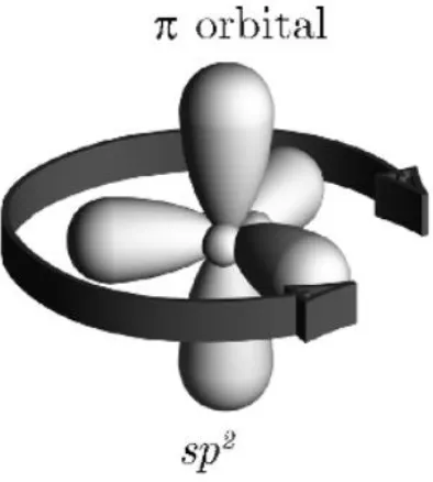
Figure F. Depiction of the sp2 hybridization with its π orbital. (Kymissis 2009)
Of particular interest is the sp2 hybridization as materials with neighboring Carbon atoms that
are sp2 hybridized can form delocalized clouds of pi electrons. These electrons therefore do
not belong to any specific atom, but instead are shared by a group of atoms. This delocalization
of the pi electrons is also what designates a material as conjugated. (Kymissis 2009) The
delocalization also creates an energy well modeled by the quantum mechanical particle in a
box. This model describes an oscillating particle contained within a box in terms of a
wavefunction which is determined by solving Schrodinger’s equation. The frequency of these
oscillations by the particle is given by a wavenumber which is directly related to the energy of
the particle. In the scenario presented here, the electrons are the particle and the molecule is
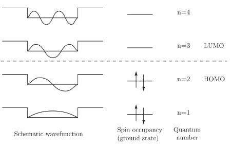
the box. This in turn gives the system discrete and differentiable energy levels that can be
represented by molecular orbitals. For semiconductors this model has two orbitals of interest,
the highest occupied molecular orbital (HOMO) and the lowest unoccupied molecular orbital
13
solid state physics to call the HOMO level the valence band and the LUMO the conduction
band.
Figure G. Diagram of HOMO and LUMO levels. (Kymissis 2006)
Should an electron within the HOMO level receive enough energy to generate an excited state
by “jumping” the bandgap an electron-hole pair is formed. This can only occur when the
oscillation of the delocalized electron is at the resonant frequency. Where the resonant
frequency is defined as the preferential frequency with which a system can oscillate such that
the response amplitude is at a relative maximum. For conjugated systems the energy required
to raise a pi electron to an excited state is relatively small and typically occurs in the visible
spectrum. (Hecht 2002) When this excitation occurs the electron now in the LUMO level and
the hole in the HOMO level are free to move creating a current. In polymers the free moving
charges achieve optimum travel through intrachain movement along the backbone of the
polymer. (Lan 2009) Being able to successfully align the polymer backbone would therefore
be greatly beneficial to advancing the propagation of the charges through the film. However,
these charges also need to travel between chains when discontinuities are encountered.
14
regions of the polymer to the electrodes where they can be harvested which is the fundamental
goal of electronic devices such as OFETs and OPVs.
1.2.2 Transistors
Transistors are the backbone for modern circuitry as they can act in two distinct
manners, as either an amplifier or a switch. As an amplifier the current flowing from the source
to the drain is equal to the control current multiplied by some factor. This mode is common in
bipolar transistors. As a switch the transistor operates in two regimes the saturation and
cut-off. When in the saturation regime the transistor is “on” while in the cut-off the transistor is
“off”. This action is what deems it as a switch and is common place in field effect transistors
which is the focus of this work moving forward. Field effect transistors utilize the physical
phenomena known in physics as the field effect. It allows an input voltage to control the flow
of the current through the device. The term field effect describes how the conductivity of a
semiconductor can change based on an applied external electric field. The transistor controls
the flow of electrons or holes, depending on the type of material p or n, traveling between the
15
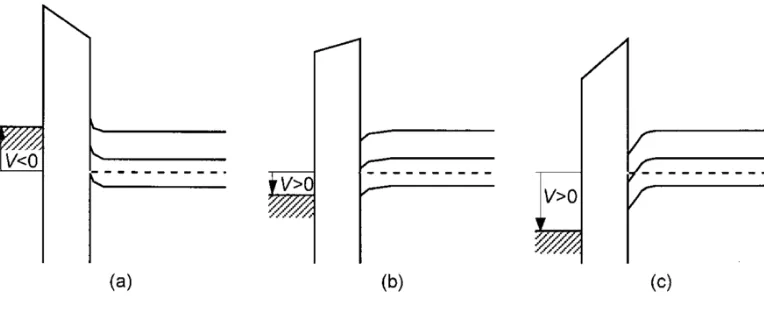
Figure H. a) Band diagram in the accumulation regime. b) Band diagram in the depletion regime. c) Band diagram in the inversion regime. (Horowtiz 1998)
In the accumulation regime a negative voltage is applied and the bands bend upwards
with the top of the valence band approaching the Fermi level. Where the Fermi level describes
the maximum energy state in which no electrons have enough energy to surpass. When a
positive voltage is applied to the system the bands bend the opposite way, in the depletion
regime. Finally, the inversion regime occurs if a significantly large positive voltage is applied
than the bands bend even further downward such that the intrinsic level surpasses the Fermi
level. Where the intrinsic level is a Fermi level located close to the center of the energy
bandgap. (Horowitz 1998) This electric field is applied to the gate which is one of three
terminals that define the transistor architecture. In this work the gate will be Si with an oxide
layer acting as the dielectric. Dielectrics are materials with very low electrical conductance
allowing an electric field to be sustained with low current leakage. The other two terminals
are the drain and source electrodes which are composed of a conductive metal. For p-type
polymers the electrodes are usually high work function methods (e.g. gold, silver or platinum)
and in this work the electrodes will be gold. Along with these terminals there is an exceedingly
thin semiconducting layer which in this work will be the polymer blend in question. There are
16
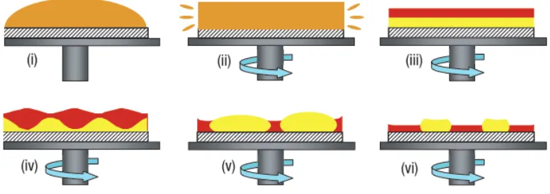
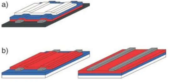
semiconductor film is placed onto the substrate surface on top of the source and drain
electrodes, and the gate electrode is evaporated on top of the film. In a bottom gate transistor
the electrodes are either evaporated onto the substrate and the semiconductor film is applied
on top in a bottom contact architecture, or the semiconductor is placed on the substrate and the
electrodes are evaporated on top of the film in a top contact architecture, see Figure I. In this
work bottom gate, bottom contact transistors were utilized.
Figure I. Architecture of field-effect transistors. a) top-gate configuration. b) bottom gate configuration, left is bottom contact, right is top contact. Black - substrate, gray - electrodes,
red – semiconductor, blue – insulator, white – gate electrode. (Allard 2008)
To operate the device a voltage is applied to the gate which is used to control the
amount of current that flows between the two electrodes through the semiconducting polymer.
This work utilized a p-type OFET so a negative voltage had to be applied which in turn causes
a flow of holes to travel from the drain to the source. For n-type OFETs a positive voltage is
applied and electrons flow from the source to the drain. To measure device performance two
values are typically assessed, the charge mobility and the on/off ratio of the drain current. As
previously stated, the charge mobility characterizes how quickly either an electron or hole can
move through the semiconductor under the applied electric field. The on/off current ratio
17
saturation current to the leakage current. The saturation current is the maximum current
achieved in a transistor under certain parameters, as it can be affected by factors such as
temperature. Obviously, it is desired that the off state be as close to zero as possible in order
for the on/off ratio be as high as possible. Physically, current leakage results in a gradual loss
of energy and in semiconductors, leakage increases power consumption and can lead to device
failure. Currently, on/off ratios have been reported as high as 108-1010.
2. MULTI-COMPONENT POLYMER FILMS TO SIGNIFICANTLY INCREASE DUCTILITY OF HIGH PERFORMANCE POLYMER SEMICONDUCTORS 2.1. Introduction and OTFT performance
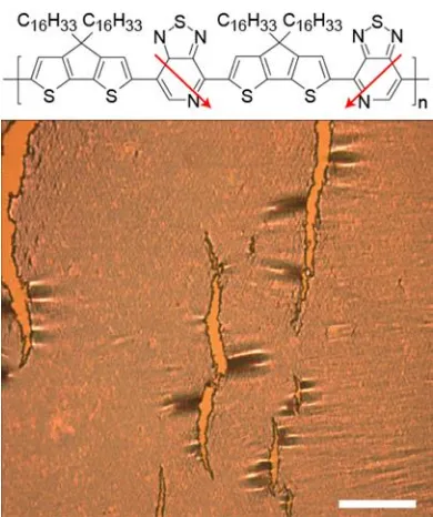
In this work, we consider the high performance donor-acceptor polymer
poly[4-(4,4-
dihexadecyl-4H-cyclopenta[1,2-b:5,4-b’]dithiophen-2-yl)-alt-[1,2,5]thiadiazolo[3,4-c]pyridine] (PCDTPT) (Figure 1). The crack onset strain of PCDTPT occurs at 4 % strain as
determined by optical microscopy. A neat PCDTPT film strained by 10 % is featured in Figure
18
Figure 1. Optical microscope image of cracked PCDTPT at 10% strain. The scale bar is 40 μm. Top, molecular structure of PCDTPT
To improve film ductility we consider blending this polymer with regioregular
poly(3-hexylthiophene) (P3HT). This approach significantly increases film ductility while the charge
transport characteristics in an OTFT configuration are largely maintained. The use of the
polymer semiconductor P3HT as the secondary material is a departure from previous studies
where the secondary material has typically been an inert or insulating polymer. P3HT was
chosen as the secondary polymer for several reasons. The high molecular weight P3HT used
in this study is known to be ductile at room temperature with a glass transition temperature
below room temperature. (Ngo 2012, Zhao 1995) P3HT is semicrystalline with strong
aggregation characteristics that will promote segregation of the polymers. P3HT is a well
characterized system allowing variations in morphology to be probed optically and with
19
the absorption spectrum of P3HT does not significantly overlap with the absorption spectrum
of PCDTPT, allowing the components to be characterized by UV-visible optical spectroscopy.
Blend films were cast from solutions composed of 1:0, 1:1, and 1:4 weight ratio of
PCDTPT:P3HT dissolved in a 1:1 volume ratio of 1,2-dichlorobenzene:chloroform. The
solutions were spun cast at room temperature onto octyltrichlorosilane (OTS) treated Si
substrates. Charge transport characteristics were measured in a bottom gate bottom contact
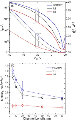
OTFT configuration with a focus on saturated field effect mobility. The transfer and output
characteristics of 5 m devices are given in Figure 2, the channel length dependence of the
20
Figure 2. (a) OTFT transfer curves for 5 m devices for neat PCDTPT, 1:1 PCDTPT:P3HT, and 1:4 PCDTPT:P3HT blend films. (b) Chanel length behavior of the saturated field effect
mobility for these films.
We find that the neat PCDTPT film has the highest saturated field-effect mobility and that
the 1:1 blend film follows closely behind with similar channel length behavior. In contrast,
when analyzing the 1:4 film, there is a slight drop in mobility and a flatter channel length
dependence, suggesting increased contact resistance. (Torsi 1995, Tukagoshi 2007) The high
21
charge transport within this blend system. While there is a drop in mobility for the 1:4 film,
PCDTPT is still believed to be the primary charge carrier material given that historically P3HT
has been shown to have an order of magnitude lower mobility. (Bao 1996, Sirringhaus 1999)
The charge transport characteristics suggest that there is vertical segregation of the materials
within the film with the PCDTPT preferentially segregating to the bottom film substrate
interface. In the following we first discuss the film morphology followed by the impact of
blending PCDTPT with P3HT on film ductility.
2.2. Film morphology
We begin the morphological characterization by first investigating the segregation
behavior of the polymers within the blend. Segregation in polymer blends commonly occurs
due to the low entropy of mixing. (Arias 2006) Entropy is a measure of the irreversibility of a
process, the higher the entropy the greater the irreversibility indicating a larger intermixing of
the two components within the blend system. Therefore, low entropy mixing will have low
process irreversibility meaning there will be greater segregation within the film. This
segregation can be both lateral and vertical within a film. (Arias 2006) Several factors can
contribute to the vertical segregation within the film including the interaction energy between
the film/substrate and film/air interfaces, (Arias 2006, Campoy-Quiles 2008, Germack 2010,
Iyengar 1996, Shin 2013) crystallization order of the components, (Goffri 2006) and solubility
differences of the materials in the solution. (Heriot 2005, Qiu 2009) In spun cast films, a lateral
segregation can also develop due to polymer interface instabilities during solidification.
22
Lateral segregation is first considered with inspection by optical microscopy and atomic
force microscopy (AFM), with characteristic images shown in Figure 3 and Figure 4, respectively.
Figure 3. Optical microscope image of unstrained (0%) and 75% strained blend films. a) 1:1 PCDTPT:P3HT unstrained film. b) 1:4 PCDTPT:P3HT unstrained film. c) 1:1
PCDTPT:P3HT 75% strained film. d) 1:4 PCDTPT:P3HT 75% strained film. The scale bar in the image is 40 m. (e) Higher magnification microscope image of laterally segregation in
23
Figure 4. Atomic force microscope images of the spun cast (a) 1:1 and (b) 1:4 ratio PCDTPT:P3HT blend films. Images of 75% strained (c) 1:1 and (d) 1:4 ratio PCDTPT:P3HT
blend films. The applied strain direction is given in the bottom left corner of the strained films. All images are 10 m by 10 m.
We see that the 1:1 film has nanoscale nodules that can be attributed to lateral segregation
of PCDTPT within the film. This is supported in part by the distinct color of the nodules
observed in the microscope image. In the 1:4 blend, the film appears to be continuous
suggesting that there is no significant lateral segregation of the polymers. To determine the
vertical segregation characteristics, the blend films were measured with Time-of-Flight
Secondary Ion Mass Spectrometry (TOF-SIMS). TOF-SIMS profiles for the 1:1 and 1:4 films
24
Figure 5. (a) Schematic of the segregation character of the 1:1 and 1:4 blend films. (b,c) TOF-SIMS results for vertical segregation of the (b) 1:1 and (c) 1:4 blend film on a Si
substrate with native oxide layer. The CN- ion is unique to the PCDTPT polymer.
In the polymers under consideration, the nitrogen within the PCDTPT provides a unique
marker for depth profiling through the CN- ion. Also shown in the TOF-SIMS depth profile is
25
segregation of the PCDTPT is clearly visible, and the blend films can be roughly divided into
3 regions. The bottom of the film is PCDTPT rich, the middle of the film has a significantly
reduced PCDTPT signature, and the top of the film we find that the PCDTPT begins to increase
again in concentration, as illustrated in Figure 5(a). The relative fraction of the PCDTPT in
the center of the film is greater in the 1:1 film compared to the 1:4 film, likely due in part to
the lateral segregation of the PCDTPT resulting in pure aggregates that form through the film
thickness. In addition, as the ratio of PCDTPT in the blend drops, the PCDTPT rich bottom
layer becomes thinner. While clear vertical segregation is measured with TOF-SIMS, the
purity of the bottom PCDTPT rich region is unknown. To estimate the purity near the surface
of the film, X-ray photoelectron spectroscopy (XPS) measurements are made on neat P3HT
and PCTPT films as well as 1:4 blend films, with data provided in Figure 6 These XPS measurements probe to roughly 10 nm of depth into the film. Results show that the bottom
surface of the blend film has signatures associated with both P3HT and PCDTPT. Thus, while
there is segregation of the PCDTPT to the bottom surface of the film, a fraction of P3HT
26
Figure 6. XPS data of PCDTPT, P3HT, and 1:4 PCDTPT:P3HT films. a) is a survey, b) is C 1s and c) is S 2p.
The vertical segregation observed in the films is attributed to a complex interplay of surface
energies and preferential solubility of the polymers. The surface interactions are first
considered by measuring the contact angle of saturated PCDTPT and P3HT solutions in
Dichlorobenzene on OTS-treated Si. The contact angles were determined to be 42o for
PCDTPT and 52o for P3HT. This suggests that PCDTPT will preferentially wet the substrate
surface. (Salleo 2007) In addition to surface energy, preferential solubility of the polymers
can also drive vertical segregation. During spin coating, solvent evaporation from the top of
the film is faster then solvent diffusion through the film. (Heriot 2005) Thus, the polymer with
lower solubility will be driven towards the substrate during spin casting. In this case, PCDTPT
is not as soluble as P3HT in the co-solvent mixture, and is thus driven toward the bottom
surface. The surpersaturated solution near the bottom surface may then undergo surface
27
Salleo 2007) However, the spin cast process results in fast solidification resulting in kinetically
limited polymer organization and some polymer intermixing throughout the film. This limited
segregation appears to impact the solution with lower PCDTPT content resulting in the lower
performance in the 1:4 blend film as compared to the 1:1 film. It should be noted that the
processing approach used here is a fast cast method processed at room temperature. This
approach simplifies the casting procedure considerably compared to previous methods that
require elevated temperature casting with fine control of solidification order and rate. (Goffri
2006) Nor does the method use a marginal solvent approach to promote polymer segregation
that requires careful solution design. (Qiu 2009, Sparrow 2010)
The segregation and aggregation disposition of the blend films are further characterized
with visible spectroscopy and grazing incidence X-ray diffraction (GIXD). The
UV-visible absorbance of the films is given in Figure 7.
Figure 7. UV-visible analysis of PCDTPT:P3HT films under varying levels of strain. a) 1:1 PCDTPT:P3HT film with light polarized parallel to the direction of strain. b) 1:4
PCDTPT:P3HT film with light polarized parallel to the direction of strain.
Clear absorption features associated with the P3HT and PCDTPT are present and their
relative contribution associated with the concentration is apparent. The vibronic features
28
in the cast film. Neat PCDTPT film absorption is roughly from 700 nm to 1100 nm and is
rather featureless, and this absorption characteristic remains similar in the blend films at this
range. Interestingly, PCDTPT has a secondary peak at roughly 475 nm which is seen as a
distinct shoulder in the 1:1 blend film system. Grazing incidence X-ray diffraction of the neat
P3HT, neat PCDTPT and the 1:4 blend films are given in Figure 8.
Figure 8. GIXD images of neat film components and 1:4 blend film. Top is neat P3HT film, Middle is PCDTPT film and bottom is 1:4 PCDTPT:P3HT blend film.
In the neat films, it is clear that both films are semicrystalline with characteristically
29
films, characteristic packing features from the P3HT and PCDTPT components are present.
The diffraction character of the PCDTPT in the blend films is difficult to observe due to the
relatively low concentration of PCDTPT and the overlapping diffraction peaks of P3HT and
PCDTPT. The alkyl stacking distance in PCDTPT is larger than P3HT and the -stacking
distance is shorter, such that the diffraction peaks are separated in reciprocal space. The unique
peaks from each polymer crystal are observable in the blend film. Thus, the P3HT and
PCDTPT continue to form neat crystals within the film and no co-crystal formation or chemical
interaction is apparent. Also, the higher order (h00) peaks and the (010) peak observed in the
neat PCDTPT films become significantly weaker in the blend film. This is due in part to
obfuscation of the diffraction due to the large P3HT diffraction cross sectional area, but is also
likely a result of slightly increased disorder of the PCDTPT in the blend film.
2.3. Film ductility
Thus far, the films are shown to have clear aggregation of each of the polymer components
and vertical segregation of the PCDTPT towards the bottom of the device allowing for OTFTs
with performance similar to neat PCDTPT films. A primary motivation of this paper is to
explore the impact blending a film has on the mechanical behavior with particular focus on the
film ductility. To estimate changes in film ductility, we measure the onset of fracture in the
film using optical microscopy and atomic force microscopy. We further verify the fracture
nature by measuring charge transport of the strained films in an OTFT configuration.
The crack onset strain is first investigated by transfer printing the films from the initial cast
substrate onto a PDMS elastomer host, following a procedure previously described. (O’Connor
2011) The films are then strained while on the host elastomer and visually inspected by optical
30
fracture cannot be observed, with characteristics images shown in Figure 3. In the 1:1 film, the lateral segregation features may obscure the presence of fracture. A more detailed
inspection of highly strained films is performed by AFM, with images shown in Figure 4. Here, films are strained while on a PDMS elastomer and then transferred onto an OTS treated
Silicon surface. The 1:4 film appears continuous up to 75 % strain. However, 1:1 films at 50
% strain or higher show tearing features developing near the PCDTPT aggregates. Fracture is
not observed in the regions absent of these PCDTPT nodules, suggesting that this region has
increased ductility. These tearing features appear to start between 25% and 50 % strain, where
tearing can also be observed as shown in Figure 9.
Figure 9. AFM images of strained PCDTPT:P3HT films. a) 1:1 PCDTPT:P3HT film under 25% strain. b) 1:1 PCDTPT:P3HT film under 50% strain. Both images are 5 μm sized scans,
the scale bar for a) is 100 μm and for b) is 150 μm. Direction of strain is indicated by the arrow in the lower left corner of both images.
The onset of fracture in this film remains significantly larger than the neat PCDTPT films,
which cracks at strains of approximately 4 %. It is important to note that even at strains up to
75%, all fracture is isolated to the interface of the PCDTPT aggregates and no tearing is
observed within the vertically segregated portion of the film. Thus, both the vertical segregated
31
observed in the 1:4 blend films results in highly ductile films. To gain insight into the plastic
deformation occurring in the films, absorbance anisotropy is measured in the films with applied
strain, with results shown in Figure 10.
Figure 10. Absorbance anisotropy of the a) 1:1 PCDTPT:P3HT and b) 1:4 PCDTPT:P3HT blend systems. Solid lines indicate absorbance parallel to strain while dashed lines indicate
absorbance perpendicular to strain.
We find that as the film is strained an absorption anisotropy develops over the wavelength
range corresponding to both P3HT and PCDTPT absorption. Given that the optical transition
dipole moment in conjugated polymers is typically along the polymer backbone, the measured
absorbance anisotropy indicates that both polymers are aligning in the direction of strain.
(Clark 2007, Gargi 2013, O’Connor 2011)To quantify the anisotropy, we plot the dichroic ratio
(R) of the blend films with strain, where R = A׀׀/A⊥, and A is the absorbance of the film with
32
Figure 11. Dichroic ratio of the 1:1 and 1:4 PCDTPT:P3HT films with strain evaluated at 550 and 900 nm
R is taken at the wavelengths of 550 nm and 900 nm representing the peak absorption
associated with P3HT and PCDTPT, respectively. (O’Connor 2011, Tseng 2012, Ying 2011)
In the strained 1:4 film, R at 550 nm and 900 nm are similar at 50 % applied strain, but deviates
slightly at 75 % where the P3HT component of the film (550 nm) is shown to have a larger R.
In the 1:1 blend film, R is larger at 550 nm (P3HT component) than 900 nm (PCDTPT
component) at both 50 % and 75 % strain. These results show that both polymers are
reorienting with plastic deformation. The larger divergence observed in the 1:1 film is likely
due to the laterally segregated PCDTPT aggregates that do not plastically deform and thus
have isotropic absorbance for normal incidence light. The aggregates may also act as pinning
sites where large amounts of stress accumulate as a result of the geometric irregularity of the
PCDTPT aggregates. These stresses act on the P3HT forcing it to undergo larger reorientation
33
Finally, strained films are printed onto OTFT test beds and thermally annealed to improve
local order. Charge mobility is measured parallel to the direction of strain. However, it should
be noted that cast films can be thermally annealed at 200°C and maintain ductility similar to
the as-cast films While charge transport is able to overcome some holes in a film, it is expected
that cracking will result in a decrease in the measured field effect mobility. (Cairns 1999,
O’Connor 2010) The field effect mobility with applied strain, for 5 μm channel length devices,
is given in Figure 12.
Figure 12. Saturated field effect mobility in the blend films with applied strained for charge transport parallel to the strain direction. The unstrained neat PCDTPT mobility is shown as a
dotted line with uncertainty in gray, and is shown to compare to the strained films. The channel length of the devices was 5 m.
We see that the mobility increases with strain for both the 1:1 and 1:4 blend films with
maximum achieved mobility values of 1.20 cm2V-1s-1 and 0.74 cm2V-1s-1, respectively. These
mobilities are comparable to values achieved with neat PCDTPT films. (Tseng 2012) This
34
2011) associated with alignment of the polymer backbone in the direction of strain. (Lan 2009,
O’Connor 2012) Here, we see that the relative increase in mobility of the 1:4 strained film is
larger than the 1:1 film. This may be due in part to lowered contact resistance with strain in
the 1:4 films. In addition to the increase in mobility with strain, the 1:1 films appear to dampen
at large strains. This is likely due to the tearing in the film. The channel length behavior in the
strained films is also different between the 1:1 and 1:4 films, shown in Figure 13.
Figure 13. Channel length dependence measured parallel to strain (a) 1:1 PCDTPT:P3HT (b) 1:4 PCDTPT:P3HT
The relative mobility increase in the 1:4 strained films is similar for short and long channel
lengths. In the 1:1 films, the long channel length mobility does not improve with strain. This
lack of improvement at large strains may be associated with nanoscale tearing of the primary
transport materials (PCDTPT). This is consistent with previous work on charge transport in
oriented pBTTT films, where film discontinuity limits long channel length mobility
enhancement. (Hamadini 2007) We find that charge transport is able to overcome some film
35
1:4 films, a clear difference in behavior is observed associated with a discontinuous 1:1 film
that develops at large strains.
3. SUMMARY
3.1 Conclusions
The work presented here has implications for future work and significance within the
field of semiconductor blends and organic thin film transistors. The addition of a secondary
polymer to the brittle donor-acceptor semiconductor PCDTPT significantly increases the film
ductility, for both blend film ratios levels of strain up to 75% were achieved which is
significantly greater than neat PCDTPT films, while charge transport characteristics are largely
maintained, with mobility values being achieved as high as 1.20 cm2V-1s-1. This ability to
maintain good charge transport behavior is directly attributed to the vertical segregation of the
high performance PCDTPT to the substrate interface as seen in the TOF-SIMS measurement.
Vertical segregation of the PCDTPT towards the gate dielectric interface is largely beneficial
for charge transport as it has been previously shown that charge transport in transistors takes
place within roughly 10 nm of the substrate surface. In this system PCDTPT is well within
this region. Mechanically, the large increase in film ductility is attributed to the bulk of the
film being composed primarily of the ductile P3HT with the interfaces contain an
inter-dispersed layer of PCDTPT and P3HT as confirmed with XPS measurements. Yet, it may be
possible that the surface of the film has increased ductility due to surface confinement within
the thin film architecture. (Stafford 2006, Yoshimoto 2005) This potentially could increase
36
at the center of the film would remain primarily highly ductile. These results are significant
as until now there has been very limited research in non-block copolymers that consider how
the vertical segregation within a film effect overall film ductility. Importantly, the improved
mechanical capability of the blend system does not degrade charge transport characteristics
within the film, but instead enables strain oriented films. Mobility in the direction of applied
strain increases compared to the unstrained film. The resulting anisotropy is a result of
increased polymer backbone alignment in the direction of applied strain, where charge
transport is the most efficient. A significant channel length dependence phenomena arises
within the 1:1 PCDTPT:P3HT film but is significantly less dominant in the 1:4 PCDTPT:P3HT
film. This difference in channel length behavior between the two blend systems can be directly
attributed to the nanoscale fractures around the PCDTPT aggregates. As charge transport
occurs within the film it must hop between chains and disordered regions. For short channel
lengths the amount of hops that the charge must undertake is minimal. As the channel length
increases the amount of chains, discontinuities from fractures and grain boundary disorder the
charge must overcome increases. Thus, it is inevitable that some charges will be lost and
charge transport for these longer channel length devices will be significantly less efficient.
Another significant feature of this vertical segregation is the processing conditions
under which it is achieved. To attain this preferential vertical segregation no special processing
techniques were needed as the film can be spun cast onto OTS treated Silicon for fast drying
at room temperature. However, it is important to note that the PCDTPT is less soluble in the
solvent pair than P3HT such that it solidifies first and is expelled to the interfaces. This is
directly contrasting with previous work where slow drying times were required and control of
37
PCDTPT:P3HT blend retains the good mechanical properties of the P3HT and the electrical
properties of the PCDTPT highlighting the material opportunities for high performance
polymer semiconductor transistors that have been electrically and mechanically optimized.
3.2 Future Work
The work that has been completed to this point has raised several different points of
interest on directions to take this research moving forward. Optimizing the PCDTPT:P3HT
blend such that maximum electrical and mechanical properties are achieved is an interesting
project moving forward. In organic photovoltaic devices the structure of the bulk
heterojunction (BHJ) plays an integral part in the device performance, particularly when
utilizing donor-acceptor polymer blends such as P3HT and PCBM. The morphology typically
contains phase segregated domains of the materials that are utilized within the blend system
for the BHJ. This allows for networks to be formed that promotes dissociation and charge
transport while hopefully limiting charge recombination mechanisms. In this work, the blend
system exhibits both lateral and vertical phase segregation of the donor-acceptor PCDTPT and
donor P3HT that makes it a potentially intriguing option for the BHJ of a ternary organic
photovoltaic device (OPV). The vertical segregation also presents an interesting question
about the interfacial adhesion properties of the blend system. Particularly, the fact that when
the P3HT is strained the crystal orientation changes from an edge on to face on orientation.
This raises the question, if the orientation is adjusted such that there is greater face on
orientation how will this effect the adhesion properties? It is my assumption that by rotating
P3HT into a face on orientation the adhesion energy will increase as the aromatic ring of the
backbone is exposed. By varying the levels of strain and resulting face on orientation the
38
DTS Delaminator system. Currently, only preliminary experiments have been completed using
P3HT:PCBM blends without a preference of orientation. Due to the size of the specimens the
solution must be flow coated onto the substrate. While it has been shown in previous work
that flow coating can orient the polymer, developing a method for accurately achieving this
will need to be accomplished to move forward with this project. Another potential area of
interest is the completely flexible transistor which has been made before with some success.
(Briseno 2006, Fukuda 2014) While the most electrically capable blend system used here, 1:1
P3HT:PCDTPT, begins tearing between 25% and 50% strain, charge mobility is able to
overcome these discontinuities. By placing this film onto a flexible substrate the transistor
could potentially be strained to similar levels and achieve relatively good charge transport. An
interesting aspect of this would be to see the charge transport fatigue and device hysteresis
after periods of induced and released strain. Several questions arise from this thought. Would
the film recover such that the nanoscale tearing around the PCDTPT aggregates would no
longer be evident when the strain is released? Would charge transport return to its pre-strained
levels? Finally, if the device is strained repeatedly at the same level how would the nanoscale
39 4. REFERENCES
Allard, S., M. Forster, B. Souharce, H. Thiem, and U. Scherf (2008). “Organic
Semiconductors for Solution-Processable Field-Effect Transistors (OFETs),” Angew. Chem. Int. 47, 4070-4098.
Arias, C (2006). “Vertically Segregated Polymer Blends: Their Use in Organic Electronics,” J. Macr. Sci. Pt. C: Poly. Rev. 46,103-125.
Berggren, M., O. Ingana, J. Gustafsson, G. Rasmusson, M. Andersson, T. Hjertberg and O. Wennerstrom (1994). “Light Emitting Diodes with Variable Colours from Polymer Blends,” Lett. To Nat. 372, 444-446.
Biniek, L., B. Schroeder, C. Nielson and I. McCulloch (2010). “Recent Advances in High Mobility Donor-Acceptor Semiconducting Polymers,” J. Mater. Chem. 22, 14803-14813.
Bjortstrom, C., S. Nilsson, A. Bernasik, A. Budkowski, M. Andersson, K. Magnusson and E. Moons (2007). “Vertical Phase Separation in Spin-Coated Films of Low Bandgap Polyflourene/PCBM Blend – Effetcs of Specific Substrate Interactions,” Appl. Surface Sci. 253, 3906-3912.
Boltau, M. Walheim, S., Mylnek, J., Krausch, G. and Steiner, U. (1998). “Surface-induced Structure of Polymer Blends on Patterned Substrates,” Nature, 391, 877-879.
Brinkmann, M. and P. Rannou (2007). “Effect of Molecular Weight on the Structure and Morphology of Oriented Thin Films of Regioregular Poly(3-hexylthiophene) Grown by Directional Epitaxial Solidification,” Adv. Funct. Mater. 17, 101-108.
Brinkmann, M. and J. Wittmann (2006). “Orientation of Regioregular
Poly(3-hexylthiophene) by Directional Solidification: A Simple Method to Reveal the Semicrystalline Structure of a Conjugated Polymer,” Adv. Mater. 18, 860-863.
40
Cairns, D., R. Witte, D. Sparacin, S. Sachsman, D. Paine and G. Crawford (1999). “Strain-dependent Electrical Resistance of Tin-doped Indium Oxide on Polymer Substrates,” App. Phys. Lett. 76, 1425-1427.
Campoy-Quiles, M., T. Ferenczi, T. Agostinelli, P. Etchegoin, Y. Kim, T. Anthopoulos, P. Stavrinou, D. Bradley and J. Nelson (2008). “Morphology Evolution via Self-Organization and Lateral and Vertical Diffusion in Polymer:Fullerene Solar Cell Blends,” Nat. Mater. 7, 158-164.
Chen, X. and J. Gardella (1994). “Surface Modification of Polymers by Blending Siloxane Block Copolymers,” Macromolecules. 27, 3363-3369.
DeLongchamp, D., R. Kline, Y. Jung, D. Germack, E. Lin, A. Moad, L. Richter, M. Toney, M. Heeney and I. McCulloch (2009). “Controlling the Orientation of Terraced Nanoscale “Ribbons” of a Poly(thiophene) Semiconductor,” Nano. 3, 780-787.
Drury, C., C. Mutsaers, C. Hart, M. Matters and D. de Leeuw (1998). “Low-cost All-polymer Integrated Circuits,” App. Phys. Lett. 73, 108-110.
Ferenczi, T., C. Muller, D. Bradley, P. Smith, J. Nelson and N. Stingelin (2011). “Organic Semiconductor:Insulator Polymer Ternary Blends for Photovoltaics,” Adv. Mater. 23, 4093-4097.
Forrest, S. (2004). “The Path to Ubiquitous and Low-cost Electronic Applications on Plastic,” Nature. 428, 911-918.
Fukuda, K., Y. Takeda, M. Mizukami, D. Kumaki and S. Tokito (2014). “Fully Solution-Processed Flexible Organic Thin Film Transistor Arrays with High Mobility and Exceptional Uniformity,” Sci. Rep. 4, 4-11.
41
Germack, D., C. Chan, R. Klein, D. Fischer, D. Gundlach, M. Toney, L. Richter and D. DeLongchamp (2010). “Interfacial Segregation in Polymer/Fullerene Blend Films for Photovoltaic Devices,” Macromolecules. 43, 3828-3836.
Goffri, S., C. Muller, N. Stingelin-Stultzmann, D. Breiby, C. Radano, J. Andreasen, R. Thompson, R. Janssen, M. Nielsen, P. Smith and H. Sirringhaus (2006).
“Multicomponent Semiconducting Polymer Systems with Low Crystallization-induced Percolation Threshold,” Nat. Mater. 5, 950-956.
Goubard, F. and G. Wantz (2014). “Ternary Blends for Polymer Bulk Heterojunction Solar Cells,” Polym. Int. 63, 1362-1367.
Halls, J., C. Walsh, N. Greenham, E. Marseglia, R. Friend, S. Moratti and A. Holmes (1995). “Efficient Photodiodes from Interpenetrating Polymer Networks,” Nat. 376, 498-500.
Hamadini, B., D. Gundlach (2007). “Undoped Polythiophene Field-effect Transistors with Mobility of 1 cm2V-1s-1,” Appl. Phys. Lett. 91, 1-4.
Hamilton, R., J. Smith, S. Ogier, M. Heeney, J. Anthony, I. McCulloch, J. Veres, D. Bradley and T. Anthopoulos, (2009). “High Performance Polymer-Small Molecule Blend Organic Transistors,” Adv. Mater. 21, 1166-1171.
Hecht, E. (2002). The Propagation of Light. In Optics (4th ed., pp. 134-135). San Fransisco, CA: Pearson Education.
Heriot, S. and R. Jones (2005). “An Interfacial Instability in a Transient Wetting Layer Leads to Lateral Phase Separation in Thin Spin-cast Polymer-blend Films,” Nature Mater. 4, 782-786.
Horowitz, G (1998). “Organic Field-effect Transistors,” Adv. Mater. 10, 365-377.
42
Iyengar, D. , S. Perutz, C. Dai, C. Ober and E. Kramer (1996). “Surface Segregation Studies of Fluorine-Containing Diblock Copolymers,” Macromolecules. 29, 1229-1234.
Koezuka, H. (1987). “Field-effect Transistor with Polythiophene Thin Films,” Synthetic Metals. 18, 699-704.
Kymissis, I. (2009). "The Physics of Organic Semiconductors." Organic Field Effect Transistors: Theory, Fabrication and Characterization. New York: Springer.
Lan, Y. and C. Huang (2009). “Charge Mobility and Transport Behavior in the Ordered and Disordered States of Regioregular Poly(3-hexylthiophene),” J. Phys. Chem. B. 113, 14555-14564.
Moulton, J. and P. Smith (1991). “Gel Processing of Electrically Conductive Blens of Poly(3-octylthiophene) and Ultrahigh Molecular Weight Polyethylene,” J. Poly. Sci. Pt. B. 30, 871-878.
Ngo, T., D. Nguyen and V. Nguyen (2012). “Glass Transition of PCBM, P3HT and their Blends in Quenched State,” Adv. Nat. Sci.: Nanosci. Nantechnol. 3, 045001-045004.
O’Connor, B., E. Chan, C. Chan, B. Conrad, L. Richter, R. Kline, M. Heeney, I. McCulloch, C. Soles and D. DeLonchamp (2010). “Correlations between Mechanical and
Electrical Properties of Polythiophenes,” ACS Nano. 4, 7538-7544.
O’Connor, B., R. Kline, B. Conrad, L. Richter, D. Gundlach, M. Toney and D.
DeLongchamp (2011). “Anisotropic Structure and Charge Transport in Highly Strain-aligned Regioregular Poly(3-hexylthiophene),” Adv. Funct. Mater. 21, 3697-3705.
Paul, D. (1978). Phase Morphology. In Polymer Blends, Volume 1 (Vol. 1, pp. 11-13). New York, New York: Academic Press.
43
Salleo, A. and Arias, A.C. (2007). “Solution based self-assembly of an Array of Polymeric Thin-film Tranistors,” Adv. Mater. 19, 3540-3543.
Scaccabarozzi, A. and N. Stingelin (2014). “Semiconducting:insulating Polymer Blends for Optoelectronic Applications – a Review of Recent Advances,” J. Mater. Chem. A. 2, 10818-10824.
Shirakawa, H., E. Louis, A. MacDiarmid, C. Chiang and A. Heeger (1977). “Synthesis of Electrically Conducting Organic Polymers: Halogen Derivatives of Polyacetylene, (CH)x” J.C.S. Chem. Comm. 578-580.
Sirringhaus, H. (2014). “25th Anniversay Article: Organic Field-effect Transistors: The Path Beyond Amorphous Silicon,” Adv. Mater. 26, 1319-1335.
Sirringhaus, H., R. Wilson, R. Friend, M. Inbasekaran, W. Wu, E. Woo, M. Grell and D. Bradley (2000). “Mobility Enhancement in Conjugated Polymer Field-effect
Transistors through Chain Alignment in a Liquid-crystalline Phase,” Appl. Phys. Lett. 77, 406-408.
Smith, J., R. Hamilton, I. McCulloch, N. Stingelin-Stitzmann, M. Heeney, D. Bradley and T. Anthopoulos (2010). “Solution-processed Organic Transistors Based on
Semiconducting Blends,” J. Mater. Chem. 20, 2562-2574.
Sparrowe, D., Baklar, M. and Stingelin, N. (2010). “Low-temperature Printing of
Crystalline:Crystalline Polymer Blend Transistors,” Organic Electronics, 11, 1296-1300.
Stafford, C., B. Vogt, C. Harrison, D. Julthongpiput and R. Huang (2006). “Elastic Moduli of Ultrathin Amorphous Polymer Films,” Macromolecules. 39, 5095-5099.
Szendrei, K., D. Jarzab, Z. Chen, A. Facchetti and M. Loi (2010). “Ambipolar All-polymer Bulk Heterojunction Field-effect Transistiors,” J. Mater. Chem. 20, 1317.
44
Tang, C. and S. VanSlyke (1987). “Organic Electroluminescent Diodes,” App. Phys. Lett. 51, 913-915.
Torsi, L., A. Dodabalapur and H. Katz (1995). “An Analytical Model for Short-channel Organic Thin Film Transistors,” J. App. Phys. 78, 1088-1093.
Tukagoshi, K., F. Fujimori, T. Minari, T. Miyadera, T. Hamano and Y. Aoyagi (2007). “Supression of Short Channel Effect in Organic Thin Film Transistors,” App. Phys. Lett. 91, 113508-113508-3.
Walheim, S., M. Moltau, J. Mylnek, G. Krausch and U. Steiner (1997). “Structure Formation via Polymer Demixing in Spin Cast Films,” Macromolecules. 30, 4995-5003.
Williams, A., P. Farrar, A. Gallant, D. Atkinson and C. Groves (2014). “Characterisation of Charge Conduction Netwroks in Poly(3-hexylthiophene)/polystyrene Blends using Noise Spectroscopy,” J. Mater. Chem. C. 2, 1742-1748.
Yoshimoto, K., T. Jain, P. Nealey and J. de Pablo (2005). “Local Dynamic Mechanical Properties in Model Free-standing Polymer Thin Films,” J. Chem. Phys. 122, 144712-144712-6.
Yu, G., A. Heeger (1995). “Charge Seperation and Photovoltaic Conversion in Polymer Composites with Internal Donor/acceptor Heterojunctions,” J. App. Phys. 78, 4510-4515.
Yu, G., K. Pakbaz, A. Heeger (1994). “Semiconducting Polymer Diodes: Large Size, Low Cost Photodetectors with Excellent Visible-ultraviolet Sensitivity,” App. Phys. Lett. 64, 3422-3424.